國 立 交 通 大 學
電子物理學系
碩 士 論 文
利用多層閘極之增強型應力記憶技術製作在
利用多層閘極之增強型應力記憶技術製作在
利用多層閘極之增強型應力記憶技術製作在
利用多層閘極之增強型應力記憶技術製作在 n
nn
n 型
型
型
型
金氧半場效電晶體之研究
金氧半場效電晶體之研究
金氧半場效電晶體之研究
金氧半場效電晶體之研究
Enhancement of Stress Memorization Technique on
nMOSFETs by Multiple Strain-Gate Engineering
研 究 生 : 王智盟
指導教授 : 趙天生 博士
利用多層閘極之增強型應力記憶技術製作在
利用多層閘極之增強型應力記憶技術製作在
利用多層閘極之增強型應力記憶技術製作在
利用多層閘極之增強型應力記憶技術製作在 n
nn
n 型
型
型
型
金氧半場效電晶體之研究
金氧半場效電晶體之研究
金氧半場效電晶體之研究
金氧半場效電晶體之研究
Enhancement of Stress Memorization Technique on nMOSFETs by
Multiple Strain-Gate Engineering
研究生:王智盟 Student:Jr-Meng Wang
指導教授:趙天生博士 Advisor:Dr. Tien-Sheng Chao
國立交通大學
電子物理學系碩士班
碩士論文
A Thesis
Submitted to Department of Electrophysics
National Chiao Tung University
In Partial Fulfillment of the Requirements
for the Degree of
Master of Science
In
Electrophysics
June 2008
HsinChu, Taiwan, Republic of China
中華民國
中華民國
中華民國
利用多層閘極之增強型應力記憶技術製作在
n 型金氧半場效電晶體之研究
指導教授 : 趙天生 博士 研究生 : 王智盟
國立交通大學
電子物理學系碩士班
摘要
在本篇論文的研究中,我們利用控制電子通道中殘留應力的技術來
製作n 型金氧半場效應電晶體,電子通道中應力的主要來源是利用元
件尚未定義出閘極前覆蓋一層Si
3N
4薄膜,接著快速退火,然後去除
Si
3N
4薄膜(SPFT technique),利用Si
3N
4薄膜本身具有的高應力特性
及多晶矽內部結構改變,產生殘留的應變,進而達到改善電子遷移率
的目的。此外,我們利用非晶矽及複晶矽兩種堆疊的結構加上SPFT
技術製作元件,這種結構的優點主要是可以增加電子通道中應力的大
小,使電子遷移率的增加幅度能夠更加顯著,我們發現同時利用閘極
堆疊結構及這種方式可以有效提昇元件的電導達24%。以上所有的元
件部份,最後皆有附加一層接觸孔蝕刻停止層(CESL),使得這項技術
可以廣泛的使用在製程內而不會有應力減小的效果。我們相信利用控
制電子通道中應力的大小來改善電流驅動能力在未來CMOS 元件技術
的發展上將扮演非常重要的角色。
Enhancement of Stress Memorization Technique on nMOSFETs by
Multiple Strain-Gate Engineering
Student: Jr-Meng Wang Advisors: Dr. Tien-Sheng Chao
Department of Electrophysics
National Chaio Tung University
Abstract
An enhanced stress memorization technique (SMT) has been
demonstrated by multiple strain-gate engineering that utilizes strain
proximity free technique (SPFT) and a stacked a-Si/poly-Si gate structure.
It is found that the transconductance (G
M) of nMOFETs with SPFT
exhibits an 18% increase compared to that of counterparts. The SPFT can
prevent the limitation of stressor volume for performance improvement in
high density CMOS circuits. We also found that the optimization of
stacked a-Si/poly-Si gate structure and combine with the SPFT can
improve the G
Mfurther to 24% more than the single-poly-Si gate
誌謝
首先我要特別感謝指導教授趙天生博士的指導與教誨,受教於趙
教授這兩年期間,讓我在獨立思考及專業知識上都有所成長,期間有
好幾次遇到挫折,幸好有老師的鼓勵讓我更能勇敢面對問題,謝謝老
師對我的細心指導與鼓勵,在此致上我最高的敬意。
此外,我也非常感謝呂宗宜學長在專業知識給我的一切協助與指
導,同時也感謝陳建豪、郭伯儀、吳偉成、馬鳴汶、羅文政、楊宗諭、
高國興、邱德馨、劉美君、猴子、妍心、阿壘等學長姐在這段期間給
我的關懷與協助,在我論文及實驗上有疑惑時常常給予解惑,在此表
達我的感激。特別感謝與我一起走過這段日子的研究夥伴,宗育、冠
迪、威良、廖俊、翊鴻、榮家以及實驗室的學弟妹們,感謝他們這段
時間的陪伴與鼓勵,有了你們讓我感到實驗室時常充滿歡笑聲,使我
更有動力邁向研究的動力,別忘了以後有空時候在一起打球及唱歌。
特別感謝心颐小姐在這些年來對我的關懷與扶持,謝謝她一路
陪我走過漫長的求學生涯並陪我渡過重重難關,最後僅以此論文獻給
我敬愛的母親以及家人,感謝他們在我一度迷失人生方向時扶持我繼
續向前,支持與鼓勵我順利完成學業。
Contents
Abstract (Chinese) .………..…...i
Abstract (English) .………..…...ii
Achnowledgement.………..…...iii
Contents.……….…...iv
Figure Captions………...………..v
Chapter 1 Introduction………...1
1-1 General Background...1 1-2 Motivation...4 1-3 Thesis Organization...5Chapter 2 Device Fabrication
...
11Chapter 3 Results and Discussion
...20
3-1 Summary of stacked a-Si/poly-Si gate structure………20
3-2 Summary of strain proximity free technique (SPFT)…………35
3-3 Summary of stacked a-Si gate structure with SPFT.………….54
3-4 Hot carrier reliability………..……..61
Chapter 4 Summary and Conclusio
n...
73Figure captions
Chapter1 Introduction
Fig. 1-1 Conduction-band structure of (a) bulk Si and (b) strained-Si…...7
Fig. 1-2 Valence band of (a) bulk Si and (b) Si under biaxial tension.…..7
Fig. 1-3 Fabrication process for locally strained channel transistor….…..8
Fig. 1-4 The cross sectional SEM images and stress distributions of nFET
and pFET………..8
Fig. 1-5 (a)Schematic illustration of process flow of CMOSFET with
DCL technique. (b)Stress simulation results (vertical strain yy)
of nMOSFETs. ………..…..9
Fig. 1-6 Voids in the dense poly regions ……….10
Fig. 1-7 Sxx distribution dependence on stress liner thickness…………10
Chapter 2 Device Fabrication……….……
13
Chapter 3 Results and Discussion
Fig. 3-1 Gate structure with different condition…………...………24
Fig. 3-2 C-V characteristics for different thickness of a-Si layer…...…..25
Fig. 3-3 I
d-V
gcharacteristics for different thickness of a-Si layer…...….26
Fig. 3-4 I
d-V
gcharacteristics for different thickness of a-Si layer.…..….27
Fig. 3-6 Threshold voltage for different thickness of a-Si layer……..…29
Fig. 3-7 DIBL for a-Si layer with different channel length………...30
Fig. 3-8 Transconductance for different thickness of a-Si layer……...31
Fig. 3-9 Transconductance increase versus channel length with different
thickness of a-Si layer………..…..…32
Fig. 3-10 I
d-V
dcharacteristics for different thickness of a-Si layer…...33
Fig. 3-11 Saturation current increase versus channel length with different
thickness of a-Si layer………...34
Fig. 3-12 Poly gate with SPFT and PAI_SPFT technique………...39
Fig. 3-13 C-V characteristics for SPFT and PAI_SPFT technique..…....40
Fig. 3-14 I
d-V
gcharacteristics for SPFT and PAI_SPFT technique…...41
Fig. 3-15 I
d-V
gcharacteristics for SPFT and PAI_SPFT technique…...42
Fig. 3-16 Threshold voltage for SPFT and PAI_SPFT technique……....43
Fig. 3-17 Threshold voltage for SPFT and PAI_SPFT technique……....44
Fig. 3-18 DIBL for SPFT and PAI_SPFT technique……….…...45
Fig. 3-19 Transconductance for SPFT and PAI_SPFT technique……....46
Fig. 3-20 Stress–strain curve showing the elastic and plastic regimes….47
Fig. 3-21 AFM image for Poly 2000 and Poly 2000_SPFT samples.…..48
Fig. 3-22 SEM image for Poly 2000 and Poly 2000_SPFT samples…...49
Fig. 3-23 Transconductance increase versus channel length with SPFT and
Fig. 3-24 I
d-V
dcharacteristics for SPFT and PAI_SPFT technique……52
Fig. 3-25 Saturation current increase versus channel length with SPFT and
PAI_SPFT technique………...53
Fig. 3-26 Id-Vg and transconductance characteristics with SPFT and
a-Si-700/poly1300_SPFT gate structure……….56
Fig. 3-27 Threshold voltage for SPFT and a-Si-700/poly1300_SPFT gate
structure ……….57
Fig. 3-28 Transconductance increase versus channel length with SPFT
and a-Si-700/poly1300_SPFT gate structure………...58
Fig. 3-29 I
d-V
dcharacteristics for SPFT and a-Si-700/poly1300_SPFT
techniques………59
Fig. 3-30 Saturation current increase versus channel length with SPFT
and a-Si-700/poly1300_SPFT gate structure………..60
Fig. 3-31 Schematic showing electron-hole pairs generation by impact
ionization due to hot electrons……….63
Fig. 3-32 Substrate current versus gate voltage with the three splits in
different channel lengths of 0.4, 0.7, 1.0 µm………...64
Fig. 3-33 Substrate current versus gate voltage with SPFT and
a-Si-700/poly1300_SPFT splits in different channel lengths of
0.4, 0.7, 1.0 µm………65
Fig. 3-34 Hot carrier stress for the three splits at Vds = 3.5 V & Vg =
I
sub_max……….66
Fig. 3-36 Subthreshold and transconductance characteristics for the SPFT
and PAI_SPFT samples before and after stress 5000 seconds.67
Fig. 3-36 Channel hot carrier characteristics for SPFT and PAI_SPFT
samples………68
Fig. 3-37 Channel hot carrier characteristics for SPFT and PAI_SPFT
samples………69
Fig. 3-38 Before and after hot carrier stress 5000 seconds for the three
splits at Vds = 3.5v & Vg = I
sub_max………70
Fig. 3-39 Channel hot carrier characteristics for SPFT and
a-Si-700/poly1300_SPFT samples………..71
Fig. 3-40 Channel hot carrier characteristics for SPFT and
Chapter 1
Introduction
1-1 General Background
In order to realize higher speed, lower power and higher packing density metal
oxide semiconductor field effect transistor (MOSFET) integrated circuit, the
semiconductor device manufacturing process technique has already exceeded into
nano-generation. As the devices gate length geometric scaling down, the short channel
effect will be serious and increases the gate leakage current, and would also
increase the Sub-threshold Swing (S.S) etc. To solve this problem, the higher
dielectric constant (High-K) material [1-3] is used to replace traditional silicon
dioxide to become MOSFET gate layer. By using high-k material as a dielectric layer,
we can make thickness several times of silicon dioxide and make gate leakage current
smaller. However, these high-k materials have many problems in traditional CMOS
processes. Therefore, some possible solutions for solving CMOSFET scaling limits
have been developed. The strain technique, for enhancements of electron- and
hole-mobility, is the most popular one among these solutions. In brief, the strain
technique is using manufacturing processes and materials to make stress in silicon
channel. It has been reported that the carrier mobility in CMOS can be improved by
Theoretical calculations indicate that Si strained in biaxial tension possesses
higher mobility than bulk silicon [6-10]. The electron transport in strained Si will be
explained following. For electron transport in bulk Si, the conduction band is
comprised of six degenerate valleys, as shown in Fig. 1-1(a). For unstressed bulk Si,
the total electron conductivity mass, m∗, is obtained by adding the contributions of
degenerate six degenerate valleys and is given by m* =[1/6 (2/ml) + (4/mt)]-1 , where
ml is the longitudinal mass = 0.98 m0, and mt is the transverse mass = 0.19 m0.With
the application of strain, the tensile strain in nMOSFETs induced the valence band
splits into the four in-plane valleys (∆4) and the two out-of-plane valleys (∆2), as
shown in Fig. 1-1(b). This causes electrons preferentially populate the ∆2 band which
is lower in energy. The electron mobility enhancement due to intervalley phonon
scattering between the ∆2 and ∆4 valleys can be reduced and in-plane effect mass in
the band can be reduced too. For holes, the valence-band structure of Si is more
complex than the conduction-band. For unstrained Si at room temperature, holes
occupy the top two bands, the heavy- and light-hole bands. With the application of
strain, the hole effective mass becomes highly anisotropic due to band warping, and
the energy levels become mixtures of the pure heavy, light, and split-off bands. In
order to get higher hole-mobility, the biaxial tensile stress provides a low in-plane
By using strain technology, many methods can be used to improve electron and
hole mobility, such as Ge or SiGe epitaxy in channel [11-12],different substrate
orientation (110) or (111) [13-15], and process induced strain [17-21]. For example, Si
and Ge are miscible and lattice mismatch of about 4.2%, which can effectively
provide strain in local channel region. When a thin film with a large constant (Si1-xGex)
grown on a substrate of silicon, the film retains the in-plane lattice constant of the
substrate and is under a biaxially compressive strain. On the contrary, with epitaxy a
Si thin film on Ge or Si1-xGex substrate [16], the film can get a biaxially tensile strain.
Biaxial compressive strain substrate enhances hole-mobility, but degrades
electron-mobility. Biaxial tensile strain to channel enhances electron and hole
mobility. However, the cost of process, low thermal budget and some production
problems still need to be solved appropriately.
Process induced strain has been used to produce uniaxial strain. Several
approaches such as silicon nitride ( Si3N4 ) capping layer [17], shallow-trench
isolation(STI) [18], silicidation processes [19], and embedded SiGe S/D [20] or SiC
S/D [21] have been utilized to realize the local strain. Recently, stress memorization
technique (SMT) has been reported to enhance electron-mobility on nMOSFETs and
widely studied by different methods [22-24]. This process induced strain technique
tensile strain in the nMOSFETs silicon channel. Ota et al. reported significant
strain-related nMOSFETs performance improvement from residual stress [25], as
shown in Fig. 1-3. The strain process was executed after arsenic implantation at
source/drain regions. This implantation step could change the polysilicon gate and
S/D Si into amorphous silicon. Then, a tensile SiO2 layer (PECVD) was deposited on
the polysilicon gate and S/D regions. Wafers were then annealed the device at a high
temperature and stripped the stressed film. The observed performance improvement
of devices was attributed to the channel strain. The stress effect was found to be
enhanced and memorized to affect the channel stress underneath the re-crystallization
poly-Si gate. After removal of SiO2 layer, the strain was memorized in place by the
polysilicon re-crystallization process , as shown in Fig. 1-4. A new strain booster
named as Dopant Confinement Layer technique (DCL) that is novel Stress
Memorization Technique has been reported [26], which is added on the conventional
CMOSFET structure, as shown in Fig. 1-5. Gate electrode is fabricated as follows: 1st
Si deposition, implantation to pMOSFETs, implantation to nMOSFETs, 2st Si
deposition, and gate etching. After S/D regions were implanted, dopants were
activated by using a spike annealing. After this process, a strong residual strain was
1-2 Motivation
As the scaling of design rule such as poly-pitch is shrunk for high density logic
circuits, mobility enhancement will be limited by stressor volume and process
integration issues. One of the critical challenges in the integration of dual-stressed
overlayers into a logic CMOS technology is the patterning and dedicated removal of
the stressed material. Optimized layer stacks and dedicated etch processes have to be
used to avoid patterning problems [27], as shown in Fig. 1-6. Another problem we
meet is the longitudinal tensile stress will be limited as the stressor volume reaches its
saturation point ( as shown in Fig. 1-7 ), and even caused the performance degradation
[28]. In this work, we propose a novel strain proximity free technique (SPFT) to
prevent the limitation of stressor volume for performance improvement in high
density CMOS circuits. Stacked a-Si/poly-Si gate structure has been reported to
enhance channel stress and electron mobility. We also demonstrated that the stacked
gate structure with optimization of a-Si/poly-Si thickness can further improve the
performance on nMOSFETs.
1-3 Thesis Organization
This dissertation is divided into four chapters as follows:
In chapter 1, a brief general background of strained Si devices is introduced to
channel devices with stress memorization technique (SMT) and motivation of our
study.
In chapter 2, we report the process strain proximity free technique (SPFT) and
stacked a-Si/poly-Si gate structure for fabricating n-channel metal oxide
semiconductor field effect transistors.
In chapter 3, we demonstrate the characteristics of strain proximity free technique
devices and Si3N4 capping layer. The improvement of electron mobility is turn out by
elevating strain in the channel region. Moreover, we found that the strain dependence
of mobility enhancement will become significant by using both SPFT and stack of
a-Si gate structures. Then we discuss the important issue while we attempt to enhance
carrier mobility by introducing strain in the channel region on device fabrication. In chapter 4, we summary our experimental results and give a brief conclusion. Recommendations are also given for further study.
Fig. 1-1 Conduction-band structure of (a) bulk Si and (b) strained-Si.[10]
Fig. 1-3 Fabrication process for locally strained channel transistor.[25]
Fig. 1-4 The cross sectional SEM images and stress distributions of nFET
and pFET. [25]
Fig. 1-5 (a)Schematic illustration of process flow of CMOSFET with
DCL technique.[26]
Fig. 1-6 Voids in the dense poly regions on STI can lead to shorts in the
circuitry, when filled with tungsten contact material.[27]
Fig. 1-7 Sxx distribution dependence on stress liner thickness. Stress peak
position goes up once gate space is filled and channel region stress is
decreased rapidly.[28]
Chapter2
Device fabrication
The process flow is illustrated in (1) ~ (13). After BF2 implantation for p-well
region, CVD SiO2 for oxidation enhanced diffusion (OED) in well drive-in process.
Active region alignment followed pad oxide and Si3N4 deposition. After Si3N4 was
etched, BF2 implantation for the stack of channel stopped. Then, field oxidation was
carried out in the high temperature ambient for LOCOS isolation. Two sacrificial
oxide deposition followed Si3N4 removal process was executed to eliminate Kooi
effect. Then, threshold voltage adjustment from arsenic implantation and phosphorus
implantation was performed in order to anti-punch through. After RCA cleaning
process, 25Ǻ gate oxide was carried out in vertical furnace (800oC,O2 ambient).
Amorphous silicon (a-Si 550 oC,500-700Ǻ) and in-situ doped n+ poly-Si were
deposited in the same ambient followed by gate oxide. The total thickness of
poly-gate for all samples is 2000Ǻ. The process flow of SPET is included by high
tensile stressor deposition (Si3N4 1500Ǻ), rapid thermal annealing 1050 oC and
remove Si3N4. Then, poly-Si and a-Si etch followed gate alignment process. After
sidewall polymer removal, source/drain extension implantation, sidewall spacer and
S/D (As, 15kev, 5E15) formation are processed. Rapid thermal annealing was carried
(BF2, 50 kev, 2.5E15). Thermal CVD Si3N4 layer (at 780 oC) with 1000Ǻ was directly
on all the transistor and followed by TEOS (at 700 oC,4000Ǻ) deposition. After
contact alignment, TEOS and Si3N4 etch were carried out in the same system. This
step is the key to this experiment. First, we used the dry etching process to remove the
upper TEOS and dipped in BOE solution to confirm that the remnant TEOS was
completely removed. Then, we used another recipe to etch the lower Si3N4 layer in the
same system. In order to protect the Si surface without plasma etching damage, Si3N4
layer was etched in two-step. We calculated the Si3N4 etching rate and kept 200Ǻ after
dry etching process. Then, we used H3PO4 wet etch solution over-etching (20%) to
confirm the contact hole without the residual SiN layer. After this processes,
four-level metallization (Ti/TiN/Al/TiN) were carried out in PVD system and final
alignment was followed this step. Etching metal process, annealing in a H2 / N2
ambient at 400 oC for 30 minutes was performed in order to mend dangling bonds and
(1) P-well implant (S:BF
2/ E:70kev /D:1.2E13 ) and APCVD SiO
2for
well drive in.
P well
P-type
Pad oxide Si3N4
PR
(3) Si
3N
4etch.
(4) Field oxide grow 5500A with 980
oC and channel stop implant (S:BF
2/
(5) Sac. Oxide (wet oxide 925
oC 300Ǻ) for eliminating Whit Ribbon
effect.
(6) Nitride remove, Vt implant (S:BF
2/ E:80kev / D:1E13 ) and P-APT
(7) SiO
2(25Ǻ), gate deposition (split:poly-2000Ǻ /a-Si-500Ǻ
+poly-1500Ǻ / a-Si-700Ǻ +poly-1300Ǻ).
(8) Split for SPFT process: Poly Amorphorization Implant (S:As /
E:10kev / D:1E15) + Si
3N
41500Ǻ +RTA 1050
o
C.
(9)
(9) Remove Si
3N
4P well
P-type
SiO2 PolyLOCOS
LOCOS
a-Si(11) S/D implant (S:As / E:15kev / D:5E15), RTA anneal (1050
oC 10sec).
(12) Contact Etch Stop Layer (LP Si
3N
41000Ǻ).
RTAP well
P-type
SiO2 PolyLOCOS
LOCOS
TEOS
SiN
TEOS
SiN
a-SiChapter 3
Results and Discussion
3-1 Summary of stacked a-Si/poly-Si gate structure
In this section, we would introduce the strain effect of the stack of a-Si and poly-Si
gate structure. nMOSFETs with three different structures has been fabricated as
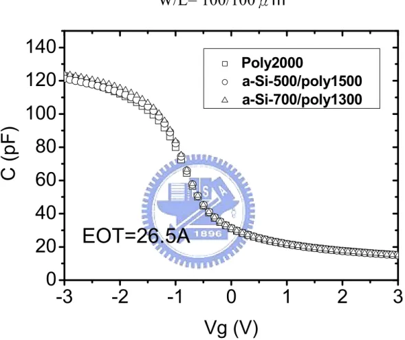
shown in Table I and Fig. 3-1. In Fig 3-2 illustrates a measured C-V profile with
different gate structures with fixed thickness of Si3N4 capping layer (CESL 1000Ǻ).
The accumulation capacitances in long channel devices (100 µm) are almost the same
as that of the conventional devices and the EOT is about 26.5Ǻ. The dependence of
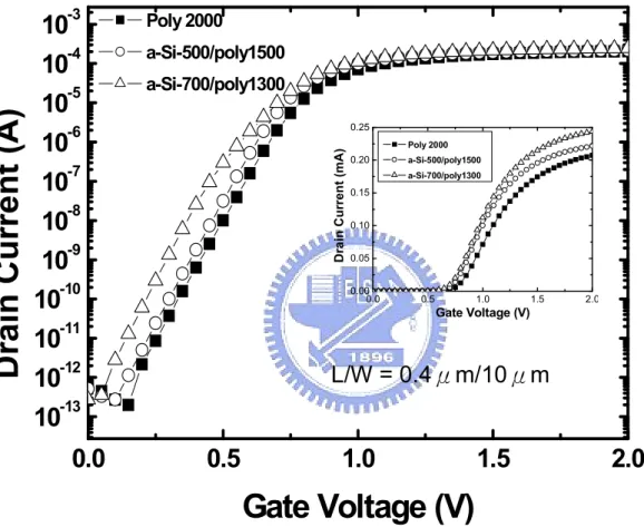
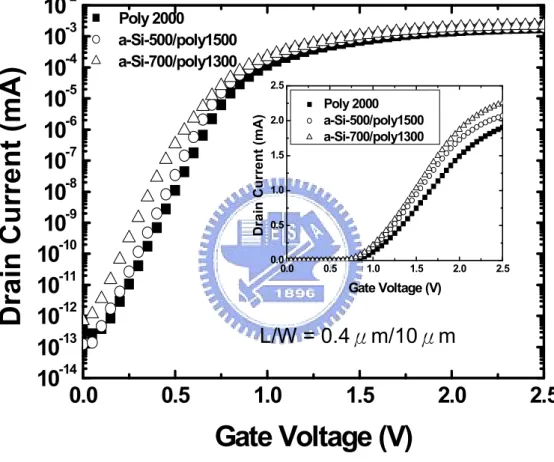
Id-Vg characteristics was measured at Vd = 0.1V on different thickness of amorphous
(a-Si) layer are shown in Fig. 3-3. The dependence of Id-Vg characteristics is
measured at Vd = 1V on different thickness of a-Si layer is shown in Fig. 3-4. The
improvement of current (linear curve) drivability is in proportion to thickness of a-Si
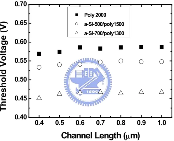
and would not decrease Ioff current in all samples. Fig. 3-5 and Fig. 3-6 show the
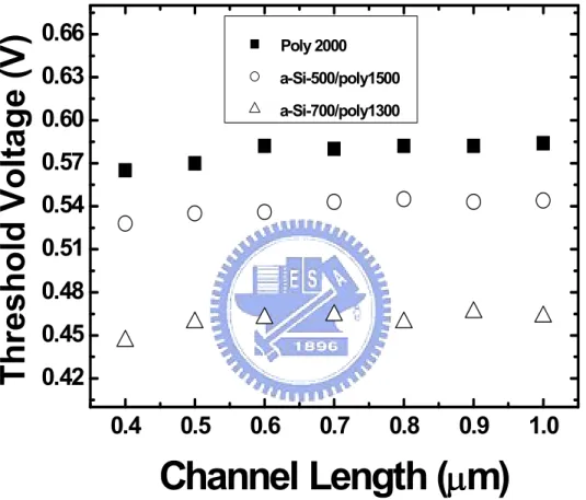
threshold voltages (measured at Vd = 0.1V or Vd = 1V) of the device with a-Si layers
of different thicknesses. The threshold voltage is proportional to the thickness of a-Si
layer. The a-Si stack layers increasing that Vth is small than control sample. We
conjecture this is related to the bandgap narrowing effect caused by the channel strain
Barrier Lowing) effect among all samples. Fig. 3-8 shows the transconductance (Gm)
increases with the increase of thickness of a-Si layer. The a-Si-700/poly-Si sample can
improve 14.5% compare to control sample in the channel length at 0.4µm. This result
implies that the strain dependence on mobility enhancement by stack of a-Si gate
structure. The mechanism of the stress elevation could be as follows: before the
dopant activation process, the stacked gate is in amorphous phase due to the bottom
a-Si and high dose implantation of arsenic on top of poly-Si. The recrystallization of
amorphous region during the rapid thermal annealing step leads to the shrinkage of
total thickness of stacked a-Si gate [29] and results in the residual compressive stress.
Therefore, the compressive stress in the stacked gate provides additional high-tensile
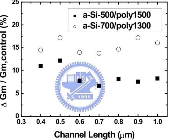
strain to the channel region. Fig. 3-9 represents the a-Si-500/poly-Si and
a-Si-700/poly-Si samples compare to the control sample Poly-2000 that the Gm
enhancement percentage with different channel length. We can see that the Gm
enhancement reaches 8 ~ 12% at the channel length between 1um to 0.4µm in the
a-Si-500/poly-Si sample. For the a-Si-700/poly-Si split, it is seen that the Gm
enhancement reaches 14 ~ 17.5%. The dependence of output characteristics on
different thickness of a-Si layer is shown in Fig. 3-10. The drain current of
nMOSFETs with a-Si-700/poly-Si showed 12% and a-Si-500/poly-Si shows 6%
a-Si-700/poly-Si sample that the drive current enhancement reaches 10~15% and
a-Si-500/poly-Si enhancement reaches 5~9% compared to the control sample at the
channel length between 1um to 0.4 µm. It is very interesting since the improvement of
current drivability and Gm increase as thickness on a-Si layer is increased. This may
be due to the thicker a-Si layer when re-crystallization during rapid thermal annealing
Table. I Gate structure with fixed Si
3N
4for local strained channel devices.
Si
3N
4-capping layer
Gate structure
Si
3N
41000Ǻ
Poly-2000
V
a-Si-500/Poly-1500
V
a-Si-700/Poly-1300
V
(a)Poly 2000 (b)a-Si-500/Poly1500
(c) a-Si-700/Poly1300.
Fig. 3-1 Gate structure with different condition (a)Poly 2000 (b)a-Si-500/Poly1500
(c) a-Si-700/Poly1300.
W/L= 100/100μm
Fig. 3-2 C-V characteristics for different thickness of a-Si layer.
-3
-2
-1
0
1
2
3
0
20
40
60
80
100
120
140
C
(p
F
)
Vg (V)
Poly2000
a-Si-500/poly1500
a-Si-700/poly1300
EOT=26.5A
Fig. 3-3 I
d-V
gcharacteristics for different thickness of a-Si layer.
0.0 0.5 1.0 1.5 2.0 0.00 0.05 0.10 0.15 0.20 0.25 Poly 2000 a-Si-500/poly1500 a-Si-700/poly1300 D ra in C u rr e n t (m A ) Gate Voltage (V)L/W = 0.4μm/10μm
Id-Vg (measured at Vd = 0.1 V) for length = 0.4
μm
0.0
0.5
1.0
1.5
2.0
10
-1310
-1210
-1110
-1010
-910
-810
-710
-610
-510
-410
-3 Poly 2000 a-Si-500/poly1500 a-Si-700/poly1300D
ra
in
C
u
rr
e
n
t
(A
)
Gate Voltage (V)
Fig. 3-4 I
d-V
gcharacteristics for different thickness of a-Si layer.
Id-Vg (measured at Vd = 1 V) for length = 0.4
μm
0.0
0.5
1.0
1.5
2.0
2.5
10
-1410
-1310
-1210
-1110
-1010
-910
-810
-710
-610
-510
-410
-310
-2 Poly 2000 a-Si-500/poly1500 a-Si-700/poly1300D
ra
in
C
ur
re
nt
(
m
A
)
Gate Voltage (V)
0.0 0.5 1.0 1.5 2.0 2.5 0.0 0.5 1.0 1.5 2.0 2.5 Poly 2000 a-Si-500/poly1500 a-Si-700/poly1300 D ra in C u rr e n t (m A ) Gate Voltage (V)L/W = 0.4μm/10μm
Vt (lin) measured at Vd = 0.1 V
Fig. 3-5 Threshold voltage for different thickness of a-Si layer.
0.4
0.5
0.6
0.7
0.8
0.9
1.0
0.40
0.45
0.50
0.55
0.60
0.65
0.70
Poly 2000 a-Si-500/poly1500 a-Si-700/poly1300T
hr
e
s
hol
d
V
o
lt
a
g
e
(
V
)
Channel Length (
µ
µ
µ
µ
m)
Vt (sat) measured at Vd = 1 V
Fig. 3-6 Threshold voltage for different thickness of a-Si layer.
0.4
0.5
0.6
0.7
0.8
0.9
1.0
0.42
0.45
0.48
0.51
0.54
0.57
0.60
0.63
0.66
Poly 2000 a-Si-500/poly1500 a-Si-700/poly1300T
h
re
s
h
o
ld
V
o
lt
a
g
e
(
V
)
Channel Length (
µ
µ
µ
µ
m)
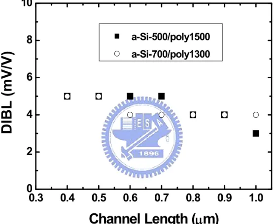
Drain Induced Barrier Lowing
Fig. 3-7 DIBL for a-Si layer with different channel length.
0.3
0.4
0.5
0.6
0.7
0.8
0.9
1.0
0
2
4
6
8
10
a-Si-500/poly1500
a-Si-700/poly1300
D
IB
L
(
m
V
/V
)
Channel Length (
µ
µ
µ
µ
m)
a-Si split+Si
3N
4-1000--Gm,length-0.4μm
Fig. 3-8 Transconductance for different thickness of a-Si layer.
0.0
0.2
0.4
0.6
0.8
0
50
100
150
200
250
300
350
400
450
Poly 2000 a-Si-500/poly1500 a-Si-700/poly1300V
gs- V
t(V)
T
ra
n
s
c
o
n
d
u
c
ta
n
c
e
(
µµµµ
S
)
L/W = 0.4μm/10μmΔGm / Gm,
control_Poly 2000(%)
Fig. 3-9 Transconductance increase versus channel length with different
thickness of a-Si layer.
0.3
0.4
0.5
0.6
0.7
0.8
0.9
1.0
0
5
10
15
20
25
∆
∆
∆
∆
G
m
/
G
m
,c
o
n
tr
o
l
(%
)
Channel Length (
µ
µ
µ
µ
m)
a-Si-500/poly1500
a-Si-700/poly1300
a-Si split+Si
3N
4-1000—I
d-V
d,length-0.4μm
Fig. 3-10 I
d-V
dcharacteristics for different thickness of a-Si layer.
0.0
0.5
1.0
1.5
2.0
2.5
0.0
5.0x10
-41.0x10
-31.5x10
-32.0x10
-32.5x10
-3 Poly 2000 a-Si-500/poly1500 a-Si-700/poly1300Id
(A)
Vd (V)
L/W = 0.4μμμμm/10μμμμm Vg-Vt = 1V Vg-Vt = 0.5V Vg-Vt = 1.5VΔI
D/ I
D,
control_Poly 2000(%)
Fig. 3-11 Saturation current increase versus channel length with different thickness
of a-Si layer. The saturation current was defined at V
G-V
th=1.5 V and V
DS= 2.5 V.
0.3
0.4
0.5
0.6
0.7
0.8
0.9
1.0
0
5
10
15
20
25
∆
∆
∆
∆
I
/
DI
D,co
n
tr
o
l
(%
)
Channel Length (
µ
µ
µ
µ
m)
a-Si-500/poly1500
a-Si-700/poly1300
Chapter 3-2 Summary of strain proximity free technique ( SPFT )
Now, we would describe the strain effect by using Strain Proximity Free Technique
(SPFT). The poly-Si gate with two different technique of the SPFT (Strain Proximity
Free Technique) and PAI (Poly Amorphous Implantation) with fixed thickness of
Si3N4 capping layer has been fabricated as shown in Table II and Fig3-12. Fig 3-13
illustrates measured C-V profile that the accumulation capacitance in long channel
devices (100 µm) is almost the same as that of the conventional devices and the EOT
is about 26.5 Ǻ. The dependence of Id-Vg characteristics with Vd = 0.1V with
different technique of poly gate is shown in Fig. 3-14. The dependence of Id-Vg
characteristics was measured at Vd = 1V on different technique of poly gate is shown
in Fig. 3-15. The improvement of current (linear curve) drivability by using SPFT and
PAI_SPFT technique was enhanced. In Fig. 3-16 and Fig. 3-17 show the threshold
voltages were measured at Vd = 0.1V and Vd = 1V with different techniques. It found
the threshold voltage has slight roll-off characteristics among the devices and the
control sample describes a pronounced reverse short channel effect (RSCE). By using
SPFT and PAI _SPFT technique, the Vth are smaller than control sample. This is
related to the bandgap narrowing effect caused by the channel strain. Fig 3-18
indicates there are no significant differences of DIBL (Drain Induced Barrier Lowing)
PAI_SPFT technique. The SPFT sample improves 19% and the PAI_SPFT sample
improves 21% compare to control sample in the channel length as 0.35 µm. A simple
model is presented to explain the mechanism of PAI_SPFT technique. As in Ref.
[30-31], it was reported that the vertical compressive stress is the major part of stress
in SMT process. However, SPFT process and conventional SMT technique are
different as the implant process. From the report [28] that it is very interesting in
SMT2 sample which was fabricated with high temperature stress memorization during
the final RTA-requires differential process, but not necessarily S/D amorphization. It
found the SMT2 sample in NMOS saturated drive current improve 20%. The SMT2
sample process is similar to the SPFT technique. We advance simple model to explain
the mechanism of SPFT technique. The polysilicon film is a temperature dependent
elastic-plastic material [31]. When increasing temperature the polysilicon is elastic
upto the yielding point and then is plastic beyond the yielding point [32]. The
polysilicon in plastic region will cause residual strain and deformation, as showed in
Fig. 3-20. During the RTA process, the changes in the poly silicon film microstructure
re-crystallization and grain change can account for some of the stress variation
[33-34]. In our sample the poly-silicon grain size with SPET process and without
SPFT is compared by AFM and SEM in Fig. 3-21 and Fig. 3-22. Mean grain size for
to 72nm. There is possibility that grain size changes during SPET process may induce
tensile stress memorization phenomena in the channel region [35]. It will provide a
high vertical compressive strain on poly-Si after RTA process and a residual strain
will be induced in poly-Si. This mechanism could be explained the stress elevation by
using SPFT to enhance electron mobility. In Fig. 3-23, as the gate length is scaling the
percentage increase of Gm with the SPFT and PAI_SPFT samples compared to the
control sample. Fig. 3-24 shows the drain current enhancement reaches 13% in the
SPFT samples and 15% in the PAI_SPFT samples compare to the control samples at a
channel length of 0.35 µm. As the gate length is scaling the percentage increase of
drive current of the SPFT and PAI_SPFT samples compared to the controls sample in
SPFT process
Table. II Poly gate with SPFT and PAI_SPFT technique.
split
Gate structure
PAI
(S:As / E:10kev
/ D:1E15)
Si
3N
4(1500
Ǻ)
RTA
(1050
oC)
Remove
Si
3N
4Poly 2000
Poly 2000
V
V
V
Poly 2000
V
V
V
V
P well
P-type
LOCOS SiO2 LOCOS
Poly 2000
(a) Poly 2000 (b) Poly 2000+Si
3N
4+RTA
(c) Poly 2000+PAI+Si
3N
4+RTA (d) process flow
Fig. 3-12 Poly gate with SPFT and PAI_SPFT technique (a) Poly 2000
W/L= 100/100μm
Fig. 3-13 C-V characteristics for SPFT and PAI_SPFT technique.
-3
-2
-1
0
1
2
3
0
20
40
60
80
100
120
140
C
(
p
F
)
Vg (V)
Poly 2000
Poly 2000_SPFT
Poly 2000_PAI_SPFT
EOT=26.5A
EOT=26.5A
Fig. 3-14 I
d-V
gcharacteristics for SPFT and PAI_SPFT technique.
Id-Vg (measured at Vd=0.1 V) for length = 0.35
μm
L/W = 0.35μμμm/10μμ μμμm
0.0
0.5
1.0
1.5
2.0
10
-1310
-1210
-1110
-1010
-910
-810
-710
-610
-510
-410
-3 Poly 2000 Poly 2000_SPFT Poly 2000_PAI _SPFTD
ra
in
C
u
rr
en
t
(A
)
Gate Voltage (V)
0.0 0.5 1.0 1.5 2.0 2.5 0.00 0.05 0.10 0.15 0.20 0.25 0.30 0.35 Poly 2000 Poly 2000_SPFT Poly 2000_PAI_SPFT D ra in C u rr e n t (m A ) Gate Voltage (V)Fig. 3-15 I
d-V
gcharacteristics for SPFT and PAI_SPFT technique.
L/W = 0.35μμμμm/10μμμμmId-Vg (measured at Vd=1 V) for length=0.35
μm
0.0 0.5 1.0 1.5 2.0 2.5 0.0 0.5 1.0 1.5 2.0 2.5 3.0 Poly 2000 Poly 2000_SPFT Poly 2000_PAI_SPFT D rain C u rren t ( m A ) Gate Voltage (V)
0.0
0.5
1.0
1.5
2.0
2.5
10
-1310
-1210
-1110
-1010
-910
-810
-710
-610
-510
-410
-310
-2 Poly 2000 Poly 2000_SPFT Poly 2000_PAI _SPFTD
ra
in
C
u
rr
e
n
t
(A
)
Gate Voltage (V)
Vt (lin) measured at Vd=0.1 V
Fig. 3-16 Threshold voltage for SPFT and PAI_SPFT technique.
0.4 0.6 0.8 1.0 0.52 0.53 0.54 0.55 0.56 0.57 0.58
Poly 2000
Poly 2000_SPFT
Poly 2000_PAI_SPFT
T
h
re
s
h
o
ld
V
o
lt
a
g
e
(
V
)
Vt (sat) measured at Vd=1 V
Fig. 3-17 Threshold voltage for SPFT and PAI_SPFT technique.
0.4
0.6
0.8
1.0
0.52
0.53
0.54
0.55
0.56
0.57
0.58
Poly 2000
Poly 2000_SPFT
Poly 2000_PAI_SPFT
T
h
re
s
h
o
ld
V
o
lta
g
e
(V
)
(a) Poly 2000 (b) Poly 2000_SPFT
(c) Poly 2000_PAI_SPFT (d) DIBL for SPFT and PAI_SPFT.
Fig. 3-18 DIBL for SPFT and PAI_SPFT technique.
0.0 0.5 1.0 1.5 2.0 2.5 1E-13 1E-12 1E-11 1E-10 1E-9 1E-8 1E-7 1E-6 1E-5 1E-4 1E-3 Vg (V) Id ( A ) 0.0 0.5 1.0 1.5 2.0 2.5 1E-13 1E-12 1E-11 1E-10 1E-9 1E-8 1E-7 1E-6 1E-5 1E-4 1E-3 Id (A ) Vg (V) 0.0 0.5 1.0 1.5 2.0 2.5 1E-13 1E-12 1E-11 1E-10 1E-9 1E-8 1E-7 1E-6 1E-5 1E-4 1E-3 Id (A ) Vg (V) 0.4 0.6 0.8 1 0 2 4 6 8 10 Poly 2000 Poly 2000+SPFT Poly 2000+PAI+SPFT D IB L ( m V /V )
Channel Length (um)
Vd=0.1v
Vd=0.1v
Vd=1v
Vd=1v
Swing=85.1mv/dec
Swing=85 mv/dec
Swing=85mv/dec
Vd=0.1v
Vd=1v
Fig. 3-19 Transconductance for SPFT and PAI_SPFT technique.
L/W = 0.35μm/10μm
21%
0.0
0.2
0.4
0.6
0.8
0
100
200
300
400
500
Poly 2000
Poly 2000_SPFT
Poly 2000_PAI_SPFT
Tr
a
ns
c
on
duc
ta
nc
e
(
µµµµ
S
)
V
gs- V
t(V)
(a) AFM image for Poly 2000 sample. (b) 3-D AFM image for Poly 2000 sample.
(c) AFM image for Poly 2000_SPFT sample (d) 3-D AFM image for Poly 2000_SPFT sample.
Fig. 3-21 AFM image for Poly 2000 sample and Poly 2000_SPFT sample.
Poly 2000 sample mean grain size is 94 nm and Poly 2000_SPFT sample
mean grain size is 72 nm.
(b) SEM image for Poly 2000_SPFTsample.
Fig. 3-22 SEM image for Poly 2000 and Poly 2000_SPFT samples. The grain size is
between 77 nm and 106 nm in Poly 2000 sample and grain size is between 64 nm and
79 nm in Poly 2000_SPFT sample.
ΔGm / Gm,
control_Poly 2000(%)
Fig. 3-23 Transconductance increase versus channel length with SPFT and
PAI_SPFT technique.
0.4
0.6
0.8
1.0
0
4
8
12
16
20
Poly2000_SPFT
Poly2000_PAI_SPFT
∆
∆
∆
∆
G
m
/
G
m
,c
o
n
tr
o
l
(%
)
Channel Length (
µ
µ
µ
µ
m)
Poly 2000 split_Si
3N
4-1000—I
d-V
d,length-0.35μm
Fig. 3-24 I
d-V
dcharacteristics for SPFT and PAI_SPFT technique.
L/W = 0.35μμμμm/10μμμμm Vg-Vt = 0.5V Vg-Vt = 1V Vg-Vt = 1.5V 0.0 0.5 1.0 1.5 2.0 2.5 0.0 5.0x10⁻⁴ 1.0x10⁻³ 1.5x10⁻³ 2.0x10⁻³ 2.5x10⁻³ 3.0x10⁻³ Poly 2000 Poly 2000_SPFT Poly 2000_PAI_SPFTId
(
A
)
Vd (V)
Δ
Δ
Δ
ΔI
D/ I
D,
control_Poly 2000(%)
Fig. 3-25 Saturation current increase versus channel length with SPFT and
PAI_SPFT technique. The saturation current was defined at V
G-V
th=1.5 V
and V
DS= 2.5 V.
0.3
0.4
0.5
0.6
0.7
0.8
0.9
1.0
1.1
0
2
4
6
8
10
12
14
16
Poly 2000_SPFT
Poly 2000_PAI_SPFT
∆
∆
∆
∆
I
/
DI
D,c
o
n
tr
o
l
(%
)
µ
µ
µ
µ
Chapter 3-3 Summary of stacked a-Si gate structure with SPFT
In this section we would describe the local strained technique by using stacked a-Si
gate structure with SPFT. The dependence of Id-Vg and transconductance
characteristics with SPFT and a-Si-700/poly1300_SPFT gate structure technique are
shown in Fig. 3-26. It found that the SPFT can further increase Gm 16% compare to
the control sample. Moreover, the Gm increases 23% could be achieved when
a-Si-700/poly1300_SPFT gate structure. The mechanism of the stress enhancement in
stacked a-Si-700/poly1300 gate could be as follows: the re-crystallization of
amorphous region during SPFT process leads to shrinkage of total thickness of
stacked a-Si/poly-Si gate and results in the residual tensile strain to channel. The
stacked gate structure with optimization of a-Si/poly-Si thickness will provide more
vertical compressive stress and longitudinal tensile stress into channel region. By
using SPFT process and a-Si-700/poly1300_SPFT gate structure that the Vth is small
than the control sample, as showed in Fig. 3-27. The shift of Vth may cause to the
bandgap narrowing effect caused by the channel strain. In Fig. 3-28, as the gate length
is scaling the percentage increase of transconductance of the SPFT and
a-Si-700/poly1300_SPFT gate structure compared to the control sample. Fig. 3-29
shows the drain current enhancement reaches 11% in the SPFT and 16% in
of 0.4 µm. As the gate length is scaling the percentage increase of drive current of the
SPFT and a-Si-700/poly1300_SPFT gate structure samples compared to the control
Fig. 3-26 Id-Vg and transconductance characteristics with SPFT and
a-Si-700/poly1300_SPFT gate structure.
L/W = 0.4μμμm/10μμ μμm μ
Id-Vg (measured at Vd=0.1 V) for length=0.4
μm
0.0
0.5
1.0
1.5
2.0
1E-13
1E-12
1E-11
1E-10
1E-9
1E-8
1E-7
1E-6
1E-5
1E-4
1E-3
0
100
200
300
400
500
600
Tr
a
ns
c
o
nduc
ta
n
c
e
(
µµµµ
S
)
Poly 2000 Poly 2000_SPFT a-Si-700/poly1300_SPFTD
ra
in
C
ur
re
nt
(A
)
Gate Voltage (V)
Vt (linear) measured at Vd=0.1 V
Fig. 3-27 Threshold voltage for SPFT and a-Si-700/poly1300_SPFT gate
structure .
0.4
0.5
0.6
0.7
0.8
0.9
1.0
0.44
0.46
0.48
0.50
0.52
0.54
0.56
0.58
0.60
Poly 2000 Poly 2000_SPFT a-Si-700/poly1300_SPFTT
h
re
s
h
o
ld
Vo
lt
a
g
e
(
V)
Channel Length(um)
Δ
Δ
Δ
ΔGm / Gm,
control_Poly 2000(%)
Fig. 3-28 Transconductance increase versus channel length with SPFT
and a-Si-700/poly1300_SPFT gate structure.
0.4
0.5
0.6
0.7
0.8
0.9
1.0
0
5
10
15
20
25
∆
∆
∆
∆
G
m
/
G
m
,c
o
n
tr
o
l
(%
)
Channel Length (
µ
µ
µ
µ
m)
Poly 2000_SPFT
a-Si-700/poly1300_SPFT
Gate split_Si
3N
4-1000—I
d-V
d,length-0.4μm
Fig. 3-29 I
d-V
dcharacteristics for SPFT and a-Si-700/poly1300_SPFT
gate structure.
L/W = 0.4μμμμm/10μμμμm Vg-Vt = 0.5V Vg-Vt = 1V Vg-Vt = 1.5V0.0
0.5
1.0
1.5
2.0
2.5
0.0
5.0x10
-41.0x10
-31.5x10
-32.0x10
-32.5x10
-33.0x10
-3 Poly 2000 Poly 2000_SPFT a-Si-700/poly1300 _SPFTId
(A
)
Vd (V)
ΔI
D/ I
D,
control_Poly 2000(%)
Fig. 3-30 Saturation current increase versus channel length with SPFT and
a-Si-700/poly1300 _ SPFT gate structure. The saturation current was defined at
V
G-V
th=1.5 V and V
DS= 2.5 V.
0.4
0.5
0.6
0.7
0.8
0.9
1.0
0
5
10
15
20
∆
∆
∆
∆
I
/
DI
D,c
o
n
tr
o
l
(%
)
Channel Length (
µ
µ
µ
µ
m)
Poly 2000_SPFT
a-Si-700/poly1300_SPFT
3-4 Hot carrier reliability
One of the serious reliability problems posed by continued shrinking of MOSFETs
into the submicron regime is the hot-carrier effect . If device channel length in scaling
and the power-supply voltage remains constant, the internal lateral electric field is
increasing so much. This would cause the inversion layer charge acquire energy (or a
high effective temperature, thus called hot carriers) enough to impact ionization that
generates electron-hole pairs in silicon (as shown in Fig. 3-31), and leads to a number
of harmful devices phenomena. The most important hot carrier effect is the damage
inflicted to the gate oxide and Si/SiO2 interface. This causes a time dependent
degradation of various MOSFET characteristics, for example, threshold voltage,
linear region transconductance, subthreshold slope (swing), and saturation current.
The substrate current of the SPFT and PAI_ SPFT samples with various channel
lengths are shown in Fig. 3-32. It significant seen the SPFT sample substrate current
is much larger than the control sample with reducing channel length. And PAI_SPFT
sample substrate current has slightly larger than SPFT sample at the same channel
length. In Fig. 3-33, the a-Si-700/poly1300_SPFT sample substrate current is larger
than the other splits with reducing channel. The results indicates that the channel
strain enhance mobility and impact ionization rate [36-37]. An empirical expression
for substrate current is Isub α exp (-φi / qλE), whereλ is the mean-free path of
which is shown to be about the magnitude of the bandgap [38-39]. Therefore, the
bandgap narrowing will act on substrate current. In Fig. 3-34 shown the substrate
current with three splits of samples at Vds = 3.5 V and channel length is 0.35um. The
devices were stressed at Vds = 3.5 V and VGS at maximum substrate current. The
Id-Vg and transconductance characteristics with three samples at Vds=0.1 V were
measured before and after stress 5000 seconds as shown in Fig. 3-35. The stress
degradation caused by the hot electrons. We found that the shift of threshold voltage (ΔVth) and degraded peak transconductance (ΔGm) are slightly higher in SPFT
sample as a function of the stress time. This result is attributed by improving drain
current and induced higher substrate current, as shown in the inset in Fig. 3-36 and
Fig. 3-37. In Fig. 3-38 shown the substrate current with another three splits, hot
carrier were stressed at Vds = 3.5 V and VGS at Isub max, the Id-Vg and
transconductance characteristics were measured at Vds = 0.1V before and after stress
5000 seconds. We found that the shift of threshold voltage (ΔVth) higher in SPFT
sample as a function of the stress time (shown in Fig. 3-39). But degraded peak
transconductance (ΔGm) higher in a-Si-700/poly1300 _ SPFT sample as shown in
SiO2
Poly
e
-e
-e
-h
+h
+h
+I
subFig. 3-31 Schematic showing electron-hole pairs generation by impact
ionization due to hot electrons.
S D
Vg > 0
Vd > Vg Vs = 0
Fig. 3-32 Substrate current versus gate voltage with the three splits in
different channel lengths of 0.4, 0.7, 1.0 µm.
L = 1
µm
L = 0.7µm
L = 0.4µm
0
1
2
3
4
0.00
0.05
0.10
0.15
0.20
S
u
b
s
tr
a
te
C
u
rr
e
n
t
(m
A
)
Vg (V)
Poly 2000 Poly 2000_SPFT Poly 2000_PAI_SPFTFig. 3-33 Substrate current versus gate voltage with SPFT and
a-Si/poly1000_SPFT splits in different channel lengths of 0.4, 0.7, 1.0
µm.
L = 0.4µm
L = 0.7µm
L = 1µm
0 1 2 3 40.00
0.05
0.10
0.15
0.20
S
u
b
s
trat
e
C
u
rr
en
t
(m
A
)
Gate Voltage (V)
Poly 2000 Poly 2000_SPFT a-Si-700/poly1300_SPFT(a) Substrate current (b) Before and after 5000s hot
electron stress for the control
sample.
(c) Before and after 5000s hot electron (d)Before and after stress 5000s
stress hot electron stress for the SPFT stress hot electron stress for the
sample. PAI_SPFT sample.
Fig. 3-34 Hot carrier stress for the three splits at Vds=3.5v &
Vg=Isub_max .
0.0 0.5 1.0 1.5 2.0 10-13 10-12 10-11 10-10 10-9 10-8 10-7 10-6 10-5 10-4 10-3 0 100 200 300 400 500 600 700 T ra n s c o n d u c ta n c e ( µµµµ S ) D ra in C u rre n t (A ) Gate Voltage (V) fresh stress_10s stress_100s stress_200s stress_500s stress_1000s stress_2000s stress_3000s stress_5000s 0.0 0.5 1.0 1.5 2.0 10-13 10-12 10-11 10-10 10-9 10-8 10-7 10-6 10-5 10-4 10-3 0 100 200 300 400 500 600 700 T ra n s c o n d u c ta n c e (µµµµ S ) fresh stress_10s stress_100s stress_200s stress_500s stress_1000s stress_2000s stress_3000s stress_5000s D ra in C u rr e n t (A ) Gate Voltage (V) 0.0 0.5 1.0 1.5 2.0 10-13 10-12 10-11 10-10 10-9 10-8 10-7 10-6 10-5 10-4 10-3 0 100 200 300 400 500 600 700 fresh stress_10s stress_100s stress_200s stress_500s stress_1000s stress_2000s stress_3000s stress_5000s T ra n s c o n d u c ta n c e ( µµµµ S ) D ra in C u rr e n t (A ) Gate Voltage (V) Poly 2000_SPFT Poly 2000 Poly 2000_PAI_SPFT W/L=10/0.35 um W/L=10/0.35 um W/L=10/0.35 um W/L=10/0.35 um 0.0 0.5 1.0 1.5 2.0 2.5 3.0 3.5 0.00 0.01 0.02 0.03 0.04 0.05 0.06 S u b s tr a te C u rr en t (m A ) Gate Voltage (V) Poly 2000 Poly 2000_SPFT Poly 2000_PAI_SPFT0.0
0.5
1.0
1.5
2.0
10
-1310
-1210
-1110
-1010
-910
-810
-710
-610
-510
-410
-3 0 100 200 300 400 500 600 700T
ra
n
sco
n
d
u
ct
an
ce
(
µµµµ
S
)
D
rain
Cu
rr
en
t
(A
)
Gate Voltage (V)
Poly 2000 Poly 2000_SPFT Poly 2000_PAI_SPFT W/L=10/0.35 um fresh stress_5000sFig. 3-35 Subthreshold and transconductance characteristics for
the SPFT and PAI_SPFT samples before and after stress 5000 sec.
Fig. 3-36 Channel hot carrier characteristics for SPFT and
PAI_SPFT samples.
W/L=10/0.35µ
m1000
2000
3000
4000
5000
0
20
40
60
80
100
120
D
e
lta
V
th
(m
V
)
Stress Time (sec)
Poly 2000
Poly 2000_SPFT
Poly 2000_PAI_SPFT
Fig. 3-37 Channel hot carrier characteristics for SPFT and
PAI_SPFT samples.
W/L=10/0.35 um1000
2000
3000
4000
5000
0
-5
-10
-15
-20
-25
-30
Poly 2000
Poly 2000_SPFT
Poly 2000_PAI_SPFT
D
e
lta
G
m
/G
m
(%
)
(a) (b)
(c) (d)
Fig. 3-38 Before and after hot carrier stress 5000 sec for the three splits at
Vds=3.5v & Vg=Isub_max .(a) Substrate current (b) Poly 2000 sample (c)
Poly 2000_SPFT sample (d) a-Si-700/poly1300_SPFT sample.
0.0 0.5 1.0 1.5 2.0 10-13 10-12 10-11 10-10 10-9 10-8 10-7 10-6 10-5 10-4 0 100 200 300 400 T ra n s c o n d u c ta n c e ( µµµµ S ) D ra in C rre n t (A ) Gate Voltage (V) fresh stress_10s stress_100s stress_500s stress_1000s stress_3000s stress_5000s 0.0 0.5 1.0 1.5 2.0 10-13 10-12 10-11 10-10 10-9 10-8 10-7 10-6 10-5 10-4 0 100 200 300 400 500 fresh stress_10s stress_100s stress_500s stress_1000s stress_3000s stress_5000s T ra n s c o n d u c ta n c e ( µµµµ S ) D ra in C u rr e n t (A ) Gate Voltage (V) 0.0 0.5 1.0 1.5 2.0 10-13 10-12 10-11 10-10 10-9 10-8 10-7 10-6 10-5 10-4 0 100 200 300 400 500 600 D ra in C u rr e n t (A ) Gate Voltage (V) fresh stress_10s stress_100s stress_500s stress_1000s stress_3000s stress_5000s T ra n s c o n d u c ta n c e ( µµµµ S ) W/L=10/0.4 um W/L=10/0.4 um W/L=10/0.4 um
Fig. 3-39 Channel hot carrier characteristics for SPFT and
a-Si-700/poly1300 _ SPFT samples.
0
1000
2000
3000
4000
5000
0
20
40
60
80
100
D
e
lt
a
V
th
(m
V
)
Stress Time (sec)
Poly 2000
Poly 2000_SPFT
a-Si-700/poly1300_SPFT
Fig. 3-40 Channel hot carrier characteristics for SPFT and
a-Si-700/poly1300 _ SPFT samples.
W/L=10/0.4 um1000
2000
3000
4000
5000
0
-10
-20
-30
-40
-50
Poly 2000
Poly 2000_SPFT
a-Si-700/poly1300_SPFT
D
e
lta
G
m
/G
m
(%
)
Stress Time (s)
Summary and Conclusion
In summary, we have proposed strain proximity free technique (SPFT) in
nMOSETs, it could be solve etch processes problems with dense structure in logic
CMOS circuit. We found that the transconductance (GM) exhibits an 16% increase and
drain current improve 10% at channel length 0.4μm of nMOFETs with SPFT and the
hot carrier stress would not serious damage. A multiple strain-gate engineering that
utilizes the SPFT and a stacked a-Si/poly-Si gate structure. The GM and current
drivability could be improved by controlling the SPFT process and the thickness of
stacked gate structure. Without the limitation of stressor volume in high density
CMOS circuits, we believe this scheme, by using both SPFT and stacked a-Si/poly-Si
gate structure will provide us a guide line to keep continuous improvement in future
References:
[1] B. W. Bush, O. Pluchery, Y. J. Chabal, D. A. Muller, R. L. Opila, K. J. Raynien, and E. Garfunkel, “Materials characterization of alternative gate dielectrics,” MRS bulletin (MRS bull.), pp. 206-211, 2002.
[2] C. S. Lai, W. C. Wu, T. S. Chao, J. H. Chen, J. C. Wang, L. L. Tay, and N. Rowell, “Suppression of Interfacial Reaction for HfO2 on Silicon by Pre-CF4 Plasma Treatment,” Appl. Phys. Lett., vol.89, p. 072904, 2006.
[3] S. W. Hung, and J. G. Hwu, “Lateral Nonuniformity of Effective Oxide Charges in MOS Capacitors with Al2O3 Gate Dielectrics,” IEEE Trans. Electron Devices, vol. 53, pp. 1608-1614, 2006.
[4] R. People, “Physics and applications of GexSi1−x/Si strained layer heterostructue ,” IEEE J. Quantum Electron, vol. 22, pp. 1696–1710, Sept. 1986.
[5] J. J. Welser, J. L. Hoyt, and J. F. Gibbons, “Electron mobility enhancement in strained-Si n-type metal-oxide-semiconductor field-effect transistors,” IEEE Electron Device Lett., vol. 15, pp. 100–102, Mar. 1994.
[6] J. Welser, J. L. Hoyt, S. Takagi, and J. F. Gibbons, “Strain dependence of the performance enhancement in strained-Si n-MOSFETs,” IEDM Tech. Dig, 1994, pp. 373–376.
[7] M. V. Fischetti and S. E. Laux, “Band structure, deformation potentials, and carrier mobility in strained-Si, Ge, and SiGe alloys,” J. Appl. Phys. vol. 80, no. 4, pp. 2234–2252, 1996.
[8] D. K. Nayak, K. Goto, A. Yutani, J Murota, and Y. Shiraki, “High-Mobility Strained-Si PMOSFETs,” IEEE Trans. Electron Devices, Vol. 43, pp. 1709-1716, Oct. 1996.
[9] T. Manku and A. Nathan, “Energy band structure for strained p-type Si1−xGex ,” Phys. Rev. B, Condens. Matter, vol. 43, no. 15, pp. 12634–12637, May 15, 1991. [10] M. L. Lee, E. A. Fitzgerald, M. T. Bulsara, M. T. Currie, and A. Lochtefeld,
“Strained Si, SiGe, and Ge channels for high-mobility metal oxide semiconductor field effect transistors,” J. Appl. Phys, 2005.
[11] D. K. Nayak and S. K. Chun, “Low-field hole mobility of strained Si on (100) Si1-xGex substrate,” Appl. Phys. Lett., vol. 64, pp. 2514–2516, Jan. 1994.
[12] C. Zhi-Yuan, M.T. Currie, C.W. Leitz, G. Taraschi, E.A. Fitzgerald, J.L. Hoyt, and D.A. Antoniadis, “Electron mobility enhancement in strained-Si n-MOSFETs fabricated on SiGe-on-insulator (SGOI) substrates,” IEEE
Electron Device Lett., vol. 22, pp. 321–323, July 2001.
[13] J. R. Hwang, J. H. Ho, Y. C. Liu, J. J. Shen, W. J. Chen, D. F. Chen, W. S. Liao, Y. S. Hsieh, W. M. Lin, C. H. Hsu, H. S. Lin, M. F. Lu, A. Kuo, S. H. Lu,
![FIG. 1-2 Valence band of (a) bulk Si and (b) Si under biaxial tension.[10]](https://thumb-ap.123doks.com/thumbv2/9libinfo/8242523.171389/17.892.143.774.545.923/fig-valence-band-bulk-si-under-biaxial-tension.webp)
![Fig. 1-4 The cross sectional SEM images and stress distributions of nFET and pFET. [25]](https://thumb-ap.123doks.com/thumbv2/9libinfo/8242523.171389/18.892.197.707.125.984/fig-cross-sectional-sem-images-stress-distributions-nfet.webp)
![Fig. 1-6 Voids in the dense poly regions on STI can lead to shorts in the circuitry, when filled with tungsten contact material.[27]](https://thumb-ap.123doks.com/thumbv2/9libinfo/8242523.171389/20.892.135.783.196.541/voids-regions-shorts-circuitry-filled-tungsten-contact-material.webp)