IEEE ELECTRON DEVICE LETTERS, VOL. 21, NO. 6, JUNE 2000 289
Thickness Dependent Gate Oxide Quality of Thin
Thermal Oxide Grown on High Temperature Formed
SiGe
Y. H. Wu, Albert Chin, Senior Member, IEEE, and W. J. Chen
Abstract—For thin oxides grown on high temperature formed
Si0 3Ge0 7, the gate oxide quality is strongly dependent on oxide thickness and improves as thickness reduces from 50 to 30 Å. The thinner 30 Å oxide has excellent quality as evidenced by the compa-rable leakage current, breakdown voltage, interface-trap density and charge-to-breakdown with conventional thermal oxide grown on Si. The achieved good oxide quality is due to the high tempera-ture formed Si0 3Ge0 7that is strain relaxed and stable during ox-idation. The possible reason for strong thickness dependence may be due to the lower GeO2content formed in thinner 30 Å oxide rather than strain relaxation related rough surface or defects.
Index Terms—Gate oxide integrity, SiGe oxide, oxide reliability.
I. INTRODUCTION
H
IGH quality thin gate oxide [1]–[3] is urgently required for SiGe p-MOSFET’s [4]–[10] , although higher hole mobility and better current drive capability than standard Si counterpart are demonstrated. To avoid strain relaxation in SiGe, gate oxide is generally formed by a low temperature process [11] using plasma CVD deposition, but the quality is unable to compare with conventional thermal SiO . On the other hand, high temperature oxide directly grown on SiGe has poor quality because the strain relaxation not only reduces hole mobility [10] but also generates rough surface and defects [8]–[10]. The low temperature process also prohibits SiGe from using in deep sub- m devices with high-K dielectrics [12], [13]. Recently, we developed a high temperature formed Si Ge [14] using the similar process as silicidation [15]. Because SiGe is formed by high temperature rapid-thermal-an-nealing (RTA) and solid-phase epitaxy (SPE), better thermal stability can be expected. Therefore, high temperature (950 C) RTA can be used to achieve the important low junction-leakage [11] of p n source and drain after implantation [16]. Because of the high Ge content, good hole mobility of 250 cm /Vs is still obtained [16] that is two times higher than Si even without the strain [17]. In this work, we have studied thin gate oxides grown on high temperature formed SiGe. The gate oxide quality improves and becomes comparable with standard SiO as thickness reduces from 50 to 30 Å. Possible reason for thisManuscript received July 23, 1999; revised January 17, 2000. This work was supported by the NSC of Taiwan, R.O.C., under Contract 88-2215-E-009-032. The review of this letter was arranged by Editor T.-J. King.
Y. H. Wu and A. Chin are with the Department of Electronics Engineering, National Chiao Tung University, Hsinchu 300, Taiwan, R.O.C.
W. J. Chen is with the Department of Mechanical Materials Engineering, Na-tional Yun-Lin Polytechnic Institute, Huwei, Taiwan, R.O.C.
Publisher Item Identifier S 0741-3106(00)04712-1.
improvement may be due to the lower GeO content inside the thinner 30 Å oxide.
II. EXPERIMENTAL
To avoid any B diffusion though thin gate oxide, p-type Si wafers were used instead of n-type wafers although SiGe should be applied to p-MOSFET’s. After device isolation, Si Ge was formed in the active region by RTA and SPE at 900 C from deposited amorphous Ge layer. The native oxide is specially taken care of using HF-vapor passivation [13]–[16] before Ge deposition. More detailed Si Ge forming process and ma-terial characterization can be found elsewhere [14]. Gate oxides of 30 and 50 Å were grown by dry oxygen at 900 C for both Si Ge and Si control sample. The oxide thickness is mea-sured by ellipsometer and TEM. Gate capacitors were formed after a 3000 Å poly-Si deposition and subsequent process steps.
III. RESULTS ANDDISCUSSION
Fig. 1(a) and (b) show the current–voltage (I–V) characteris-tics of 50 and 30 Å thermal oxides formed on both Si Ge and standard Si, respectively. For control 50 and 30 Å SiO , a breakdown electric field of MV/cm is obtained that is the typical value for thermal SiO on Si. For 50 Å oxide grown on Si Ge ,three to four times higher leakage current and 1 V lower breakdown voltage than control SiO are observed. In sharp contrast, comparable leakage current and breakdown voltage with control SiO are obtained for Å thermal oxide grown on Si Ge . The smaller leakage current of thermal oxide grown on Si Ge than Si is due to the 1 Å thicker ness. The trend of improved oxide quality with thinner thick-ness is important for deep sub- m devices where the gate oxide thickness is continuously scaling down.
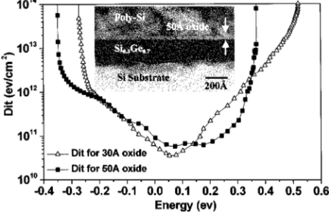
We have used capacitance–voltage C–V and TEM to further investigate the oxide quality. Important interface-trap density ( ) can be obtained from high and low frequency C–V curves. Fig. 2 shows the and cross-sectional TEM of SiGe thermal oxides. Although very low of and
eV /cm is measured for respective 30 Å and 50 Å oxides, this difference is small. The low may be due to very smooth interface and uniform oxide thickness observed by TEM. Therefore, the strong thickness dependence on oxide quality is irrelevant to strain relaxation related rough interface or defect generation. This is due to the high temperature formed Si Ge that is already strain relaxed and stable during
290 IEEE ELECTRON DEVICE LETTERS, VOL. 21, NO. 6, JUNE 2000
Fig. 1. I–V characteristics of (a) 50 and (b) 30 Å thermal oxides formed on
both Si Ge and standard Si.
Fig. 2. Interface trap density for 30 and 50 Å oxide grown on high temperature formed Si Ge . Inset figure is the cross-sectional TEM of 50 Å SiGe thermal oxide on Si Ge .
dation. Furthermore, no dislocation penetration into underneath Si is observed that also explains the low leakage current.
We have further analyzed the SiGe oxides by SIMS. Fig. 3(a) and (b) shows the SIMS profiles of 50 and 30 Å SiGe oxides, respectively. In both cases, a Ge snow plowing is observed in oxide–SiGe interface. For 50 Å SiGe oxide, in addition to the Ge pileup at interface, another Ge peak at Å below surface is also found. Similar phenomenon is also reported for oxide
Fig. 3. SIMS profiles of (a) 50 and (b) 30 Å thermal oxides grown on high temperature formed Si Ge .
Fig. 4. Charge-to-breakdown (Q ) distribution of thermal oxides grown on Si Ge and Si after a 4.5 V stress.
grown on Si Ge [18]. In contrast, no such additional peak can be observed for thinner 30 Å SiGe oxide. The possibility of additional Ge peak less than 15 Å below surface is low, although this small distance is near the limitation of SIMS. At such small distance close to surface, Ge may have high probability of out-diffusion because of the high oxidation temperature. Therefore, the improved oxide quality of 30 Å SiGe oxide may be due to the smaller content of weaker GeO inside the SiO .
WU et al.: THIN THERMAL OXIDE GROWN ON HIGH TEMPERATURE FORMED SiGe 291
To further evaluate the 30 Å SiGe oxide, we have also inves-tigated the oxide reliability. Fig. 4 shows the charge-to-break-down ( ) distribution for both thermal SiGe oxide and SiO under 4.5 V stress. An average of 0.12 C/cm is ob-tained for control thermal SiO that is close to reported value. Good SiGe oxide reliability can be evidenced by the high of 0.11 C/cm that is comparable with thermal SiO . The good reliability is related to the high temperature stable Si Ge that has a uniform electric field distribution resulted from the smooth surface and interface.
IV. CONCLUSION
Improved oxide quality is observed with decreasing thickness of thermal oxide grown on high temperature formed Si Ge . We have achieved comparable oxide quality with thermal SiO for thinner 30 Å oxide.
REFERENCES
[1] G. Q. Lo, W. Ting, J. Ahn, and D. L. Kwong, “Improved performance and reliability of MOSFET’s with ultrathin gate oxides prepared by con-ventional furnace oxidation of Si in Pure N O Ambient,” in Symp. VLSI
Tech., 1991, pp. 43–44.
[2] C. T. Liu, “Circuit requirement and integration challenges of thin gate dielectrics for ultra small MOSFETs,” in IEDM Tech. Dig., 1998, pp. 747–750.
[3] A. Chin et al., “The effect of native oxide on thin gate oxide integrity,”
IEEE Electron Device Lett., vol. 19, pp. 426–428, Nov. 1998.
[4] D. K. Nayak et al., “Wet oxidation of GeSi strained layers by rapid thermal processing,” Appl. Phys. Lett., vol. 57, pp. 369–371, 1990. [5] P. W. Li et al., “SiGe pMOSFET’s with gate oxide fabricated by
mi-crowave electron cyclotron resonance plasma processing,” IEEE
Elec-tron Device Lett., vol. 15, pp. 402–405, Oct. 1994.
[6] K. Ismail, “Si/SiGe CMOS: Can it extend the limitation of Si?,” in
ISSCC Tech. Dig., 1997, pp. 116–117.
[7] S. P. Voinigescu, C. A. T. Salama, J. P. Noel, and T. I. Kamins, “Opti-mized Ge channel profiles for VLSI compatible Si/SiGe p-MOSFET’s,” in IEDM Tech. Dig., 1994, pp. 369–372.
[8] S. Verdonckt-Vandebroek et al., “SiGe-channel heterojunction p-MOSFET’s,” IEEE Trans. Electron Devices, vol. 41, pp. 90–101, Jan. 1994.
[9] K. Goto et al., “Fabrication of a Si Ge channel metal-oxide-semi-conductor field-effect transistor (MOSFET) containing high Ge fraction layer by low-pressure chemical vapor deposition,” Jpn. J. Appl. Phys., vol. 32, pp. 438–441, 1993.
[10] R. S. Prassad, T. J. Thornton, S. Kanjanachuchai, J. Fernandez, and A. Matsumura, “Mobility degradation in gated Si:SiGe quantum wells with thermally grown oxide,” Electron Lett., vol. 31, pp. 1876–1878, 1995. [11] Y. Taur and T. K. Ning, Fundamental Modern VLSI
De-vices. Cambridge, U.K.: Cambridge Univ. Press, 1998, p. 286. [12] S. C. Song et al., “Ultra thin (20Å) CVD Si N gate dielectric for
deep-sub-micron CMOS devices,” in IEDM Tech. Dig., 1998, pp. 373–376.
[13] A. Chin et al., “Device and reliability of high-K Al O gate dielectric with good mobility and low D ,” in Proc. Symp. VLSI Tech., 1999, pp. 135–136.
[14] Y. H. Wu, W. J. Chen, A. Chin, and C. Tsai, “The effect of native oxide on epitaxial SiGe from deposited amorphous Ge on Si,” Appl. Phys. Lett., vol. 74, pp. 528–530, 1999.
[15] Y. H. Wu et al., “Improved electrical characteristics of CoSi using HF-vapor pretreatment,” IEEE Electron Device Lett., vol. 20, pp. 200–202, May 1999.
[16] Y. H. Wu, W. J. Chen, A. Chin, and C. Tsai, “Electrical and structure characterization of single crystalline SiGe formed by Ge deposition and RTP,” in Proc. 41st Electronic Materials Conf., Santa Barbara, CA, 1999.
[17] T. Manku and A. Nathan, “Lattice mobility of holes in strained and un-strained Si Ge alloys,” IEEE Electron Device Lett., vol. 12, pp. 704–706, Dec. 1991.
[18] H. K. Liou, P. Mei, U. Gennser, and E. S. Yang, “Effect of Ge con-centration on SiGe oxidation behavior,” Appl. Phys. Lett., vol. 10, pp. 1200–1202, 1991.