國 立 交 通 大 學
電子工程學系 電子研究所
博 士 論 文
互補式金氧半積體電路之系統層級靜電放電
防護設計
SYSTEM-LEVEL ESD PROTECTION DESIGN IN
CMOS ICS WITH TRANSIENT DETECTION
CIRCUITS
研 究 生:顏承正(Cheng-Cheng Yen)
指導教授:柯明道(Ming-Dou Ker)
互補式金氧半積體電路之系統層級靜電放電
防護設計
SYSTEM-LEVEL ESD PROTECTION DESIGN IN
CMOS ICS WITH TRANSIENT DETECTION
CIRCUITS
研 究 生:顏承正
Student: Cheng-Cheng Yen
指導教授:柯明道
Advisor: Ming-Dou Ker
國 立 交 通 大 學
電子工程學系電子研究所
博 士 論 文
A Dissertation
Submitted to Department of Electronics Engineering &
Institute of Electronics
College of Electrical and Computer Engineering
National Chiao Tung University
in Partial Fulfillment of the Requirements
for the Degree of Doctor of Philosophy
in
Electronics Engineering
April 2009
Hsinchu, Taiwan, Republic of China
互補式金氧半積體電路之系統層級靜電放電
防護設計
研究生:顏承正
指導教授:柯明道 博士
國立交通大學電子工程學系電子研究所
摘要
在互補式金氧半積體電路中,系統層級靜電放電測試(System-Level ESD Test)已成 為一個重要的可靠度問題。由於日益複雜的積體電路功能,如混合式信號(Mix-Signal) 電路、多重電源供應系統(Multiple Power Supplies)、射頻(Radio Frequency, RF)電路、系 統單晶片(System on Chip)等等,使得積體電路元件所處的環境會受到來自元件內部或外 部的雜訊干擾,因此這些雜訊會隨機地出現在積體電路產品的電源、接地、輸入/輸出 腳位(Pin)上,使積體電路產品較以往更容易受到雜訊干擾的威脅。隨著半導體元件尺寸 的 微 縮 , 過 去 的 研 究 已 經 證 實 在 系 統 層 級 靜 電 放 電 測 試 以 及 快 速 暫 態 脈 衝 測 試 (Electrical Fast Transient Test)之下,暫態的干擾訊號會使寄生在互補式金氧半導體積體 電路中的矽控整流器(Silicon ControlledRectifier, SCR)產生閂鎖效應。由系統層級靜電放 電測試所引起的可靠度問題來自於多功能整合型的積體電路設計,以及嚴格的法規要 求。在系統層級靜電放電測試的規格中(IEC 61000-4-2),一個擁有積體電路的電子設備 在接觸放電(Contact-Discharge)及空氣放電(Air-Discharge)測試模式中如欲達到“等級四 "的標準需求,則此待測設備(Equipment Under Test, EUT)必須通過高達±8kV(接觸放電 模式)及±15kV(空氣放電模式)的靜電放電等級需求。
在傳統的解決方法中,會在電子產品的印刷電路板上增加離散元件(Discrete Component)抑制暫態雜訊的干擾,包括利用反耦合電容(Decoupling Capacitor)、Ferrite
Choke、暫態突波抑制器(Transient Voltage Suppressor)、限流電阻(Current-Limiting Resistance)、防護板(Shielding Plate)等,皆能在印刷電路板抑制對積體電路產品所產生 的暫態雜訊干擾,但是這些額外增加的離散元件會大幅增加電子產品的成本。因此在以 積體電路方式提出相關的解決方案,設計出符合高階系統層級靜電放電測試規格以及減 少離散元件使用的電子產品,將會為工業界所急切需求。 有鑒於此,本論文將針對用於系統層級靜電放電防護所需的暫態偵測電路積體電 路設計進行研究分析。主要的研究方向包括:(1) 評估不同電源匯流排之間的靜電放電 箝制電路(Power-Rail ESD Clamp Circuit)結構對於系統層級靜電放電測試的耐受度,(2) 在快速脈衝測試時暫態觸發閂鎖效應的物理機制,(3) 評估各種面板層級(Board-Level) 雜訊濾波器對抑制暫態觸發閂鎖效應的效用,(4) 暫態偵測電路積體電路設計方法(IC Design Methodology),以及(5) 暫態數位轉換器積體電路設計方法。 本論文第二章首先評估不同電源匯流排之間的靜電放電箝制電路(Power-Rail ESD Clamp Circuit)結構對於系統層級靜電放電測試以及快速暫態脈衝測試的耐受度。在本論 文中,發現在電源匯流排之間的靜電放電箝制電路結構中具有鎖存迴授迴路以及串接 PMOS 迴授迴路電路架構容易產生似閉鎖效應(Latchup-Like Failure)之故障出現,在系
統層級靜電放電以及快速暫態脈衝測試過後,在電源(VDD)與地端(VSS)之間導致巨大電 流通過,容易使積體電路產品因過大電流而損毀。相較於以三級反相器為主的靜電放電 箝制電路架構,該具有鎖存迴授迴路以及串接 PMOS 迴授迴路的電源匯流排之間的靜 電放電箝制電路架構較易發生類似閂鎖效應(Latchup-Like Failure)之故障狀況。本論文 中提出一個結合鎖存迴授迴路以及利用 NMOS 產生回復功能的新電源匯流排之間的靜 電放電箝制電路結構,經實驗晶片驗證,本研究所提出的電源匯流排間靜電放電箝制電 路結構可成功避免類似閂鎖效應的觸發,以及具有高箝制能力且能節省佈局面積,可應 用在全晶片之靜電放電防護設計上。 本論文第三章針對在快速暫態脈衝測試時造成暫態觸發閂鎖效應的物理機制加以 探討分析。經由相關的實驗量測驗証,本論文發現快速暫態脈衝測試將導致一種電壓振 幅會隨時間遞減的脈衝震盪電壓產生於積體電路的電源腳位上。此種電壓會使儲存於積 體電路內的少數載子(Minority Carrier)快速移動,進一步形成“掃回電流(Sweep-Back Current)"而引發暫態觸發閂鎖效應。本論文所提出的實驗驗證提供實用的研究分析工 具,以期能進一步發展出能有效防止暫態觸發閂鎖效應的電路設計技巧、佈局(Layout) 準則、以及半導體製程技術。為了能更進一步地提升積體電路對暫態觸發閂鎖效應的防
護能力,本論文更評估了不同面板層級雜訊濾波器對抑制暫態觸發閂鎖效應的實際效 用。這些雜訊濾波元件包括電容濾波器、電容-電感濾波器(LC-Like)、π形濾波器、亞 鐵鹽珠(Ferrite Bead)、暫態突波抑制器(Transient Voltage Suppressor, TVS)、及混合式濾 波器等。藉由這些雜訊濾波元件反耦合(Decouple)或吸收因快速暫態脈衝測試在積體電 路電源(地)端造成的瞬間雜訊,則積體電路對抑制暫態觸發閂鎖效應的防護能力將可有 效提升。所得到的實驗結果可提供印刷電路板(Printed Circuit Board, PCB)設計者一個有 用的參考準則,以期能利用適當的雜訊濾波器來有效提升積體電路對暫態觸發閂鎖效應 的防護能力。
本論文第四章是在 0.18-μm 3.3-V CMOS 製程技術中,所實現的暫態偵測電路
(Transient detection Circuit)。此偵測電路是利用閉鎖電路的架構來設計,利用 HSPICE 軟體所提供的正弦波以及阻尼因子(Damping Factor)的參數設定,可成功模擬並量化暫 態偵測電路在系統層級靜電放電以及快速暫態脈衝測試時的工作情形。電路系統的模擬 狀態包括了在電源線與地線上的同步干擾,或因為電路板繞線差異或待測元件擺放位置 不同而造成在電源線與地線之間的非同步干擾情形,以及在各種不同製程參數下對於暫 態偵測電路的影響。此暫態偵測電路在系統層級靜電放電或是快速暫態脈衝發生時,可 偵測出發生在電源線上的暫態干擾訊號並紀錄之,並配合韌體或軟體設定,使電路在受 到電磁干擾而故障時,能送出重新啟動訊號(Reset)使系統自動作回復的動作。此暫態偵 測電路可整合至 CMOS 晶片中,並可結合韌體的使用,以提升待測電子產品對系統層 級靜電放電以及快速暫態脈衝測試的防護能力。 本論文第五章是在0.18-μm 1.8-V CMOS 製程技術中,所實現的暫態偵測電路。此 偵測電路是利用反相器電路架構以及電阻電容延遲效應來設計,利用HSPICE 軟體所提 供的正弦波以及阻尼因子(Damping Factor)的參數設定,可成功模擬並量化此暫態偵測 電路在系統層級靜電放電以及快速暫態脈衝測試時的工作情形。此暫態偵測電路在系統 層級靜電放電或是快速暫態脈衝發生時,已成功驗證可偵測出發生在電源線上的暫態干 擾訊號並紀錄之,使電子產品在受到電磁干擾而故障時,可配合韌體或軟體設定送出重 新啟動訊號(Reset)使系統自動作回復的動作。
本論文第六章是結合暫態偵測電路以及積體電路濾波電路(On-Chip Noise Filter Network),發展完全整合於積體電路上(Full Integrated Circuit)能輸出數位編碼訊號的暫 態數位轉換器(Transient-to-Digital Converter)。在系統層級靜電放電測試時,暫態數位轉 換器所輸出的數位編碼訊號會對應不同電壓準位的暫態突波。在整體系統的設計上,利
用結合韌體(Firmware)的系統設計,制定出具有執行自動恢復功能的整體系統規劃。當 有快速變化且具有低電壓準位的暫態突波發生時,暫態數位轉換器會送出低位元數位編 碼訊號,可做為韌體執行部分系統自動重新恢復(Partial System Auto-Recovery)的指標 (Index),指標訊號可暫存於韌體中,並經由回授程式的不斷檢測,直至暫態突波的影響 消失為止。當有快速變化且具有低電壓準位的暫態突波發生時,暫態數位轉換器會送出 高 位 元 數 位 編 碼 訊 號 , 可 做 為 韌 體 執 行 全 部 系 統 自 動 重 新 恢 復(Total System Auto-Recovery)的指標。因此,利用結合暫態數位轉換器以及韌體的系統規劃的設計方 式,以期增進顯示電子產品對系統規格靜電放電的全晶片防護能力。 以上針對用於系統層級靜電放電測試的積體電路設計方法,快速暫態脈衝測試造 成的暫態閂鎖效應特性,以及暫態偵測電路晶片設計,本論文所進行的相關研究皆有實 際晶片量測,並有相對應的國際會議及期刊論文發表。
SYSTEM-LEVEL ESD PROTECTION DESIGN IN CMOS ICS
WITH TRANSIENT DETECTION CIRCUITS
Student: Cheng-Cheng Yen Advisor: Dr. Ming-Dou Ker
Department of Electronics Engineering and Institute of Electronics
National Chiao-Tung University
Abstract
System-level electrostatic discharge (ESD) events have become a primary reliability issue in CMOS integrated circuit (IC) products. With more and more complicated design of integrated circuits, such as mixed-signal, mixed-voltage, system-on-chip (SOC), etc, CMOS devices will suffer more electrical transient noises coming from environment and the interior of CMOS ICs. With advanced semiconductor technology of scaled clearance between PMOS and NMOS devices, it has been proven that such electrical transient noises can cause transient-induced latchup (TLU) failure on the inevitable parasitic silicon controlled rectifier (SCR) in CMOS ICs under system-level ESD and electrical fast transient (EFT) tests. The reliability issue of system-level ESD events results from not only the progress of more integrated functions into a single chip but also from the strict requirements of reliability test standards, such as the system-level ESD test standard of IEC 61000-4-2. The microelectronic products must sustain the ESD level of ±8kV (±15kV) under contact-discharge (air-discharge) test mode to achieve the immunity requirement of “level 4” in the IEC 61000-4-2 test standard.
The additional noise filter networks, such as the magnetic core, capacitor filter, ferrite bead (FB), transient voltage suppressor (TVS), RC filters, are often used to improve the system-level ESD immunity of microelectronic products. The system-level ESD immunity of CMOS ICs under system-level ESD test can be significantly enhanced by choosing proper
noise filter networks. However, the additional discrete noise-bypassing components substantially increase the total cost of microelectronic products. Therefore, the chip-level solutions to meet high system-level ESD specification for microelectronic products without additional discrete noise-decoupling components on the microelectronic products are highly desired by IC industry.
This dissertation focuses on the chip-level solutions for the system-level ESD protection design. Several major topics including: (1) investigation on the latchup-like failure of power-rail ESD clamp circuits under system-level ESD tests, (2) clarification of TLU physical mechanism under EFT tests, (3) evaluations of board-level noise filters to suppress TLU, (3) proposed on-chip transient detection circuits, and (5) proposed transient-to-digital converters.
In chapter 2, four power-rail ESD clamp circuits with different ESD-transient detection circuits were fabricated in a 0.18-μm CMOS process and tested to compare their system-level ESD and EFT susceptibility, which are named as power-rail ESD clamp circuits with typical RC-based detection, PMOS feedback, NMOS+PMOS feedback, and cascaded PMOS feedback in this work. During the system-level ESD and EFT tests, where the ICs in a system have been powered up, the feedback loop used in the power-rail ESD clamp circuits provides the lock function to keep the ESD-clamping NMOS in a “latch-on” state. The latch-on ESD-clamping NMOS, which is often drawn with a larger device dimension to sustain high ESD level, conducts a huge current between the power lines to perform a latchup-like failure after the system-level ESD and EFT tests. A modified power-rail ESD clamp circuit is proposed to solve this problem. The proposed power-rail ESD clamp circuit can provide high enough chip-level ESD robustness, and without suffering the latchup-like failure during the system-level ESD and EFT tests.
In chapter 3, the occurrence of TLU in CMOS ICs under the EFT tests is studied. The test chip with the parasitic SCR structure fabricated by a 0.18-μm CMOS process was used in the EFT tests. For physical mechanism characterization, the specific “sweep-back” current caused by the minority carriers stored within the parasitic PNPN structure of CMOS ICs is the major cause of TLU under EFT tests. Different types of board-level noise filter networks are evaluated to find their effectiveness for improving the immunity of CMOS ICs against TLU under EFT tests. By choosing proper components in each noise filter network, the TLU immunity of CMOS ICs against EFT tests can be greatly improved.
and EFT protection are proposed in this work. The circuit performance to detect positive and negative electrical transients under system-level ESD and EFT testing conditions has been investigated by the HSPICE simulation and verified in silicon chip. The experimental results have confirmed that the proposed on-chip transient detection circuit can successfully memorize the occurrence of the system-level ESD and EFT events. The detection output of proposed on-chip transient detection circuits can be used as the firmware index to execute system recovery procedure to provide a hardware/firmware co-design to improve the immunity of CMOS IC products against electrical transient disturbance.
In chapter 5, a new on-chip transient detection circuit for electrical fast disturbance protection design is proposed in this work. The circuit performance to detect different positive and negative ESD-induced or EFT-induced transient disturbance has been investigated by the HSPICE simulation and verified in silicon chip. The EFT generator combined with attenuation network and capacitive coupling clamp has been used as the evaluation method to verify the detection function of the proposed on-chip transient detection circuit under EFT tests. The test chip in a 0.18-μm CMOS process with 1.8-V devices has confirmed that the proposed on-chip transient detection circuit can successfully detect and memorize the occurrence of the transient disturbance under system-level ESD or EFT tests.
In chapter 6, a novel on-chip transient-to-digital converter composed of four RC-based transient detection circuits and four different RC filter networks has been successfully designed and verified in a 0.18-μm CMOS process with 3.3-V devices. The output digital thermometer codes of the proposed on-chip transient-to-digital converter correspond to different ESD voltages under system-level ESD tests. These output digital codes can be used as the firmware index to execute different auto-recovery procedures in microelectronic systems. Thus, the proposed on-chip transient-to-digital converter can be further combined with firmware design to provide an effective solution to solve the system-level ESD and EFT protection issue in microelectronic systems equipped with CMOS ICs.
Chapter 7 summarizes the main results of this dissertation. Some suggestions for the future works are also addressed in this chapter.
Acknowledgment
感謝柯明道教授的指導與專業領域上的訓練。感謝交通大學吳重雨校
長、晶焱科技姜信欽博士、奇景光電陳東暘博士、中山大學王朝欽教授、
交通大學吳介琮教授、交通大學蘇朝琴教授在百忙之中抽空擔任我的口試
委員,並給予珍貴的指導與建議,讓此博士論文更加完整。
感謝任職於奇景光電的蔡志忠技術長、陳東暘博士鼎力協助實驗晶片下
線與研究工作進行,使本論文的研究成果得以成功驗證,並順利發表於國
際期刊與國際研討會。
感謝實驗室的陳世倫博士、許勝福博士、陳榮昇博士、張瑋仁博士、蕭
淵文博士、陳世宏博士、徐振洲學長
、
羅文裕學長
、黃鈞正學長
、阿傑、
祖德、豪哥、瑋明、羅怡凱、台祐、二師兄、邱大人、范振麟
、霸子、金
毛、智閔、與陳穩義、賴泰翔、王資閔、林群祐、邱柏硯、蔡惠雯、弼嘉、
莊介堯、俊哥、蒙神、鯉魚、世範、小州哥、佳琪、翁怡歆、林宛彥等同
學與學弟妹們在研究與生活上的協助與扶持,尤其在我心情低落時,很多
人給我許多鼓勵。感謝任職於晶焱科技的賢哥、阿貴、
志豪哥
、小李、小
黑、阿方、蔡耀城學長
、
子平學長給我的許多幫助與支持
。
特別感謝學弟
廖期聖在晶片設計與製作上的用心與努力,可以使相關的研究順利進行。
爸爸開刀期間,謝謝蕭淵文博士常常幫我處理投稿的論文。口試前一個月
來回新竹台北加護病房,謝謝陳穩義、小胖、小州哥、佳琪幫我處理口試
準備的事情,我很珍惜大家幫助過我的一切,謝謝你們。此外,感謝實驗
室助理卓慧貞小姐在行政事務上的許多協助。
謝謝新竹馬偕醫院洗腎室的醫師與護士照料長期洗腎的父親。謝謝淡水
馬偕的羅鈺華護理師,台北振興醫院開刀房的小英,慈濟大林醫院的嬋芳,
高雄榮總的雅婷,在爸爸各地看診期間給予的幫助跟關懷。我要特別感謝
新竹東區扶輪社以及耳鼻喉科林安復醫師,在生活上以及醫療上給予我們
的幫助,在面對許多洗腎的併發病症以及被診斷出鼻咽腫瘤時,林醫師細
心幫爸爸看診並給予我們建議與協助,許多畫面至今令我感動以及難忘。
由衷感謝敬愛的父親顏色先生、母親黎柑妹女士、姊姊顏承真小姐、姊
夫曾明育先生、兩位可愛的外甥女圓元跟詣琁。感謝親人的支持、陪伴與
照顧,讓我順利完成學業。感謝所有幫助我、陪伴我一同成長的師長、長
輩、朋友、學長姊、同學、學弟妹們,願大家平安喜樂。
顏 承 正
誌於竹塹交大
九十八年 春
Contents
Abstract (Chinese)
iAbstract (English)
vContents
ixTable Captions
xiiiFigure Captions
xvChapter 1. Introduction
11.1. Background 1 1.2. Issue of Transient Disturbance Events 1
1.2.1. System-Level ESD Tests 1
1.2.2. Electrical Fast Transient (EFT) Tests 8
1.3. System to Overcome Electrical Transient Disturbance 13 1.3.1. Traditional Board-Level Solutions 13 1.3.2. Hardware/Firmware System Co-Design Solution 14
1.4. Organization of This Dissertation 15
Chapter 2. Investigation and Design of On-Chip Power-Rail ESD Clamp
Circuits Without Suffering Latchup-Like Failure During
System-Level
ESD
and
EFT
Tests
18 2.1. Background 18 2.2. Power-Rail ESD Clamp Circuits 20
2.2.1. With Typical RC-Base Detection 22 2.2.2. With Direct PMOS Feedback 23 2.2.3. With NMOS+PMOS Feedback 23 2.2.4. With Cascaded PMOS Feedback 24 2.2.5. Realization in Silicon Chip 25
2.3. Experimental Results and Discussion 27
2.3.1. TLU Tests 28
2.3.3. EFT Tests 28
2.4. Modified Power-Rail ESD Clamp Circuit 45
2.4.1. Circuit Structure 46
2.4.2. Simulation Analysis 46
2.4.3. Experimental Results 47
2.4.3.1. Turn-On Verification 47
2.4.3.2. TLU Tests 49
2.4.3.3. System-Level ESD Tests 50
2.4.3.4. EFT Tests 51
2.4.3.5. Chip-Level ESD Robustness 53
2.5. Conclusion 55
Chapter 3. Transient-Induced Latchup in CMOS Integrated Circuits
under EFT Tests
563.1. Background 56
3.2. SCR Test Structure 59
3.3. Experimental Results and Discussion 62 3.3.1. TLU Tests with EFT Generator 63
3.3.2. Physical Mechanism 66
3.4. Evaluation on Board-Level Noise Filters to Suppress Latchup
under EFT Tests 67 3.4.1. Capacitor Filter, LC-Like Filter, and π-Section Filter 68 3.4.2. Ferrite Bead, TVS, and Hybrid Type Filters 70
3.4.3. Discussion 72
3.5. Conclusion 73
Chapter 4. On-Chip Transient Detection Circuit Design for Electrical
Transient Disturbance Protection (Scheme I)
74
4.1. Background 74 4.2. Transient Detection Scheme I Deigned with 1.8-V Devices 75 4.3. HSPICE Simulation Results 76
4.3.1. System-Level ESD Zapping Condition 76
4.3.2. EFT Zapping Condition 82
4.4. Experimental Results 86
4.4.1. TLU Tests 86
4.4.2. System-Level ESD Tests 88
4.4.3. EFT Tests 91
4.4.3.1 With Attenuation Network 91 4.4.3.2 With Capacitance Coupling Clamp 93
4.5. Hardware/Firmware System Co-Design Application 95
4.6. Conclusion 97
Chapter 5. On-Chip Transient Detection Circuit Design for Electrical
Transient Disturbance Protection (Scheme II)
985.1. Background 98
5.2. Transient Detection Scheme II Deigned with 1.8-V Devices 99
5.3. HSPICE Simulation Results 100
5.3.1. System-Level ESD Zapping Condition 100
5.3.2. EFT Zapping Condition 102
5.4. Experimental Results 105
5.4.1. TLU Tests 105
5.4.2. System-Level ESD Tests 107
5.4.3. EFT Tests 109
5.4.3.1 With Attenuation Network 109 5.4.3.2 With Capacitance Coupling Clamp 111
5.5. Conclusion 113
Chapter 6. On-Chip Transient-to-Digital Converter
1146.1. Background 114
6.2. Evaluation on Board-Level Noise Filter Networks 115 6.2.1. Board-Level Noise Filter Networks 116 6.2.2. Experimental Results of System-Level ESD Tests 117
6.3. Transient detection Circuit Designed with Noise Filter Network 120
6.3.1. On-Chip Noise Filter Network 120 6.3.2. Experimental Results of System-Level ESD Tests 120
6.4. On-Chip Transient-to-Digital Converter 122
6.4.1. Circuit Structure 123
6.4.2. System-Level ESD Tests 124
6.4.3. EFT Tests 127
6.5. Applications in CMOS ICs with Firmware Co-Design 131
6.6. Conclusion 133
Chapter 7. Conclusions and Future Works
1347.1. Specific New Results of This Dissertation 134
7.2. Future Works 135
References
136Vita
142Table Captions
Chapter 1
Table 1.1 Waveform Parameters of System-Level ESD Discharge Current 5
Table 1.2 Component-Level ESD Specifications 5
Table 1.3 Levels of System-Level ESD Test 6
Table 1.4 Recommended Classifications of System-Level ESD Test Results 6
Table 1.5 Characteristics of the EFT Generator 8
Table 1.6 Characteristics of the Fast Transient/Burst 9
Table 1.7 Characteristics of a Single EFT Voltage Pulse 9
Table 1.8 Levels of EFT Test 12
Table 1.9 Output Voltage Peak (VP) Values and Repetition Rates under EFT Test 12
Chapter 2
Table 2.1 Comparison on the Susceptibility among Four Different Power-Rail ESD Clamp
Circuits Under TLU Test 32
Table 2.2 Comparison on the Susceptibility among Four Different Power-Rail ESD Clamp Circuits Under System-Level ESD Test 38
Table 2.3 Comparison on the Susceptibility among Four Different Power-Rail ESD Clamp
Circuits Against EFT Test 43
Table 2.4 Comparison on TLU Levels Between Proposed Power-Rail ESD Clamp Circuit with NMOS Reset Function and the Original Power-Rail ESD Clamp Circuit With NMOS+PMOS Feedback Under TLU Test 50
Table 2.5 Comparison on the Susceptibility Between Proposed Power-Rail ESD Clamp Circuit with NMOS Reset Function and the Original Power-Rail ESD Clamp Circuit With NMOS+PMOS Feedback Under System-Level ESD Test 50
with NMOS Reset Function and the Original Power-Rail ESD Clamp Circuit With NMOS+PMOS Feedback Against EFT Test 53
Table 2.7 Comparison on HBM Level, CDM Level, and Layout Area among Five Different Power-Rail ESD Clamp Circuits in a 0.18-μm CMOS Process 54
Chapter 6
Table 6.1 ESD Voltage to Digital Code Characteristic of Proposed On-Chip 4-Bit
Transient-to-Digital Converter 127
Table 6.2 EFT Voltage to Digital Code Characteristic of Proposed On-Chip 4-Bit
Figure Captions
Chapter 1
Fig. 1.1 Equivalent circuit of ESD gun used in the system-level ESD test. The ESD gun has the charging (energy-storage) capacitor of 150 pF and discharge resistor of
330 Ω. 2
Fig. 1.2 Equivalent circuit of human body model (HBM) in the component-level ESD test. The charging capacitor (discharge resistor) is a smaller (larger) value of 100 pF
(1.5 kΩ). 2
Fig. 1.3 Under 8-kV ESD zapping, the peak current in system-level ESD test is about five times larger than that in component-level ESD test. 3
Fig. 1.4 Measurement instruments of system-level ESD test. 4
Fig. 1.5 Discharge electrodes of ESD gun which is used under system-level ESD test with contact discharge mode and air discharge mode. 4
Fig. 1.6 Measured VDD and VSS waveforms of the microcontroller ICs inside the keyboard
with ESD voltage of +1 kV zapping on the HCP under system-level ESD test. 7
Fig. 1.7 The equivalent circuit of EFT generator. 8
Fig. 1.8 Measured voltage waveforms under EFT tests with EFT voltage of (a) +200 V, and (b) -200 V, on 1-kΩ load with a repetition rate of 5 kHz. 10
Fig. 1.9 Measured voltage waveforms of a single pulse with EFT voltage of (a) +200 V, and (b) -200 V, on 1-kΩ load under EFT test. 11
Fig. 1.10 A traditional solution to overcome the EFT events in a keyboard product by
adding extra discrete components to absorb or bypass the electrical transients. 13
Fig. 1.11 Hardware/firmware co-design for system recovery by using the output of the
on-chip transient detection circuit. 14
Chapter 2
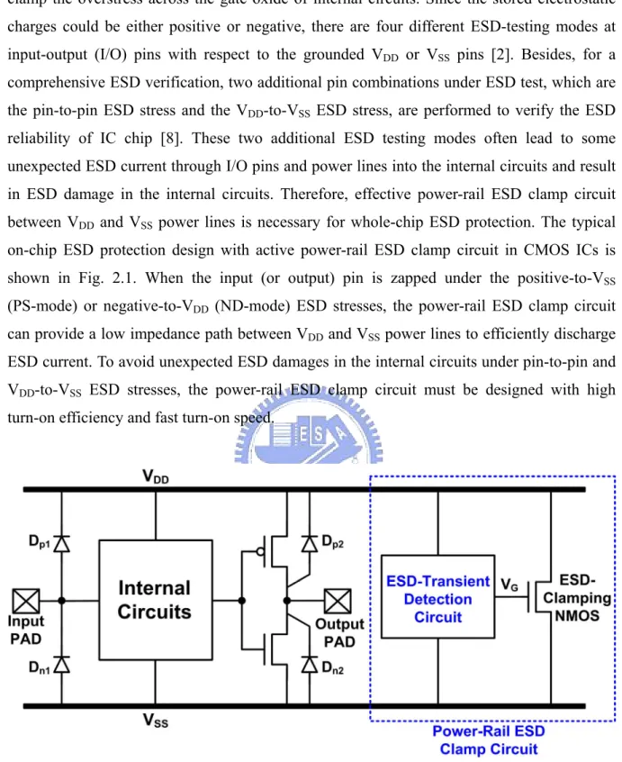
Fig. 2.1 Typical on-chip ESD protection design with active power-rail ESD clamp circuit. 19
Fig. 2.2 Four different power-rail ESD clamp circuits designed with (a) typical RC-based detection, (b) PMOS feedback, (c) NMOS+PMOS feedback, and (d) cascaded
PMOS feedback. 21
Fig. 2.3 HSPICE simulated voltage waveforms among the four different power-rail ESD clamp circuits under the VDD power-on condition. (a) A slow ramp voltage
waveform with rise time of 0.1ms is used to simulate the rising edge of the VDD
power-on voltage. (b) The simulated voltage waveforms on the node VG when the
Fig. 2.4 HSPICE simulated voltage waveforms among the four different power-rail ESD clamp circuits under HBM ESD stress condition. (a) A fast ramp voltage waveform with rise time of 10ns is used to simulate the rising edge of an HBM ESD pulse. (b) The simulated voltage waveforms on the node VG when the fast
ramp voltage is applied to VDD. 27
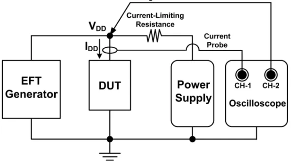
Fig. 2.5 Measurement setup for transient-induced latchup (TLU). 28
Fig. 2.6 Measured VDD and IDD waveforms on the power-rail ESD clamp circuit with
NMOS+ PMOS feedback under TLU test with VCharge of (a) -4 V, and (b) +12 V.
30
Fig. 2.7 Measured VDD and IDD waveforms on the power-rail ESD clamp circuit with
cascaded PMOS feedback under TLU test with VCharge of (a) -120 V, and (b) +700
V. 31
Fig. 2.8 Measurement setup for system-level ESD test with indirect contact-discharge test mode to evaluate the susceptibility of power-rail ESD clamp circuits. 33
Fig. 2.9 Measured VDD and IDD waveforms on the power-rail ESD clamp circuit with
typical RC-based detection under system-level ESD test with ESD voltage of (a)
-10 kV, and (b) +10 kV. 34
Fig. 2.10 Measured VDD and IDD waveforms on the power-rail ESD clamp circuit with
PMOS feedback under system-level ESD test with ESD voltage of (a) -10 kV, and
(b) +10 kV. 35
Fig. 2.11 Measured VDD and IDD waveforms on the power-rail ESD clamp circuit with
NMOS+PMOS feedback under system-level ESD test with ESD voltage of (a)
-0.2 kV, and (b) +2.5 kV. 36
Fig. 2.12 Measured VDD and IDD waveforms on the power-rail ESD clamp circuit with
cascaded PMOS feedback under system-level ESD test with ESD voltage of (a) -1
kV, and (b) +10 kV. 37
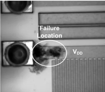
Fig. 2.13 Failure location of power-rail ESD clamp circuit after system-level ESD stress. 38 Fig. 2.14 Measurement setup for EFT test with IC power supply of 1.8 V. 39
Fig. 2.15 Measured VDD and IDD waveforms on the power-rail ESD clamp circuit with
typical RC-based detection under EFT test with EFT voltage of (a) -800 V, and (b)
+800 V. 40
Fig. 2.16 Measured VDD and IDD waveforms on the power-rail ESD clamp circuit with
PMOS feedback under EFT test with EFT voltage of (a) -800 V, and (b) +800 V. 41
Fig. 2.17 Measured VDD and IDD waveforms on the power-rail ESD clamp circuit with
NMOS+PMOS feedback under EFT test with EFT voltage of (a) -200 V, and (b) +200 V. Latchup-like failure in this EFT test. 42
Fig. 2.18 Measured VDD and IDD waveforms on the power-rail ESD clamp circuit with
cascaded PMOS feedback under EFT test with EFT voltage of (a) -200 V, and (b) +500 V. Latchup-like failure in this EFT test. 44
Fig. 2.19 Failure location of power-rail ESD clamp circuit after EFT tests. 45
Fig. 2.20 The proposed power-rail ESD clamp circuit with NMOS reset function to
overcome latchup-like failure. 46
Fig. 2.21 Measured voltage waveforms on the proposed power-rail ESD clamp circuit with
NMOS reset function in (a) ESD-stress condition and (b) power-on condition. 48
Fig. 2.22 Measured VDD and IDD waveforms on the proposed power-rail ESD clamp circuit
under TLU test with VCharge of (a) -1 kV, and (b) +1 kV. No latchup-like failure
occurs in this TLU test. 49
Fig. 2.23 Measured VDD and IDD waveforms on the proposed power-rail ESD clamp circuit
with NMOS reset function under system-level ESD test with ESD voltage of (a) -10kV and (b) +10kV. No latchup-like failure occurs in this system-level ESD test. 51
Fig. 2.24 Measured VDD and IDD waveforms on the proposed power-rail ESD clamp circuit
under EFT test with EFT voltage of (a) -800 V, and (b) +800 V. No latchup-like failure occurs in this EFT test. 52
Chapter 3
Fig. 3.1 (a) Circuit structure, and (b) device cross-sectional view of a CMOS inverter. 57
Fig. 3.2 Emission microscope (EMMI) photographs of EFT-induced TLU event in a 0.5-μm CMOS IC product with power-supply voltage of 5V. (a) Hot spots of latchup locations in the chip after EFT test, and (b) the corresponding zoomed-in latchup location, which is located across the boundary between NMOS and PMOS transistors in a digital logic block. 58
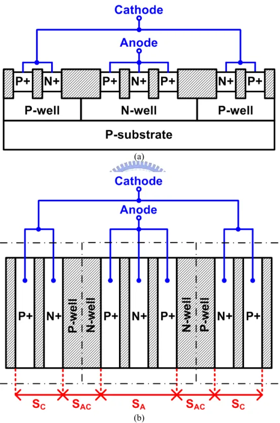
Fig. 3.3 (a) Device cross-sectional view, and (b) layout top view, of the SCR test structure
for TLU measurements. 60
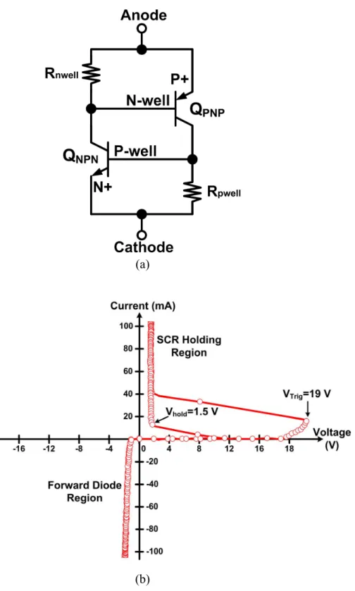
Fig. 3.4 (a) Equivalent circuit schematic of SCR device. (b) I-V characteristics of SCR device under positive and negative biases. 62
Fig. 3.5 Measurement setup for TLU under EFT tests. 63
Fig. 3.6 Measured VDD and IDD transient waveforms on SCR test structure under EFT tests
with EFT voltage of (a) -200 V, and (b) +200 V. 65
Fig. 3.7 The total stored minority carriers, QStored, causing ISb (tA≤t≤tB) inside the N-well
region. The inset figure is an ideal 1-D diode used for deriving the 1-D analytical
model of the averaged ISb (≡IAve). 67
Fig. 3.8 Measurement setup for TLU combined with noise filter network under EFT tests. 68
Fig. 3.9 Three types of noise filter network investigated for their improvements on the TLU level of the SCR. (a) Capacitor filter, (b) LC-like filter, and (c) π-section
filter. 69
three types of noise filter networks: capacitor filter, LC-like filter, and π-section
filter. 70
Fig. 3.11 Four types of noise filter networks investigated for their improvements on the
TLU level of the SCR. (a) Ferrite bead, (b) TVS, (c) hybeid type I, and (d) hybeid
type II. 71
Fig. 3.12 Relations among the TLU level of SCR, minimum impedance of ferrite bead at
25MHz, and the breakdown voltage of TVS with four types of noise filter networks: ferrite bead, TVS, hybrid type I, and hybrid type II. 72
Chapter 4
Fig. 4.1 The board-level solution for microelectronic products against electrical transient
disturbance. 75
Fig. 4.2 The proposed on-chip transient detection circuit I. 76
Fig. 4.3 Measured voltage waveforms with ESD voltage of (a) -1 kV, and (b) +1 kV. 77
Fig. 4.4 The specific time-dependent underdamped sinusoidal waveforms applied on the power and ground lines to simulate the transient disturbance under system-level
ESD zapping. 78
Fig. 4.5 Simulated VDD, VSS, VOUT1, and VOUT2 waveforms of the proposed transient
detection circuit I under system-level ESD test with larger overshooting voltage
coupled on (a) VDD, and (b) VSS. 79
Fig. 4.6 Simulated VDD, VSS, VOUT1, and VOUT2 waveforms of the proposed transient
detection circuit I under system-level ESD test with larger undershooting voltage
coupled on (a) VDD, and (b) VSS. 80
Fig. 4.7 (a) Different coupling path from the ESD zapping source to VDD and VSS pins of
CMOS IC on the PCB. (b) Time delay between the measured VDD and VSS
waveforms is due to the different coupling path. 81
Fig. 4.8 Simulated VDD, VSS, and VOUT waveforms of the proposed transient detection
circuit I under (a) positive, and (b) negative underdamped sinusoidal voltage on VDD/VSS power lines with signal delay condition. 82
Fig. 4.9 The specific time-dependent exponential pulse waveform applied on the power lines to simulate the disturbance under EFT zapping. 84
Fig. 4.10 Simulated VDD and VOUT waveforms of the proposed on-chip transient detection
circuit I under EFT tests with (a) positive, and (b) negative exponential pulse
voltage waveforms coupled on VDD. 85
Fig. 4.11 Die photo of the proposed on-chip RC-based transient detection circuits. 86
Fig. 4.12 Measurement setup for transient-induced latchup (TLU). 87
Fig. 4.13 Measured VDD and VOUT waveforms on the proposed on-chip transient detection
Fig. 4.14 Measurement setup of system-level ESD test with indirect contact discharge mode.
89
Fig. 4.15 Measured VDD and VOUT transient responses of the proposed transient detection
circuit I under system-level ESD test with ESD voltage of (a) -0.2 kV, and (b)
+0.2 kV zapping on the HCP. 90
Fig. 4.16. Measurement setup for EFT test combined with attenuation network. 91
Fig. 4.17 Measured VDD and VOUT waveforms on the proposed on-chip transient detection
circuit I under EFT tests with (a) negative, and (b) positive EFT voltages by combining with attenuation network. 92
Fig. 4.18 Measurement setup for EFT test combined with capacitive coupling clamp. 93
Fig. 4.19 Measured VDD and VOUT transient voltage waveforms of the proposed on-chip
transient detection circuit I under EFT tests with EFT voltage of (a) -200 V, and (b) +200 V by combining with capacitive coupling clamp. 94
Fig. 4.20 The hardware/firmware co-design flowchart to execute reset or recover procedures.
96
Fig. 4.21 Hardware/firmware operation during (a) power-on reset condition, and (b)
system-level ESD stress. 97
Chapter 5
Fig. 5.1 The proposed on-chip transient detection circuit II. 99
Fig. 5.2 Simulated VDD, VSS, and VOUT waveforms of the proposed transient detection
circuit II under (a) positive, and (b) negative underdamped sinusoidal voltage on
VDD/VSSpower lines. 101
Fig. 5.3 Simulated VDD and VOUT waveforms of the proposed on-chip transient detection
circuit II under EFT tests with (a) positive, and (b) negative exponential pulse
voltage waveforms coupled on VDD. 103
Fig. 5.4 Die photo of the proposed on-chip RC-based transient detection circuits. 105
Fig. 5.5 Measurement setup for transient-induced latchup (TLU). 105
Fig. 5.6 Measured VDD and VOUT waveforms on the proposed on-chip transient detection
circuit II under TLU test with VCharge of (a) +8 V, and (b) -1 V. 106
Fig. 5.7 Measurement setup of system-level ESD test with indirect contact discharge mode.
107
Fig. 5.8 Measured VDD and VOUT transient responses of the proposed transient detection
circuit II under system-level ESD test with ESD voltage of (a) +0.2 kV, and (b)
-0.2 kV zapping on the HCP. 108
Fig. 5.9 Measurement setup for EFT test combined with attenuation network. 109
circuit II under EFT tests with (a) positive, and (b) negative EFT voltages by combining with attenuation network. 110
Fig. 5.11 Measurement setup for EFT test combined with capacitive coupling clamp. 111
Fig. 5.12 Measured VDD and VOUT transient voltage waveforms of the proposed on-chip
transient detection circuit II under EFT tests with EFT voltage of (a) +200 V, and (b) -200 V by combining with capacitive coupling clamp. 112
Chapter 6
Fig. 6.1 Measurement setup for TLU combined with noise filter network under EFT tests. 115
Fig. 6.2 Four types of noise filter network investigated for their improvements on the TLU level of the SCR. (a) Capacitor filter, (b) Type-I RC filter, (c) π-section filter, and
(d) Type-II RC filter. 116
Fig. 6.3 Relations between the decoupling capacitance and the TLU level of the proposed on-chip transient detection circuit I with capacitor filter. 117
Fig. 6.4 Relations between the decoupling capacitance and the TLU level of the proposed on-chip transient detection circuit I with Type-I RC filter. 118
Fig. 6.5 Relations between the decoupling capacitance and the TLU level of the proposed on-chip transient detection circuit I with Type-II RC filter. 119
Fig. 6.6 Relations between the decoupling capacitance and the TLU level of the proposed on-chip transient detection circuit I with π-section filter. 119
Fig. 6.7 The proposed on-chip RC-based transient detection circuit combined with a noise
filter network. 120
Fig. 6.8 Die photo of the proposed on-chip RC-based transient detection circuits. 121
Fig. 6.9 Measured VDD and VOUT transient voltage waveforms of the proposed on-chip
RC-based transient detection circuit combined with a noise filter network under a system-level ESD test with an ESD voltage of (a) +1.8 kV, and (b) -1.6 kV. 122
Fig. 6.10 Proposed on-chip 4-bit transient-to-digital converter realized with four transient
detection circuits and RC filter networks. 123
Fig. 6.11 Die photo of the proposed transient-to-digital converter. 124
Fig. 6.12 Measured VOUT1, VOUT2, VOUT3, and VOUT4 transient voltage waveforms of the
proposed on-chip 4-bit transient-to-digital converter under a system-level ESD test with an ESD voltage of (a) +0.2 kV, (b) +0.4 kV, (c) +0.5 kV, and (d) +0.7 kV,
zapping on the HCP. 125
Fig. 6.13 Measured VOUT1, VOUT2, VOUT3, and VOUT4 transient voltage waveforms of the
proposed on-chip 4-bit transient-to-digital converter under a system-level ESD test with an ESD voltage of (a) -0.2 kV, (b) -0.3 kV, (c) -0.5 kV, and (d) -1.4 kV,
Fig. 6.14 The relationship between the ESD zapping voltage and the digital code in the
proposed transient-to-digital converter. 127
Fig. 6.15 Measured VOUT1, VOUT2, VOUT3, and VOUT4 transient voltage waveforms of the
proposed on-chip 4-bit transient-to-digital converter under EFT test with EFT voltage of (a) +0.7 kV, (b) +1.8 kV, (c) +2.4 kV, and (d) +3.4 kV. 128
Fig. 6.16 Measured VOUT1, VOUT2, VOUT3, and VOUT4 transient voltage waveforms of the
proposed on-chip 4-bit transient-to-digital converter under EFT test with EFT voltage of (a) -0.6 kV, (b) -0.65 kV, (c) -0.7 kV, and (d) -0.8 kV. 129
Fig. 6.17 The relationship between the EFT voltage level and the digital code in the
proposed on-chip 4-bit transient-to-digital converter. 130
Fig. 6.18 Hardware/firmware operation during (a) power-on reset condition, (b) low
Chapter 1
Introduction
In this chapter, the background and the organization of this dissertation are discussed. First, the background of transient disturbance events is introduced. Secondly, the system design solutions are discussed. Finally, the organization of this dissertation is well described.
1.1. Background
Electrical transient disturbance events have become an important reliability issue to integrated circuits (ICs). To meet the component-level ESD reliability, on-chip ESD protection circuits have been added to the I/O cells and power (VDD and VSS) cells of CMOS
ICs [1]-[8]. Besides the component-level ESD stress, electrical transient disturbance is an increasingly significant reliability issue in CMOS integrated circuit (IC) products. This tendency results from the strict requirements of reliability test standards, such as system-level ESD test for electromagnetic compatibility (EMC) regulation. In the system-level electrostatic discharge (ESD) test standard of IEC 61000-4-2 [9], the electrical/electronic product must sustain the ESD level of ±8 kV (±15 kV) under contact-discharge (air-discharge) test mode to meet the immunity requirement of “level 4.” Such high-energy ESD-induced noises often cause damage or malfunction of CMOS ICs inside the equipment under test (EUT). It has been reported that some CMOS ICs are very susceptible to electrical transient disturbance [10]-[18], even though they have passed the component-level ESD specifications such as human-body-model (HBM) of ±2 kV [19], [20], machine-model (MM) of ±200 V [21], [22], and charged-device-model (CDM) of ±1 kV [23]-[25].
1.2. Issue of Transient Disturbance Events
1.2.1. System-Level
ESD
Tests
The equivalent circuit of ESD gun used in the system-level ESD test is shown in Fig. 1.1 The ESD gun has the charging (energy-storage) capacitor of 150 pF and discharge resistor of 330 Ω. The equivalent circuit of human body model (HBM) in the component-level ESD test
is shown in Fig. 1.2 In the HBM component-level ESD test, however, the charging capacitor (discharge resistor) is a smaller (larger) value of 100pF (1.5 kΩ). Thus, compared with the ESD current in component-level ESD test, ESD current in system-level ESD test has a much larger peak current and a shorter rise time, leading to more severe damages for electronic products or their interior ICs. The ESD-induced energy can be zapped out of the mechanism with ESD gun in faster speed.
Fig. 1.1 Equivalent circuit of ESD gun used in the system-level ESD test. The ESD gun has the charging (energy-storage) capacitor of 150 pF and discharge resistor of 330 Ω.
Fig. 1.2 Equivalent circuit of human body model (HBM) in the component-level ESD test. The charging capacitor (discharge resistor) is a smaller (larger) value of 100 pF (1.5 kΩ).
Fig. 1.3 shows the typical waveforms of the discharge current under system-level ESD test (IEC 61000-4-2) and component-level ESD test (MIL-STD 883). Under 8-kV ESD zapping, the peak current in system-level ESD test is about five times larger than that in component-level ESD test. Additionally, ESD protection designs for system- and component-
level ESD tests are quite different. It has been proven [10] that a robust CMOS IC product with high component-level ESD levels could be very susceptible to the system-level ESD test. Thus, efficient ESD protection methodologies against system-level ESD events are very significant for electronic products.
Fig. 1.3 Under 8-kV ESD zapping, the peak current in system-level ESD test is about five times larger than that in component-level ESD test.
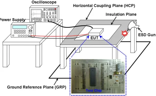
In the IEC 61000-4-2 standard [9], two test modes have been specified, which are the air-discharge test mode and the contact-discharge test mode. Contact discharge is further divided into direct discharge to the system under test, and indirect discharge to horizontal or vertical coupling planes. Fig. 1.4 shows the standard measurement setup of the system-level ESD test in the indirect contact-discharge test mode. As shown in Fig. 1.5, in the air discharge test mode, the round discharge head of ESD gun is brought close to the EUT. In the contact discharge test mode, the sharp discharge head of ESD gun is held in contact with the EUT. The measurement setup for system-level ESD test consists of a wooden table on the grounded reference plane (GRP). In addition, an insulation plane is used to separate the EUT from the horizontal coupling plane (HCP). The HCP are connected to the GRP with two 470 kΩ resistors in series. When the ESD gun zaps the HCP, the electromagnetic interference (EMI) coming from ESD will be coupled into all CMOS ICs inside EUT. The power lines of CMOS ICs inside EUT will be disturbed by the ESD-coupled energy.
Fig. 1.4 Measurement instruments of system-level ESD test [9].
Fig. 1.5 Discharge electrodes of ESD gun which is used under system-level ESD test with contact discharge mode and air discharge mode.
The object of the standard, IEC 61000-4-2 is to establish a common and reproducible basis for evaluating the performance of CMOS ICs inside the electrical/electronic microelectronic products. This standard specifies typical waveform of the discharge current, test levels, test equipment, test set-up, and test procedure. In order to verity the disturbance under system-level ESD test, the ESD gun is used to zap the ESD-induced energy into the equipment under test. In order to compare the test results in system-level ESD and component-level ESD standards, the characteristics of the waveform of discharge current are shown in Table 1.1. Table 1.2 shows the test level (test voltage) of component-level ESD test
such as human body model (HBM), machine model (MM), and charge device model (CDM) in usual condition. The system-level ESD test level with contact discharge and air discharge is shown in Table 1.3. Contact discharge is the preferred test method, and air discharge shall be used where contact discharge can’t be applied. It is not intended to imply that the test severity is equivalent between contact discharge and air discharge test methods. To compare Table 1.3 with Table 1.2, the test voltage of system-level ESD is lager than component-level ESD, no matter with contact discharge or air discharge. Noteworthiness, the voltages shown are different for each method due to the different methods of test. According to those phenomena, system-level ESD is more significant to influence the microelectronic products than component-level ESD in some situations. Table 1.4 shows the evaluation of test results, the test results shall be classified in terms of loss function or degradation of performance of the equipment under test. Generally speaking, the microelectronic product should reset itself automatically after system-level ESD test to pass the “Class B” specification at least. The equipment under test shall be operated within the specified climatic conditions to avoid unnecessary electromagnetic environment of the laboratory influencing the test results.
Table 1.1
Waveform Parameters of System-Level ESD Discharge Current
Table 1.2
Table 1.3
Levels of System-Level ESD Test
Table 1.4
Recommended Classifications of System-Level ESD Test Results
To evaluate the performance of electrical/electronic equipments subjected to electromagnetic compatibility (EMC) regulation, performing the system-level ESD tests for the electrical/electronic equipments is necessary. The inset figure in Fig. 1.6 shows an EUT (keyboard) which was stressed by an ESD gun with a charged voltage of +1 kV zapping on the horizontal coupling plane (HCP). During the system-level ESD test, the power and ground lines of the microcontroller IC in the keyboard no longer maintain their normal voltage levels, but an underdamped sinusoidal voltage with the amplitude of several hundred volts occurred, as shown in Fig. 1.6 This ESD-generated transient is quite large and fast, which can randomly couple to the power, ground, or I/O pins of microelectronics system. Such a high-voltage-level fast transient causes the keyboard to be upset or frozen after the
system-level ESD zapping. Such fast electrical transients can also cause transient-induced latchup events in CMOS ICs [26]-[28].
Fig. 1.6 Measured VDD and VSS waveforms of the microcontroller ICs inside the keyboard
with ESD voltage of +1 kV zapping on the HCP under system-level ESD test [10].
This ESD-generated transient voltage is quite large (with the amplitude of several tens to hundreds volts) and fast (with the period of several tens nanoseconds) and randomly exists on power, ground, or I/O pins of the ICs inside the microelectronic system. Such a high-voltage-level ESD-induced fast transients often cause the CMOS ICs inside the EUT to be upset or frozen after the system-level ESD zapping. It has been reported that, for a capacitive fingerprint sensor circuit, the MOSFET devices can be melted from device surface into silicon substrate under system-level ESD test with air discharge mode. It has been also observed that, under system-level ESD tests, the underdamped sinusoidal voltage waveforms coupled on VDD and VSS pins of a super twisted nematic (STN) LCD driver circuit can cause
abnormal display function of LCD panel. Such a high-energy ESD-induced fast transients can cause serious reliability events on CMOS ICs inside the microelectronic products. Therefore, the CMOS ICs inside the microelectronic products are very susceptible to system-level ESD stress, even though they have passed the component-level ESD specifications such as human-body-model (HBM) of ±2 kV, machine-model (MM) of ±200 V, and charged-device-model (CDM) of ±1 kV.
1.2.2. Electrical Fast Transient (EFT) Tests
The standard of IEC 61000-4-4 defines immunity requirements and test methods for electronic equipment to repetitive fast transients [29]. The EFT is a test with repetitive burst string consisting of a number of fast pulses, coupled into power supply, control, signal, and ground ports of microelectronic products. The characteristics of EFT are high amplitude, short rise time, and high repetition rate of the transients. The EFT test is intended to demonstrate the immunity of microelectronic products to transient disturbances such as those originating from switching transients (interruption of inductive loads, relay contact bounce, etc.).
According to the standard of IEC 61000-4-4, the simplified circuit diagram of EFT generator is shown in Fig. 1.7 with the impedance matching resistor Rm of 50 Ω and the dc
blocking capacitor Cd of 10 nF. The charging capacitor Cc is used to store the charging energy
and Rc is the charging resistor. The resistor Rs is used to shape the pulse duration. The
parameters of EFT generator is summarized in Table 1.5.
Fig. 1.7 The equivalent circuit of EFT generator.
Table 1.5
The standard of IEC 61000-4-4 defines the test voltage waveforms of these fast transients with the repetition frequency of 5 kHz and 100 kHz. The use of 5 kHz repetition rate is the traditional EFT test and 100 kHz is closer to reality. For EFT pulse with the repetition frequency of 5 kHz, there are totally 75 pulses in each burst string and the burst duration time is 15ms. For EFT pulse with the repetition frequency of 100 kHz, there are 75 pulses in each burst string and the burst duration time is only 0.75 ms. For both repetition rates, the burst string repeats every 300 ms. The characteristics of EFT burst are summarized in Table 1.6.
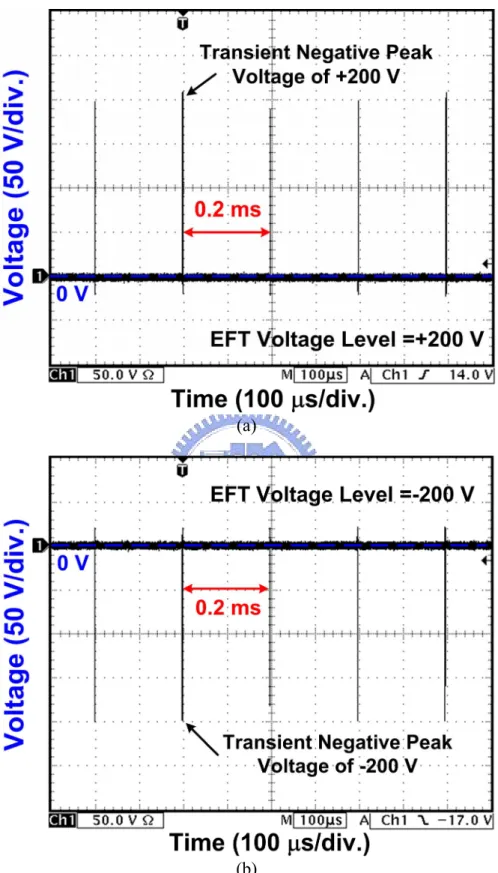
For EFT pulses with the repetition frequency of 5 kHz, the measured +200-V and -200-V voltage waveforms on the 1-kΩ load are shown in Figs. 1.8(a) and 1.8(b), respectively. Because the output loading (1 kΩ) is larger than the impedance matching resistor Rm (50 Ω),
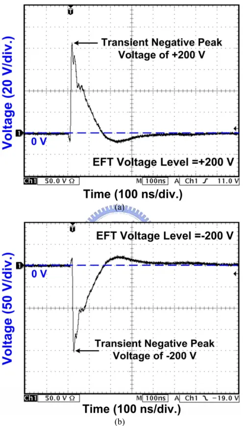
the measured output pulse peak is close to the input EFT voltage pulse. As shown in Figs. 1.8(a) and 1.8(b), the measured output pulse peaks on the 1-kΩ load are approximately +200 V and -200 V, respectively. For EFT repetition frequency of 5 kHz, the time interval between each pulse is 0.2ms. Under EFT tests, the application time should not be less than 1 minute and both polarities have to be tested. With the 1 kΩ load, the voltage waveforms of a single pulse with EFT voltage of +200 V and -200 V are shown in Figs. 1.9(a) and 1.9(b), respectively. In Figs. 1.9(a) and 1.9(b), the waveforms of a single pulse have a rise time of ∼5ns and the pulse duration (time interval at half of peak EFT voltage) of ∼50 ns. The characteristics of a single EFT pulse are summarized in Table 1.7.
Table 1.6
Characteristics of the Fast Transient/Burst
Table 1.7
(a)
(b)
Fig. 1.8 Measured voltage waveforms under EFT tests with EFT voltage of (a) +200 V, and (b) -200 V, on 1-kΩ load with a repetition rate of 5 kHz.
(a)
(b)
Fig. 1.9 Measured voltage waveforms of a single pulse with EFT voltage of (a) +200 V, and (b) -200 V, on 1-kΩ load under EFT test.
The EFT levels for testing power supply ports and for testing I/O, data, and control ports of the equipment are listed in Table 1.8. The voltage peak for testing I/O, data, and control ports is half of the voltage peak for testing power supply ports. The repetition rate is determined by specific products or product types. Level “X” is an open level, which is specified in the dedicated equipment specification by customers. The output voltage peaks of EFT test are listed in Table 1.9. With output load of 50 Ω, the measured output voltage is 0.5 times the value of open-circuit load due to impedance matching.
Table 1.8 Levels of EFT Test
Table 1.9
1.3. Solutions to Overcome Electrical Transient Disturbance
1.3.1. Traditional Board-Level Solution
In order to meet the system-level ESD specifications, two useful methods have been reported and investigated [30]-[34]. One effective method is to add some discrete noise-bypassing components or board-level noise filters into the CMOS IC products to decouple, bypass, or absorb the electrical transient voltage (energy) under system-level ESD test. The system-level ESD immunity of CMOS ICs under system-level ESD test can be significantly enhanced by choosing proper noise filter networks. As shown in Fig. 1.10, some discrete components (such as the magnetic core, ferrite bead (FB), and RC low-pass filters) are added into printed circuit board (PCB) of a keyboard product to restrain the electrical transients from the system-level ESD tests. The system-level ESD immunity of CMOS ICs under system-level ESD test can be significantly enhanced by choosing proper noise filter networks. The other method to improve the system-level ESD immunity of CMOS ICs is to regularly check the system abnormal conditions by using an external hardware timer, such as watch dog timer. The external hardware timer is often consisted of registers or flip flops to reset the operation system if the main program is locked or frozen due to some fault conditions. However, during system-level ESD tests, the logic states stored in the registers or flip flops may be destroyed or changed to cause malfunction or frozen state on the main operation program. The additional discrete noise-bypassing components also substantially increase the total cost of microelectronic products. Therefore, the chip-level solutions to meet high transient disturbance immunity specification for microelectronic products without additional discrete noise-decoupling components are highly desired by IC industry [35]-[39].
Fig. 1.10 A traditional solution to overcome the electrical transient disturbance in a keyboard product by adding extra discrete components to absorb or bypass the electrical transients.
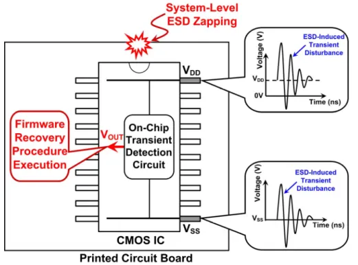
1.3.2. Hardware/Firmware System Co-Design Solution
It had been reported that the hardware/firmware co-design can effectively improve the system-level ESD susceptibility of the CMOS IC products [10]. In this work, a new on-chip transient detection circuit is proposed to detect the fast electrical transient under system-level ESD or EFT tests. By using a longer time delay in the RC circuit under system-level ESD tests, the proposed new on-chip transient detection circuit can memorize the occurrence of electrical transient disturbance events. As shown in the hardware/firmware system co-design in the Fig. 1.11, the detection results (VOUT) from the proposed on-chip transient detection
circuit can be temporarily stored as a system recovery index for firmware check.
Fig. 1.11. Hardware/firmware co-design for system recovery by using the output of the on-chip transient detection circuit.
For example, the output (VOUT) states in the proposed on-chip transient detection circuit
and the firmware index are initially cleared to logic “0.” When the fast electrical transient happens, the proposed on-chip transient detection circuit can detect the fast electrical transients to transit the output state (VOUT) from logic “0” to logic “1.” At this time, the
system recovery index is stored at logic “1” and the firmware executes the recovery procedure to recover all system functions to a stable state as soon as possible. After the recovery procedures, the output state of the proposed on-chip transient detection circuit and the firmware index are re-set to logic “0” again for detecting the next system-level ESD events. A novel on-chip transient-to-digital converter composed of transient detection circuits
was proposed to detect the fast electrical transients and convert them to digital thermometer codes under system-level ESD or EFT tests. The proposed on-chip transient-to-digital converter can be also coordinated with firmware to provide a hardware/firmware co-design solution for protection design against electrical transient disturbance.
1.4. Organization of This Dissertation
This dissertation is composed of seven chapters. This dissertation (chapter 2 ~ chapter 6) focuses on the system-level ESD issues and the design of on-chip transient detection circuits and transient-to-digital converter. Several major topics including: (1) investigation and design of on-chip power-rail ESD clamp circuits without suffering latchup-like failure during system-level ESD and EFT tests (chapter 2), (2) transient-induced latchup in CMOS integrated circuits under EFT tests (chapter 3), (3) on-chip transient detection circuit design (scheme I) (chapter 4), (4) on-chip transient detection circuit design (scheme I) (chapter 5) , and (5) transient-to-digital converters (chapter 6). Chapter 7 gives the conclusions and future works of this dissertation. The outlines of each chapter are summarized below.
In chapter 2, on-chip power-rail electrostatic discharge (ESD) protection circuit designed with active ESD detection function is the key role to significantly improve ESD robustness of CMOS ICs. Four power-rail ESD clamp circuits with different ESD-transient detection circuits were fabricated in a 0.18-μm CMOS process and tested to compare their system-level ESD and EFT susceptibility, which are named as power-rail ESD clamp circuits with typical RC-based detection, PMOS feedback, NMOS+PMOS feedback, and cascaded PMOS feedback in this work. During the system-level ESD and EFT tests, where the ICs in a system have been powered up, the feedback loop used in the power-rail ESD clamp circuits provides the lock function to keep the ESD-clamping NMOS in a “latch-on” state. The latch-on ESD-clamping NMOS, which is often drawn with a larger device dimension to sustain high ESD and EFT testing levels, conducts a huge current between the power lines to perform a latchup-like failure after the system-level ESD and EFT tests. A modified power-rail ESD clamp circuit is proposed to solve this problem. The proposed power-rail ESD clamp circuit can provide high enough chip-level ESD robustness, and without suffering the latchup-like failure during the system-level ESD and EFT tests.
In chapter 3, the occurrence of transient-induced latchup (TLU) in CMOS ICs under the EFT tests is studied. The test chip with the parasitic silicon-controlled rectifier (SCR) structure fabricated by a 0.18-μm CMOS process was used in the EFT tests. For physical
mechanism characterization, the specific “sweep-back” current caused by the minority carriers stored within the parasitic PNPN structure of CMOS ICs is the major cause of TLU under EFT tests. Different types of board-level noise filter networks are evaluated to find their effectiveness for improving the immunity of CMOS ICs against TLU under EFT tests. By choosing proper components in each noise filter network, the TLU immunity of CMOS ICs against EFT tests can be greatly improved.
In chapter 4, a novel on-chip RC-based transient detection circuits for system-level ESD)and EFT protection are proposed in this work. The circuit performance to detect positive and negative electrical transients under system-level ESD and EFT testing conditions has been investigated by the HSPICE simulation and verified in silicon chip. The experimental results have confirmed that the proposed on-chip RC-based transient detection circuit I can successfully memorize the occurrence of the system-level ESD and EFT events. The detection output of proposed on-chip RC-based transient detection circuit I can be used as the firmware index to execute system recovery procedure to provide a hardware/firmware co-design to improve the immunity of CMOS IC products against electrical transient disturbance.
In chapter 5, a new on-chip transient detection circuit II for electrical fast disturbance protection design is proposed in this work. The circuit performance to detect different positive and negative ESD-induced or EFT-induced transient disturbance has been investigated by the HSPICE simulation and verified in silicon chip. The EFT generator combined with attenuation network and capacitive coupling clamp has been used as the evaluation method to verify the detection function of the proposed on-chip transient detection circuit II under EFT tests. The test chip in a 0.18-μm CMOS process with 1.8-V devices has confirmed that the proposed on-chip transient detection circuit II can successfully detect and memorize the occurrence of the transient disturbance under system-level ESD or EFT tests.
In chapter 6, a novel on-chip transient-to-digital converter composed of four RC-based transient detection circuits and four different RC filter networks has been successfully designed and verified in a 0.18-μm CMOS process with 3.3-V devices. The output digital thermometer codes of the proposed on-chip transient-to-digital converter correspond to different electrical transient voltages under system-level ESD and EFT tests. These output digital codes can be used as the firmware index to execute different auto-recovery procedures in microelectronic systems. Thus, the proposed on-chip transient-to-digital converter can be further combined with firmware design to provide an effective solution to solve the
system-level ESD and EFT protection issue in microelectronic systems equipped with CMOS ICs.
Chapter 7 summarizes the main results of this dissertation. Some suggestions for the future works are also addressed in this chapter.
Chapter 2
Investigation and Design of On-Chip Power-Rail
ESD Clamp Circuits Without Suffering
Latchup-Like Failure During System-Level ESD and
EFT Tests
On-chip power-rail electrostatic discharge (ESD) protection circuit designed with active ESD detection function is the key role to significantly improve ESD robustness of CMOS integrated circuits (ICs). Four power-rail ESD clamp circuits with different ESD-transient detection circuits were fabricated in a 0.18-μm CMOS process and tested to compare their system-level ESD susceptibility, which are named as power-rail ESD clamp circuits with typical RC-based detection, PMOS feedback, NMOS+PMOS feedback, and cascaded PMOS feedback in this work. During the system-level ESD and EFT tests, where the ICs in a system have been powered up, the feedback loop used in the power-rail ESD clamp circuits provides the lock function to keep the ESD-clamping NMOS in a “latch-on” state. The latch-on ESD-clamping NMOS, which is often drawn with a larger device dimension to sustain high ESD level, conducts a huge current between the power lines to perform a latchup-like failure after the system-level ESD test. A modified power-rail ESD clamp circuit is proposed to resolve this problem. The proposed power-rail ESD clamp circuit can provide high enough chip-level ESD robustness, and without suffering the latchup-like failure during the system-level ESD and EFT tests.
2.1. Background
ESD protection has been one of the most important reliability issues in CMOS IC products. ESD failures caused by thermal breakdown due to high current transient, or dielectric breakdown in gate oxide due to high voltage overstress, often result in immediate malfunction of IC chips. In order to obtain high ESD robustness, CMOS ICs must be designed with on-chip ESD protection circuits at the input/output (I/O) pins and across the power lines. With the reduced breakdown voltage of the thinner gate oxide in advanced deep-submicron CMOS processes, turn-on-efficient ESD protection circuit is required to