國
立
交
通
大
學
電子工程學系 電子研究所
博 士 論 文
介面保護與雷射退火增進高效能 N 型鍺電晶體之研究
The Research of High Performance Ge nMOSFET
Improved by Interface Passivation and Laser Annealing
研 究 生:陳維邦
指導教授:荊鳳德 教授
介面保護與雷射退火增進高效能 N 型鍺電晶體之研究
The Research of High Performance Ge nMOSFET Improved by Interface
Passivation and Laser Annealing
研 究 生:陳維邦 Student:Wei-Barn Chen
指導教授:荊鳳德 Advisor:Albert Chin
國 立 交 通 大 學
電子工程學系 電子研究所
博 士 論 文
A DissertationSubmitted to Department of Electronics Engineering and Institute of Electronics
College of Electrical and Computer Engineering National Chiao Tung University
in partial Fulfillment of the Requirements for the Degree of
Doctor of Philosophy in
Electronics Engineering
Oct. 2010
Hsinchu, Taiwan, Republic of China
介面保護與雷射退火增進高效能 N 型鍺電晶體之研究
研究生:陳維邦 指導教授:荊鳳德教授
國立交通大學
電子工程學系 電子研究所
摘要
隨著半導體元件尺寸的不斷縮微,並且符合目前邏輯電路與高效能場效電晶 體的發展,高效能的金氧半互補式場效電晶體 (CMOSFET) 的研發是勢在必行 的。當以矽 (Si) 為基板與二氧化矽(SiO2) 為介電材料的半導體元件發展到一 個瓶頸時,為了符合未來尺寸的微縮與高效能電晶體與的趨勢,高介電系數材料 與高載子遷移率材料的開發似乎是不二法門。但增加介電常數和減少元件厚度所 伴隨而來的高漏電與如何整合這些高介電材料在新基板更是目前研究的主要議 題。而目前許多高介電材料如 HfO2、 Al2O3、 La2O3、 TiO2等都被廣泛的研究。除此之外,一些高電子遷移率的基板,如矽鍺 (SiGe)、鍺 (Ge) 與砷化鎵 (GaAs)
等,再近幾年也都陸陸續續被提出一些相關的研究文件,然而如何成功的整合這 些新材料與新基板應用於大型積體電路上依然是一個困難的課題。 因此,我們針對新材料與基板所產生的問題,開發出一系列和氧化鑭相關 (La2O3-based)的高介電材料,其中包括了鑭化鋁氧化物(LaAlO3)、鑭化鈦氧化物 (TiLaO) 和 二氧 化鋯 (ZrO2) 。 除 此 之 外 ,我們 也 成 功 的 研 究出 整合 介 面 工 程 (Interface engineering) 與高介電材料的方法,成功的運用在鍺基板與高介電材料
之間沈積一層很薄的二氧化矽保護層來做出高性能的 N 型鍺互補式金氧半場效 電晶體 (Ge nMOSFET),不但在漏電上有大幅的降低,更改善了鍺基板介面的一 些平帶電壓(Flatband Voltage)的不理想效應,大大的增進了電容密度,使等效氧 化曾厚度(EOT)在鍺基板可以微縮到 0.85 奈米 並且得到了高的電子遷移率。 最後,由於前面成功的實驗,我們再加以運用雷射退火(Laser Annealing)的方式, 使電晶體的特性更進一步的改善。
The Research of High Performance Ge nMOSFET
Improved by Interface Passivation and Laser
Annealing
Student:Wei-Barn Chen Advisor: Albert Chin
Department of Electronics Engineering & Institute of
Electronics National Chiao Tung University
Abstract
The development of the high performance complementally
metal-oxide-semiconductor field effect transistors (CMOSFET) is expected to be
imperative as the semiconductor devices continuously decrease in size along with the
development of current logical circuits and high performance MOSFET. However, the
size reduction of the Si-substrate and silicon dioxide (SiO2)-dielectric-material-based
semiconductor devices has come to a bottleneck due to their low carrier mobility and
the lower dielectric permittivity constants (=3.9), hence the development of
materials with higher dielectric constant materials and higher carrier mobility is
unavoidable.
The high leakage currents accompanying the reduction of the thickness of the
devices and the increase in the dielectric constants, and the integration of these high
the recent studies. The researches of high dielectric constant materials, such as HfO2,
Al2O3, La2O3, and TiO2 have been studied for decades. Furthermore, high carrier
mobility substrates, such as SiGe, Ge, and III-V compounds (GaAs), have been
widely proposed in some recent research articles. Nevertheless, successful integration
of high dielectric constant materials onto new substrates for the VLSI technology still
proves to be quite a difficult issue.
In order to overcome the problems of integrating the new high dielectric constant
materials and the substrates, we used a series of Lanthanum Oxide (La2O3)-based
high- materials such as LaAlO3, TiLaO and ZrO2. We had also studied the interface
engineering and successfully fabricated high performance Ge nMOSFET by
depositing an ultra thin SiO2 passivation layer between the Ge substrates and the high
dielectric materials. Using the interface passivation not only reduces the electric
leakages, but also improves the unwanted flat-band voltage (Vfb) shifts on the Ge
substrates as well as the capacitance density, enabling the equivalent oxide thickness
(EOT) to scale down to 0.85 nm with higher carrier mobility. Finally, we used the
laser annealing (LA) method to further improve the transistor characteristics of the
Acknowledgements
首先我要感謝我的指導教授荊鳳德教授,我才能順利的完成此博士論文。 在荊教授耐心的教導之下,學到了許多實驗的研究方法,遇到問題學會去思考並 且尋求解決之道,以及待人處世應有的腳踏實地與務實的態度,讓我博士班生涯 受益良多。 再來我要感謝淳護、迺超和明峰等學長的指導和思麟同學的相互鼓勵,還有 竣揚、坤億、博璿、柏君、智偉、阿爆、和佳芸各位學弟妹在實驗上熱情的幫忙 與給我意見,讓我可以更有信心並且順利的完成我的實驗。由於也因有為你們這 群好學長、好同學與好學弟妹讓我4年的碩博士班生涯過的很充實也很有意義, 也希望你們未來的實驗都很順利。同時也感謝Joyce Chiang英文撰寫的幫忙。 我也由衷感謝交通大學奈米中心與國家實驗研究院-國家奈米元件實驗室, 能讓我有完善的儀器設備與環境來達成我的實驗。 最後我要對我親愛的父母親以及大姊莉玲,大哥維新以及盈燕一路無悔的支 持我念完博士班致上最高的感謝,並且支持我所做的一切,讓我可以全心全力無 後顧之憂的朝自己的夢想努力與邁進。Contents
Abstract (Chinese)……….……….……….………i
Abstract (English) ………..……….……….………….…iii
Acknowledgement……….……….……….………v
Contents……….……….………….……vi
Table Captions……….……….……….…ix
Figure Captions……….……….……….……x
Chapter 1 Introduction
1.1
Motivation of High- Dielectrics………...……….11.2
Overview of Metal Electrode...………...……….61.3
The Challenge of Ge n-type MOSFETs…………...…………...71.4
Dissertation Organization ………...………10 Chapter 2 High Performance Gate-First Epitaxial Ge n-MOSFETs on Si with LaAlO3 Gate Dielectrics
2.1
Introduction………..…….………142.2
Experimental Procedure………..………...…………152.3
Results and Discussion…………..……….…………162.4
Conclusion………..……….…..……21TiLaO Ge/Si N-Type Metal-Oxide-Semiconductor Capacitors at Small
Equivalent-Oxide Thickness
3.1
Introduction………….………..………..…293.2
Experimental Procedure………..………..…303.3
Results and Discussion………..………...………..………313.4
Conclusion………..……….…..……33 Chapter 4 High Performance of Ge n-MOSFETs Using SiO2 Interfacial Layer and TiLaO Gate Dielectric
4.1
Introduction………..………...………..……394.2
Experimental Procedure……….…………..………..………404.3
Results and Discussion………..………414.4
Conclusion………...………..…42 Chapter 5 High Field Mobility Metal-Gate/high-κ Ge n-MOSFETs with Small Equivalent-Oxide-Thickness
5.1
Introduction………..………...………..……485.2
Experimental……….…………..………..……495.3
Results and Discussion………..………505.4
Conclusion……….……….………..… 54Annealing
6.1
Introduction………..….………626.2
Experimental Procedure………..………...…………636.3
Results and Discussion…………..……….…………646.4
Conclusion………..……….…..……66 Chapter 7 Higher Gate Capacitance Ge n-MOSFETs Using Laser Annealing
7.1
Introduction………..….……….……727.2
Experimental Procedure...737.3
Results and Discussion...747.4
Conclusion...76 Chapter 8 Conclusions………….……….……….81
References……….………83
Vita……….………109
Table Captions:
Chapter 1 Introduction
Table 1-1. Comparisons of Si, Ge and GaAs [1-19]...13
Chapter 2 High Performance Gate-First Epitaxial Ge n-MOSFETs
on Si with LaAlO
3Gate Dielectrics
Table 2-1. Comparison of device integrity data for various metal-gate/high-κ Ge
n-MOSFETs...22
Chapter 5 High Field Mobility Metal-Gate/high-
Ge n-MOSFETs
with Small Equivalent-Oxide-Thickness
Table 5-1. Comparison of device integrity data for various metal-gate/high-κ Ge
n-MOSFETs...55
Chapter 6 Gate-First TaN/La
2O
3/SiO
2/Ge n-MOSFETs Using Laser
Annealing
Table 6-1. Comparison of device data of various metal -gate/high-κ/Ge
Figure Captions:
Chapter 1 Introduction
Fig. 1.1 Leakage current versus voltage for various thicknesses of SiO2 layers...11
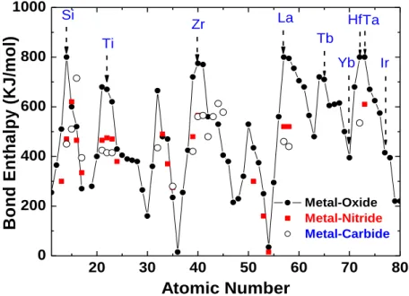
Fig. 1.2 International Technology Roadmap for Semiconductor (ITRS), [Online] Available: http://public.itrs.nrt/...11 Fig. 1.3 Static dielectric constant versus band gap for candidate gate oxides [1-10]. Fig. 1.4 The band offset of popular high- materials...12 Fig. 1.5 Bond enthalpy for M-O, M-N and M-C in the Periodic Table...13
Chapter 2 High Performance Gate-First Epitaxial Ge n-MOSFETs
on Si with LaAlO
3Gate Dielectrics
Fig. 2.1 C-V characteristics of (a) TaN/HfAlO/Ge/Si and control TaN/HfAlO/Si n-MOS capacitors and (b) TaN/LaAlO3/Ge/Si n-MOS capacitors at 100 kHz
after 450~550oC RTA...23 Fig. 2.2 (a) J-V characteristics of TaN/LaAlO3/Ge/Si and TaN/HfAlO/Ge/Si n-MOS
capacitors after 450oC~550oC RTA. (b) J-EOT characteristics of TaN/LaAlO3/Ge/Si n-MOS capacitors after550oC RTA...24
Fig. 2.3 Cross-sectional TEM of (a) TaN/HfAlO/Ge/Si capacitor, (b) control TaN/HfAlO/Si and (c) TaN/LaAlO3/Ge/Si capacitors after 550oC RTA...25
Fig. 2.4 (a) Id-Vd and (b) Id-Vg characteristics of gate-first TaN/LaAlO3/Ge/Si
n-MOSFETs after 550oC RTA. The gate length and width are 10 and 100 m, respectively...26 Fig. 2.5 Electron mobility vs. effective electric field of TaN/LaAlO3/Ge/Si
n-MOSFET and other published data for comparison……...27
Chapter 3 Interfacial Layer Dependence on Device Property of
High-
TiLaO Ge/Si N-Type Metal-Oxide-Semiconductor
Capacitors at Small Equivalent -Oxide Thickness
Fig. 3.1. C-V characteristics of TaN/TiLaO Ge/Si n-MOS capacitors with or withoutthe inserted GeO2 and SiO2 interfacial layer and after 450 or 550oC RTA.
The device size is 100-mx100-m...35 Fig.3.2. Cross-sectional TEM images of TaN/TiLaO/GeO2/Ge/Si n-MOS capacitors
(a) before and (b) after 550oC RTA. (c) TaN/TiLaO/SiO2/Ge/Si n-MOS
capacitors after 550oC RTA...36 Fig. 3.3. SIMS profile of TaN/TiLaO Ge/Si n-MOS structure with inserted (a) GeO2
and (b) SiO2 interfacial layer before and after 550oC RTA...37
Fig. 3.4. The Ge 2p3 XPS spectra of TiLaO/GeO2/Ge/Si structure before and after
550oC RTA...38
Chapter 4 High Performance of Ge n-MOSFETs Using SiO
2Layer
and TiLaO
Gate Dielectric
Fig. 4.1. C-V and of the TaN/TiLaO on Si-Capped Ge/Si n-MOS capacitors after 450~550oC RTA...44 Fig. 4.2. (a) The C-V and (b) J-V characteristics of the TaN/TiLaO/SiO2 on Ge/Si
n-MOSFETs 450~550oC RTA. The inserted figure in (b) is the J-CET plot at 1 V above Vfb...45
Fig. 4.3. (a) The Id-Vd and (b) Id-Vg characteristics of the TaN/TiLaO/SiO2 on Ge/Si
n-MOSFETs...46
Fig.4. 4. The electron mobility as a function of effective electric field for the TaN/TiLaO/SiO2 on Ge/Si n-MOSFETs...47
with Small Equivalent-Oxide-Thickness
Fig. 5.1 (a) Schematic image of TaN/La2O3/SiO2/Ge n-MOSFET and (b) process
flow of gate-last Ge-n MOSFET...56 Fig. 5.2. (a) C-V and (b) J-V characteristics of TaN/La2O3/SiO2/Ge n-MOS capacitors
with different PDA temperatures...57 Fig. 5.3. (a) SIMS depth profile of TaN/La2O3/SiO2/Ge at a 400oC PDA. (b)
Cross-sectional TEM of TaN/La2O3/SiO2/Ge after a 400oC PDA...58
Fig. 5.4. (a) Id-Vd and (b) Id-Vg plots of TaN/La2O3/SiO2/Ge n-MOSFET...59
Fig. 5.5. The electron mobility as a function of effective electric field of TaN/La2O3/SiO2/Ge n-MOSFETs...60
Fig. 5.6. The comparison of electron peak mobility of Ge n-MOSFETs...61
Chapter 6 Gate-First TaN/La
2O
3/SiO
2/Ge n-MOSFETs Using Laser
Annealing
Fig. 6.1. (a) Sheet resistance and (b) n+/p junction characteristics of As+-implanted Ge after laser annealing...68 Fig. 6.2. (a) C-V and (b) J-V characteristics of TaN/La2O3/SiO2/Ge n-MOS capacitors
before and after laser annealing. The insert figure is the cross-sectional TEM after laser annealing...69 Fig. 6.3. (a) Id-Vd and (b) Id-Vg of gate-first TaN/La2O3/SiO2/Ge n-MOSFET using
laser annealing...70 Fig. 6.4. The electron mobility as a function of effective electric field of
TaN/La2O3/SiO2/Ge n-MOSFETs using laser annealing...71
Chapter 7 Higher Gate Capacitance Ge n-MOSFETs Using Laser
Annealing
TEM after LA...77 Fig. 7.2. The n+/p junction characteristics of P+-implanted Ge after LA...78 Fig. 7.3. (a) Id-Vd and (b) Id-Vg of TaN/ZrO2/La2O3/SiO2/Ge n-MOSFET using LA...79
Fig. 7.4. The electron mobility as a function of effective electric field of TaN/ZrO2/La2O3/SiO2/Ge n-MOSFET using LA...80
Chapter 1
Introduction
1.1. Motivation of High-
Dielectrics
The scaling down of Metal-Oxide-Semiconductor Field Effect Transistor
(MOSFETs) using metal gate with high has been the major way to improve the
performance of integrated circuits in the last few decades. Si dioxide (SiO2) as a gate
dielectric offers some merits in CMOS processing including a thermodynamically and
electrically stable, high-quality Si–SiO2 interface as well as superior electrical
isolation properties. In order to scale down the MOSFETs, reducing the thickness of
gate dielectric becomes the trend for the state-of-the-art devices. However, the direct
tunneling of gate leakage at 2V bias exceeds 1A/cm2 below the 2.0 nm thickness of
SiO2 (Fig.1-1) which becomes the critical issue for CMOS scaling down [1-1].
From the below electrical fundamental equation, we can solve the obstacle by
using the materials with high dielectric constant (high-):
(1) Where (8.85x10⁻¹⁴ f/cm2) is the permittivity of free space, is the dielectric constant (also referred to relative permittivity in this article), A is the area of capacitor,
be increased without the reduction of capacitance density if using the higher dielectric
constant material. Higher C value enables the MOS structure to gain more inversion
carriers and reaches the higher drive current of MOSFETs. In the other hand to
increase the C, we can reduce the overall t thickness. The components of t can be
represented as the following equation,
t = t
qm+ t
ox+ t
poly-si(2)
where tpoly-si is from the poly-Si depletion, tox is the equivalent oxide thickness
(EOT) of the dielectric and tqm is the quantum effect of carriers in the channel. tqm is
the intrinsic physic quantum effect and is not avoidable. We can reduce tox and tpoly-Si
to increase the capacitance density. Using metal gates to replace the poly-Si gate have
been proposed to solve the issue in recent years. Reducing the EOT becomes the most
important way to reach higher C. The EOT of materials is defined as the thickness of
SiO2 required to reach the same capacitance. EOT can be written as an equation,
(3) where thigh-dielectric and high-dielectric are the high material of physical thickness and
relative dielectric constant, respectively.
According to the ITRS (International Technology Roadmap for Semiconductor)
shown in Fig. 1.2, the EOT for metal gate has to be below 10 Å after 2010. Therefore,
technology.
Although a lot of researches of high dielectric constant materials have been
reported, we still need to understand before these materials can be adopted by industry.
There are some key points listing below [1-2].
Permittivity
The relative dielectric constant of the new material should be between 10 and 30.
Higher dielectric materials will give rise to fringe fields from the gate to the
drain or source and it will degrade the short channel device performance.
Band gap
The band gap of new dielectric materials must be greater than 5 eV and the band
offsets with silicon must be sufficient. Generally, Fig. 1.3 shows the higher
value materials will have a smaller band gap, and there is an inverse relationship
between band gap and dielectric constant. Fig.1.4 shows that increasing
dielectric constant will cause lower conduction band and valence band when in
contact with silicon. In order to reduce the leakage current from each band, the
barrier height must be bigger than 1 eV.
Thermodynamic stability
Good thermodynamic stability is required for new high dielectric materials to
High- dielectric materials must have a large Gibbs free energy to prevent
interaction with silicon, and the diffusion coefficient of materials must be low
with less interface reaction.
Interface quality
The interface between high dielectric material and silicon is also an important
issue. Interface states will cause flat-band voltage shift and degrade the mobility
of MOSFETs. Low interface trap defect density, Dit, should be lower than 1011
cm-1 eV-1.
Compatibility with the current or expected materials to be used for CMOS
devices
Therefore, alternate high dielectric materials such as Si3N4 (= 7.5), SixOyNz
(= 3.9-7.5), Al2O3 (= 10), HfO2 (= 26), La2O3 (= 30), Ta2O5 (= 25), TiO2 (=
50), and ZrO2 (= 25) [1-3]-[1-8], or other dopant metal oxides have been proposed
to replace SiO2 for gate dielectric materials in the recent researches. Fig. 1-5 shows
the bond enthalpies for various metal/dielectric combinations. High dielectric constant
materials have higher bond enthalpies, which can prevent higher leakage currents and
degradations after high temperature processes. In general, the metal oxides exhibit
strong bond enthalpies than other compounds.
CMOS devices. Such as, Al2O3,is not thermodynamically stable in direct contact with
Si with a lower dielectric constant and Ta2O5 has a smaller conduction band offset
with silicon (c~0.3 eV) that will cause the increasing leakage currents from
electron tunneling.
In this study, we used different high k dielectric LaAlO3 (LAO) and TiLaO for
gate dielectrics for comparisons. As we know, La2O3 has a high k value (k ~30) and
the negative flat-band voltage for nMOSFETs [1-9]. However, La2O3 easily absorbed
water vapor from air and results in an uncontrolled reaction [1-10]. Moreover, the
band gap of La2O3 is relatively small (4.3 eV) and the structure transition from the
amorphous to crystalline phase occurs at a lower temperature than that of Al2O3 [1-11]
which induces large leakage current from the grain boundary after high thermal
budget. Lanthanum aluminate LaAlO3 (LAO), as a compound of La2O3 and Al2O3,
has a reasonably larger value of 25, band-gap of over 5 eV, high thermal stability up
to 2100oC. It presents the chemical and dielectric properties of La2O3 and Al2O3 and
overcome the obstacles of individual materials [1-12]-[1-14].
On other hand, although TiO2 has a high dielectric constant value of 86, it is
easily to form anatase phase at the temperature of 400oC with high leakage current
and low bandgap (3.5 eV) for amorphous film [1-15]. Besides, the smaller conduction
the La2O3 dopant into TiO2 with a value of 45 and maintains the high permittivity
constant of TiO2 and negative flat-band voltage from La2O3 [1-16]. We will focus on
the Lanthanum (La) based high dielectric for advanced gate stacks application with
alternative channel material in this thesis.
1.2. Overview of Metal Gate Electrode
As complementally metal oxide semiconductor field effect transistors
(CMOSFETs) scaling down to 100 nm technology node or beyond, the conventional
poly-Si gate electrode has concerned due to following issues [1-17]:
Poly-Si depletion effects.
Boron penetration effects.
High sheet resistance.
An obvious way to alleviate the problems of poly-Si is to use metal or metal
nitride gates. The requirement of the new technology metal gates should suit for the
follows:
Favorable work functions (Φm) [candidate metals need to have vacuum
work-functions smaller (larger) than 4.05 V (5.17 V) for the NMOS (PMOS)]
[1-16].
Low sheet resistance.
Compatibility with high- dielectric and integration with VLSI technology.
In selecting metal-gate materials for device integration, the metal work function
(Φm) is an important consideration since it directly affects the threshold voltage and
the performance of a transistor. Using TaN for gate electrode has been widely
studied for recently years. It shows promising results as gate electrodes for high-
gate dielectrics in terms of thermal stability and compatibility with the high-k gate
dielectrics. Besides, there is a significant variance in reported work-function from
4.13 eV (close to n+ poly-Si) to 5.05 ev (close to p+ poly-Si) [1-17]-[1-18]. Causing
these large discrepancies are due to different deposition methods, different nitrogen
ratios and post metal deposition annealing (PMA). In this article, we used the TaN
for integration of metal gates / high-to study the characteristics of MOSFETs.
1.3. The Challenge of Ge n-type MOSFETs
As we knew, carrier mobility is an important issue for high performance devices.
Many studies of strained-Si had been proposed to enhance the mobility of devices.
Germanium as channel is attractive because of its significant enhancement in bulk
mobility relative to Si. It can enhance the electron mobility (2X) and hole mobilities
(4X) higher than Si. Besides, the Ge has ~50X higher density of state than InGaAs to
deliver high transistor current. Although the III-V compounds show the higher
obstacles which degrade the MOSFET performance and cannot meet the trend for
ITRS. The comparisons of Si, Ge and GaAs are listed in the Table 1 [1-19]. Therefore,
several successful demonstrations of high materials gate stacks on Ge have been
reported recently [1-20]-[1-25]. However, there are still some problems on Ge
substrates for the MOSFET fabrication needed to be solved and listed below [1-25]:
(a) Germanium oxide (GeOx x < 2) is thermal unstable and water soluble.
(b) Large off state leakage currents due to small bandgap (0.66 eV).
(c) The poor interface between Ge and high- dielectric materials.
(d) Activation is insufficient for source/drain and the low contact resistivity is hard to
form for Ge nMOSFETs.
Therefore, reduction of interface reaction between Ge and high- dielectric
material to form GeOx is becoming a critical issue. There are some reports
demonstrate the Ge surface passivation to suppress the unstable GeOx formation
during high- deposition. Surface nitridation using NH3 for Ge passivating had been
studied [1-26]. However, the nitrogen involvement caused the degradation of mobility.
Using a thin Si passivation layer on Ge also had been proposed to solve the interface
states [1-27]. Unfortunately, the Si layer is not easily to control during the process
thermal budget and causes the equivalent oxide thickness (EOT) degradation. Using
are also alternative ways for the solution [1-28]-[1-29]. Such reports have been
successfully proposed the high performance devices and show the high low-field
mobilities. However, the degradation of EOT is still the issue for Ge technology. As
mention above, another obstacle for Ge MOSFET is about the dopant activation of
source/drain junction. As we knew, the boron activation using conventional rapid
thermal annealing (RTA) is at a low 400oC temperature. However, the higher activation temperature is needed ( 600o
C) for phosphorus or arsenic [1-30]. Such
high temperature not only caused the unwanted interface reaction but also degrade the
device performance. Besides, the insufficient n type dopant activation by using RTA
had also been reported [1-31]. Furthermore, the diffusion coefficient for the n-type
dopant (phosphorus or arsenic) is faster than the p-type dopant (boron) [1-30].
Therefore, it is hard for n type dopants to form the shallow junction with a low sheet
resistance by RTA [1-31]. In order to increase the efficiency of dopant activation, the
method of using Excimer laser annealing (LA) had been demonstrated successfully to
enhance the source/drain complete activation [1-32]-[1-33]. We had demonstrated the
LA for S/D junction activation. Furthermore, the LA also was applied for increasing
the value for gate stacks due to crystallization-induced.
1.4. Dissertation Organization
In chapter 2, we discussed the n MOSFET for depositing the high-dielectric
LaAlO3 for the gate material without passivation layer on Ge channel. Although it was
successful for surface passivation for Ge channel MOSFET, the EOT degraded.
In order to further scale down the EOT for Ge channel MOSFET, we used the
TiLaO higher material and SiO2 interfaciallayer for surface passivation. These not
only improved the interface but also reached the same mobility. Therefore, we
discussed the effect of SiO2 passivation layer and less flat-band (Vfb) shift in chapter 3
and the performance of Ge n channel MOSFET in chapter 4.
However, the mobility was still not high for strained-Ge. In chapter 5 and chapter
6, we used the La2O3 with SiO2 for gate stacks on Ge substrate by conventional RTA
and laser annealing (LA) for source and drain activation.
Finally, we used the ZrO2/La2O3/SiO2 on Ge substrate for further EOT scaling
down by LA in chapter 7. The LA was applied on gate stacks for increasing the
capacitance density due to the crystallization-induced and the efficient activation for
source/drain.
Fig. 1.1 Leakage current versus voltage for various thicknesses of SiO2 layers.
Fig. 1.2 International Technology Roadmap for Semiconductor (ITRS), [Online]
Fig. 1.3 Static dielectric constant versus band gap for candidate gate oxides [1-34].
Fig. 1.5 Bond enthalpy for M-O, M-N and M-C in the Periodic Table.
Si Ge GaAs
Dielectric constant () 11.9 16 13.1
Band gap (eV) 1.12 0.66 1.42
Hole mobility (cm2/Vs) 480 1900 400 Electron mobility(cm2/Vs) 1350 3900 8500 Density of states in valence band (cm-3) 1.04 x 10¹⁹ 6.0 x 10¹⁸ 7.0 x 10¹⁸ Density of states in conduction band (cm-3) 2.8 x 10¹⁹ 1.04 x 10¹⁹ 4.7 x 10¹⁷ 20 30 40 50 60 70 80 0 200 400 600 800 1000 Metal-Oxide Metal-Nitride Metal-Carbide B o n d E n th a lp y ( K J /m o l) Atomic Number Ti Ta Hf La Yb Tb Ir Zr Si
Chapter 2
High Performance Gate-First Epitaxial Ge
n-MOSFETs on Si with LaAlO
3Gate Dielectrics
2.1. Introduction
New channel materials with higher mobility are required to improve the
performance of strained Si MOSFETs. The small band-gap (EG) Ge [2-1]-[2-24] had a
higher electron and hole mobility than Si, and ~50 times higher density of state than
InGaAs for higher current. However, overcoming the large transistor leakage current
in small EG Ge and low electron mobility at high effective electric field (Eeff) were
major challenges. The leakage current of small EG Ge MOSFETs could be lowered by
decreasing the Ge body thickness in a Ge-on-insulator (GOI) structure [2-1], [2-9] or
using thin-body epitaxial Ge on Si [2-21]-[2-22]. Mobility, higher than that of Si
universal mobility has been reported recently, at large equivalent-oxide thickness
(EOT) [2-18]-[2-20]. Nevertheless, achieving good electron mobility in small EOT
was still a challenging issue especially at high Eeff. Such high-field operations were
unavoidable for 45~32 nm CMOS nodes with highly scaled 1 nm EOT. Several
interface passivation methods have been used to improve mobility [2-6], [2-10],
[2-12], [2-21]-[2-22]. However, these interface treatments resulted in an extra
This paper reported good high-field mobility of Ge n-MOSFETs without using
interfacial layer. This was achieved in gate-first metal-gate/high-κ/Ge/Si n-MOSFETs
with LaAlO3 dielectric [2-25]-[2-27]; high electron mobility of 218 cm2/V-s at 0.5
MV/cm Eeff, very low transistor off-state leakage (IOFF) of 710-10 A/μm, small
sub-threshold swing (SS) of 108 mV/dec and a small EOT of 1.6 nm were reached
simultaneously. Here the LaAlO3 was formed by mixing Al2O3 and La2O3 that that
have been used widely to form the Al2O3/HfSiO(N) and La2O3/HfSiO(N) gate
dielectrics for low-Vt gate-first high-κ/Si p- and n-MOSFETs used for 32~28 nm
nodes. Such good SS and high-field mobility were even better than those using a SiO2
interfacial layer [2-22] that had one of the best reported results of gate-first Ge
n-MOSFETs [2-1]-[2-24]. In sharp contrast, much higher gate leakage current at
larger EOT was measured using HfAlO dielectric [29]-[30] that indicating how
important it was to choose high-κ gate dielectric for Ge n-MOSFET.
2.2. Experimental procedure
This study used 6-inch p-type Si wafers (5×1015 cm-3 doping) in these
experiments. After RCA cleaning, the 200 nm undoped Si buffer and 6 nm Ge were
epitaxially grown on Si substrate by ultra-high vacuum chemical-vapor-deposition
(UHVCVD) at 500oC [2-21]-[2-22]. After dipping in dilute HF, a 5 nm thick LaAlO3
[2-25]-[2-27] was deposited by sputtering and followed by a 400oC post-deposition
sputtering and patterned to form the metal gate. High-κ HfAlO capacitors were
fabricated [2-29]-[2-30], for comparison. After gate patterning, the n+ source-drain
regions were formed by using a 25 KeV As+ implant at a dosage of 5×1015 cm-2 and a
550oC RTA activation for 30 sec. Such a low temperature RTA ensured the epitaxial
Ge on Si substrate under pseudomorphic conditions with a smooth surface and
reduced generation of dislocations. Finally, Al contact metal was added on the
source-drain. The fabricated devices were characterized by capacitance-voltage (C-V)
and current-voltage (I-V) measurements using an HP4284A precision LCR meter and
HP4156C semiconductor parameter analyzer.
2.3. Results and discussion
Fig. 2.1 (a) shows C-V characteristics of TaN/HfAlO/Ge/Si and control
TaN/HfAlO/Si n-MOS capacitors after different RTA temperatures. Compared with
control device on Si, the HfAlO dielectric on Ge had a lower capacitance density and
lower unwanted flat-band voltage (Vfb) shift of ~0.7 V even at a low temperature
450oC RTA. Increasing the RTA temperature to 550oC led to severe C-V distortion by
high density interface states and was accompanied by a greater Vfb shift. However,
such annealing temperature was required for doping activation at the ion-implanted
source-drain. The severe Vfb shift and interface trap generation at only 550oC were
related to the strong interface reaction shown in the cross-sectional TEM of following
RTA temperatures. The negative Vfb is the unique characteristics of La2O3-containing
high-κ gate dielectric [2-31]-[2-32]. Although similar Vfb shift and slightly lowered
capacitance density were detected in TaN/LaAlO3/Ge/Si n-MOS capacitors, the C-V
distortion and Vfb value were significantly better than TaN/HfAlO/Ge/Si device. An
EOT of 1.6 nm was obtained from Quantum-Mechanical (QM) C-V simulation with
Ge parameters [2-22].
Fig. 2.2 shows the measured gate dielectric leakage current of
TaN/LaAlO3/Ge/Si and TaN/HfAlO/Ge/Si capacitors. A leakage current of 610-4
A/cm2 at -1 V was reached for TaN/LaAlO3/Ge/Si capacitor with a small 1.6 nm EOT
that was 67 times lower than that of TaN/HfAlO/Ge/Si capacitor after the same 550oC
RTA with a larger 2.6 nm EOT. The poor current leakage with HfAlO gate dielectric
was related to the much-degraded interface property by large EOT and Vfb shift as
shown in Fig. 2.1(a). Although detailed mechanism is still under investigation, such
degradation may have been related to the interface reaction of GeO2 with HfO2 to
form volatile GeO [2-23]-[2-24] and charged oxygen-deficient GeOx. This in turn
generated interface charge [2-31], increased the Ge diffusion into HfO2 and
roughened the interface [2-23]-[2-24]. The poor interface and gate dielectric quality
also degraded the leakage current of the gate capacitor. Fig. 2.2(b) shows the leakage
down to 1.05 nm. The extrapolated leakage current at 1.0 nm EOT was >3 orders of
magnitude lower than that of SiO2. This permitted the addition of interfacial GeO2 or
SiO(N) [33] to reduce the remote phonon scattering from high-κ gate dielectric,
similar to Intel’s device [2-34].
To grasp the large differences between capacitor using LaAlO3 and HfAlO gate
dielectrics on Ge/Si, these high-κ capacitors were examined by cross-sectional TEM.
Figs. 2.3(a), 2.3(b) and 2.3(c) show cross-sectional TEM images of TaN/HfAlO/Ge/Si,
control TaN/HfAlO/Si and TaN/LaAlO3/Ge/Si capacitors after the same 550oC RTA,
respectively. The HfAlO on Ge/Si had a thicker high-κ layer than HfAlO on Si,
deposited side-by-side after the 550oC RTA, suggesting a strong interface reaction or
Ge out-diffusion between HfAlO and Ge/Si [2-23]-[2-24]. The thicker interfacial
layer formed on Ge/Si than Si was not due to the oxygen diffusion since the same
HfAlO gate dielectric was used and deposited side-by-side on Ge/Si and Si. The Ge
out-diffusion [2-21] may have been due to the lower melting point of Ge than Si that,
in turn, scaled with cohesive energy (372 kJ/mol for Ge and 446 kJ/mol for Si) to
separate a single atom from the crystal lattice. However, the LaAlO3 on Ge/Si showed
very close high-κ thickness with the control HfAlO on Si, although a very thin
interfacial layer was formed. This was consistent with the much smaller EOT and
these two high-κ dielectrics was the addition of La2O3 or HfO2, this suggested a
stronger reaction between HfO2 and Ge to enhance interface reaction or Ge
out-diffusion. Although no data of Hf-Ge or germanide formation could be available
in the literature, the bond enthalpy to group-IV Carbon was significantly higher for
Hf-C (540 kJ/mol) than for La-C (462 kJ/mol). The formed interfacial layer of
LaAlO3 on Ge/Si explained the Vfb shift after a higher 550oC RTA temperature that
was also found in high-κ/Si after RTA [2-31].
Based on the largely improved high-κ dielectric property, we fabricated the Ge
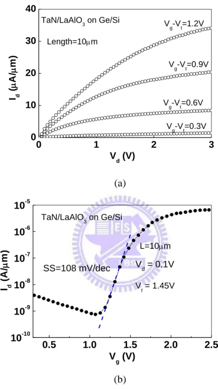
n-MOSFETs using LaAlO3 gate dielectric. Figs. 2.4(a) and 2.4(b) present the Id-Vd
and Id-Vg characteristics, respectively. Small sub-threshold swing (SS) of 108 mV/dec
and very low IOFF of 710-10 A/μm were measured. This small IOFF leakage and good
SS were vital for small EG and high mobility new channel MOSFET used for low
power Green Transistor application. Further improving ION/IOFF may be reached by
chemical interface passivation using H, S, or Se. It is noticed that the SS was one of
the best-reported data for gate-first Ge n-MOSFET [2-1]-[2-24] that was even better
than the TaN/TiLaO/SiO2/Ge/Si n-MOSFET using SiO2 interfacial layer at a smaller
EOT of 0.81 nm. Here the SS is expressed as [2-32]:
) 1 ( 10 ln i it dep C C C q KT SS (1)
where Cdep was the depletion capacitance density, Cit was the capacitance density
from charged interface traps and Ci was the gate capacitance density. The improved
SS at larger EOT was an indication of improved interface properties of LaAlO3 gate
dielectric on Ge/Si compared with previous TiLaO/SiO2 with an ultra-thin SiO2
interfacial layer on Ge/Si [2-22].
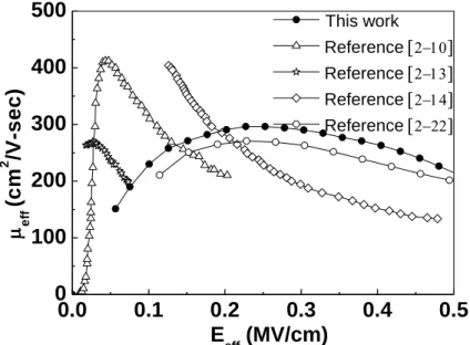
Fig. 2.5 shows mobility as a function of Eeff. The mobility was calculated
directly from the Id-Vg curves [35]. For comparison, the mobility data from related
literatures were also plotted [2-10], [2-13]-[2-14], [2-22]. The lower peak mobility
could be attributed to the remote phonon scattering in the high-κ dielectric that was
also found in high-κ/Si MOSFET. Therefore, an ultra-thin SiO(N) [2-33] or GeO2
[2-14]-[2-17], [2-19]-[2-20] interfacial layer was needed to further improve the peak
mobility and ION/IOFF. Although higher peak mobility values were published [2-10],
[2-13]-[2-14], the mobility decreased rapidly with an increase in Eeff due to the
interface scattering. However, the MOSFET was destined to operate at high Eeff due to
the small 1 nm EOT used for 45~32 nm nodes [2-34]. In sharp contrast, the Ge
n-MOSFET using LaAlO3 showed the superior high field mobility of 218 cm2/Vs at
0.5 MV/cm that was one of the best reported high-field mobility data for gate-first Ge
n-MOSFETs [2-1]-[2-24].
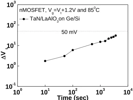
bias-temperature instability (BTI) testing. A small threshold-voltage shift (Vt) of 31
mV was measured at a 1.2 V gate overdrive (Vg-Vt) and 85oC for 1 hr. Table 1
summarizes and compares the important device parameters of metal-gate/high-Ge
n-MOSFETs [2-10], [2-13]-[2-14], [2-17]-[2-20], [2-22]. The TaN/LaAlO3/Ge/Si
n-MOSFET had superior high-field mobility of 218 cm2/Vs at 0.5 MV/cm, record low
SS of 108 mV/dec, small 1.6 nm EOT, very low IOFF of 710-10 A/μm, simple
gate-first process and useful for 12-in integration.
2.4. Conclusion
This study has demonstrated a high performance gate-first epitaxial Ge
n-MOSFET on Si. Using high-κ LaAlO3, this study achieved good device
performance of a record small SS and high mobility at high Eeff among reported
gate-first Ge n-MOSFETs, as well as the very low IOFF for low power application and
a small 1.6 nm EOT. The self-aligned, gate-first TaN/LaAlO3/Ge/Si n-MOSFETs had
Process Metal Gate High- EOT (nm) Ioff (A/m) SS (mV/dec) Peak Mobility (cm2/V-s) Mobility 0.5 MV/cm (cm2/V-s) [2-10] Gate-first TaN HfAlO 3.0 - 110 412 low [2-13] Gate-last Au GeO2 large - - 270 low
[2-14] Gate-first Al Al2O3+ GeO2 large 1.24x10⁻⁹ - 404 133
[2-17] Gate-first Al Al2O3+GeO2 large 9x10⁻¹⁰ - 488 363
[2-18] Gate-last Al GeO2(70-atm) large - 125 790 460
[2-19] Gate-last Al Al2O3+GeO2 large 7x10-11 193 804 269
[2-20] Gate-last Al SiO2+GeO2 large 8.3x10⁻¹⁰ - 540 201
[2-22] Gate-first TaN TiLaO+SiO2 0.81 3.5x10⁻¹⁰ 126 271 201
This
work Gate first TaN LaAlO3 1.6 7x10
-10
108 296 218
Table 2-1. Comparison of device integrity data for various metal-gate/high-κ Ge
-1.0 -0.5 0.0 0.5 1.0 1.5 2.0 2.5 0.0 0.5 1.0 1.5 2.0 EOT=2.6 nm 500oC RTA 550oC RTA 450oC RTA 500oC RTA 550oC RTA C ( F /c m 2 ) Voltage (V)
Control HfAlO on Ge/Si and Si
HfAlO/Si control 450oC RTA Vfb roll off Vfb = 1.46V V fb shift 1.2V
(a)
-2 -1 0 1 2 0.0 0.5 1.0 1.5 2.0 2.5 TaN/LaAlO3/Si Vfb = 0.41V 4500C RTA 5000C RTA 5500C RTA C ( F /c m 2 ) Voltage (V) Sweep from -2V to 2V TaN/LaAlO 3 on Ge/Si QM-CV Simulation EOT = 1.6 nm 4500C RTA V fb shift 0.9 V(b)
Fig. 2.1 C-V characteristics of (a) TaN/HfAlO/Ge/Si and control TaN/HfAlO/Si n-MOS capacitors and (b) TaN/LaAlO3/Ge/Si n-MOS capacitors at 100 kHz
-2.0 -1.5 -1.0 -0.5 0.0 10-8 10-7 10-6 10-5 10-4 10-3 10-2 10-1 100 LaAlO3 @4500C RTA LaAlO3 @5000C RTA
1.6-nm-EOT LaAlO3 @5500C RTA
J (A /c m 2 ) Voltage (V)
2.6-nm-EOT HfAlO @550oC RTA
(a) 0.8 1.0 1.2 1.4 1.6 1.8 2.0 10-5 10-4 10-3 10-2 10-1 100 101 102 103 104 25X Intel 45 nm node [2-34] TaN/LaAlO3 on Ge/Si J g @ 1 V + V fb | (A /c m 2 ) EOT (nm) Poly-Si/SiO2 Benchmark (b)
Fig. 2.2 (a) J-V characteristics of TaN/LaAlO3/Ge/Si and TaN/HfAlO/Ge/Si n-MOS
capacitors after 450oC~550oC RTA. (b) J-EOT characteristics of TaN/LaAlO3/Ge/Si n-MOS capacitors after550oC RTA.
(a)
(b)
(c)
Fig. 2.3 Cross-sectional TEM of (a) TaN/HfAlO/Ge/Si capacitor, (b) control
TaN
HfAlO
Ge
Si
5nm
4.0 nm
TaN
Si
HfAlO
5nm
4.0 nm
TaN
Si
HfAlO
5nm
4.0 nm
TaN
5nm
LaAlO
3Ge
Si
4.0nm
0 1 2 3 0 10 20 30 40 Vg-Vt=0.3V Vg-Vt=0.6V Vg-Vt=0.9V I d ( A/ m ) Vd (V) V g-Vt=1.2V Length=10m TaN/LaAlO 3 on Ge/Si
(a)
0.5 1.0 1.5 2.0 2.5 10-10 10-9 10-8 10-7 10-6 10-5 Vd = 0.1V L=10m I d ( A/ m ) V g (V) SS=108 mV/dec Vt = 1.45V TaN/LaAlO3 on Ge/Si(b)
Fig. 2.4 (a) Id-Vd and (b) Id-Vg characteristics of gate-first TaN/LaAlO3/Ge/Si
n-MOSFETs after 550oC RTA. The gate length and width are 10 and 100 m, respectively.
0.0 0.1 0.2 0.3 0.4 0.5 0 100 200 300 400 500 This work Reference Reference Reference Reference eff (cm 2 /V -s e c ) Eeff (MV/cm)
Fig. 2.5 Electron mobility vs. effective electric field of TaN/LaAlO3/Ge/Si
10
010
110
210
310
410
-110
010
110
210
3 nMOSFET, V g=Vt+1.2V and 85 0 C TaN/LaAlO3on Ge/Si
V
t
Time (sec)
50 mVChapter 3
Interfacial Layer Dependence on Device Property of
High-
TiLaO Ge/Si N-Type
Metal-Oxide-Semiconductor Capacitors at Small
Equivalent-Oxide Thickness
3.1. Introduction
Germanium (Ge) has attracted much attention for Metal-Oxide-Semiconductor
Field-Effect Transistor (MOSFET) [3-1]-[3-14] application due to both higher
electron and hole mobilities than Silicon (Si). However, the difficult challenges are
the high leakage current of small energy bandgap (EG) Ge and the poor interface
property with high dielectric-constant () material. To lower the leakage current, we
pioneered the defect free Ge-on-insulator (GOI or GeOI) [3-1] structure, and the
leakage current decreases with decreasing the Ge body thickness [3-5]. Nevertheless,
the degraded interface property is still a tough challenge especially for the Ge n-type
MOSFET (n-MOSFET) [3-6]-[3-12] at a small equivalent oxide thickness (EOT). The
interface property is highly dependent on high- dielectrics, where Al2O3 [3-1] and
La2O3 [3-8]-[3-11]show lower interface trap density than HfO2. This is related to the
different Metal-Oxygen-Ge and defect formations [3-11] after a rapid-thermal anneal
such as plasma nitridation,[3-4]-[3-8] NH3 treatment, SiH4 annealing and interfacial
GeO2 layer [3-8]-[3-10], [3-12]-[3-14] at larger EOT, but small EOT less than 1 nm is
needed for 32 nm node and beyond. In this paper, we have applied the ultra-thin GeO2
and SiO2 interfacial layers [3-15] into high- TiLaO [3-16] epitaxial-Ge/Si n-type
MOS (n-MOS) capacitors, where the ultra-thin body Ge of 5 nm is directly grown on
Si to reach low leakage current. The TiLaO gate dielectric has the merits of unique
negative flat-band voltage (Vfb) from La2O3 [3-17] and the much higher by adding
TiO2 [3-16]. Such negative Vfb is needed for low threshold voltage (Vt) MOSFET. The
control TaN/TiLaO/Ge/Si n-MOS capacitor without the ultra-thin GeO2 or SiO2
interfacial layer showed poor EOT and large Vfb degradation after a 550oC RTA,
which is required to activate ion-implanted source-drain in the MOSFET. Such
degradations are related to interface reaction and oxygen vacancy formation
[3-18]-[3-19] that are much improved by inserting the ultra-thin GeO2 or SiO2 [3-15]
interfacial layer. However, the high-TiLaO Ge/Si n-MOS capacitor with interfacial
GeO2 showed much poorer capacitance-voltage (C-V) hysteresis than that using SiO2
at a smaller EOT less than 1 nm. This is due to the Ge out-diffusion and intermixing
of high-TiLaO/GeO2 as observed by cross-sectional Transmission Electron
Microscopy (TEM) and Secondary Ion Mass Spectroscopy (SIMS).
3.2. Experimental procedure
capping layer were epitaxial grown on 6-in p-type Si substrate (10 ohm-cm) by
ultra-high-vacuum chemical-vapor-deposition (HUVCVD). After removing the native
oxide of Si-capping layer, various thick GeO2 or SiO2 and 5 nm high- TiLaO [3-16]
were deposited by physical vapor deposition (PVD) and followed by post-deposition
annealing (PDA) at 400oC in oxygenambient to improve gate dielectric quality. Here
the ultra-thin Si capping is used to prevent Ge oxidation and process loss, where no
interfacial Si was found by cross-sectional TEM after device process. Then a 50 nm
TaN was deposited and patterned to form the metal gate. The formed gate stack was
applied by a 550oC RTA that is needed for Ge n-MOSFET fabrication. Finally,
Aluminum (Al) was deposited on wafer backside to form the MOS capacitors. For
comparison, control device without GeO2 or SiO2 interfacial layer was also made. The
fabricated gate stack was examined by SIMS, TEM, X-ray Photoelectron
Spectroscopy (XPS) and C-V measurements to investigate the physical, chemical
bonding and electrical properties, respectively.
3.3. Results and discussion
Figure 3.1 shows the measured C-V characteristics of high- TiLaO Ge/Si
n-MOS capacitors with or without the interfacial GeO2 or SiO2 layer. For device
without the inserted GeO2 or SiO2 layer, both the capacitance density and Vfb were
severely degraded. Such V
fb roll-off at high temperature was previously reported due
capacitor with GeO2 or SiO2 layer shows much improved V
fb roll-off even after a
550oC RTA. Besides, the needed negative Vfb of -0.48 V is obtained and important for
low Vt Ge n-MOSFET. However, the device with GeO2 interfacial layer shows poorer
C-V hysteresis of 93 mV at 1.1 nm EOT than the much improved 19 mV hysteresis at
smaller 0.81 nm EOT for device using SiO2 interfacial layer, by taking account of
quantum-mechanical effect with parameters of Ge [3-7]. The C–V hysteresis and
negative Vfb value are among the best reported data for Ge n-MOS capacitors at the
smallest EOT and after a 550oC RTA [3-1]-[3-14],to our best knowledge.
We have used TEM to study the better electrical performance for device using
interfacial SiO2 layer. Figures 3.2(a) and 3.2(b) show the TEM images of
TaN/TiLaO/GeO2/Ge/Si n-MOS structure before and after a 550oC RTA. Sharp GeO2
interfacial layer of 0.76 nm thickness was found for as-deposited sample but becomes
blurred after the 550oC RTA. The high- layer is also thicker after the 550oC RTA,
where intermixing of high- TiLaO and GeO2 is observed. The thicker high- layer
explains the lower capacitance density after a 550oC RTA. In strong contrast, sharp
SiO2 interface shown in Fig. 3.2(c) is still preserved even after the 550oC RTA.
We have further used SIMS to study the large difference for devices with
different interfacial GeO2 and SiO2. Figures 3.3(a) and 3.3(b) show the measured
respectively. Severe Ge out-diffusion was found for device structure with interfacial
GeO2 layer after a 550oC RTA, while much improved Ge out-diffusion was achieved
using ultra-thin SiO2 interfacial layer even at a smaller 0.81 nm EOT.
The degraded interface property with ultra-thin interfacial GeO2 was also
examined by XPS. Figure 3.4 shows the Ge 2p3 XPS spectra of TiLaO/GeO2/Ge/Si
n-MOS structure before and after the 550oC RTA. The as-deposited sample shows a strong Ge peak at 1217.4 eV, and a small higher energy side peak is attributed to
Ge-O bonds of GeO2 [3-20]. However, this Ge-O peak becomes much weaker for the
sample after the 550oC RTA. This is consistent with the largely thinned GeO2 and
intermixed TiLaO/GeO2 interface found from cross-sectional TEM and the large Ge
out-diffusion measured by SIMS. The thinner interfacial GeO2 after the high
temperature 550oC RTA may be related to the measured reaction at 758~589K [3-21]:
GeO2(s) + Ge(s) 2 GeO(g) (2)
In contrast, the interface reaction between ultra-thin SiO2 layer and Ge is unfavorable
due to the much higher bond enthalpy of SiO2 (800 kJ/mol) than GeO2 (659 kJ/mol)
[3-22].
3.4. Conclusion
In conclusion, we have studied the high- TiLaO on Ge/Si MOS structure with
GeO2 and SiO2 interfacial layers. Low EOT of 0.81 nm, small C-V hysteresis of 19
device with ultra-thin interfacial GeO2 shows inferior device performance of larger
EOT and poor C-V hysteresis, which is due to the severe Ge out-diffusion through
GeO2 from SIMS profile, thicker gate dielectric from TEM observation and thinned
-3
-2
-1
0
1
2
0.0
0.5
1.0
1.5
2.0
2.5
3.0
3.5
C
(
F
/c
m
2)
Voltage (V)
TiLaO/SiO 2 on Ge/Si TiLaO/GeO 2 on Ge/Si TiLaO on Ge/Si Solid: 450oC RTA; Open: 550oC RTA100KHz Frequency
Fig. 3.1. C-V characteristics of TaN/TiLaO Ge/Si n-MOS capacitors with or without
the inserted GeO2 and SiO2 interfacial layer and after 450 or 550oC RTA.
(a)
(b)
(c)
Fig.3.2. Cross-sectional TEM images of TaN/TiLaO/GeO2/Ge/Si n-MOS capacitors
(a) before and (b) after 550oC RTA. (c) TaN/TiLaO/SiO2/Ge/Si n-MOS
0 1000 2000 3000 4000 101 102 103 104 105 106 107 108 In te n s it y ( C /S ) Sputter Time (S) Si 550oC RTA Si as-deposited Ge 550oC RTA Ge as-deposited O 550oC RTA O as-deposited Ta 550oC RTA Ta as-deposited Ge out-diffusion (a) 0 1000 2000 3000 4000 101 102 103 104 105 106 107 108 In te n s it y ( C /S ) Sputter Time (S) Si 550oC RTA Si as-deposited Ge 550oC RTA Ge as-deposited O 2 as-deposited O2 550oC RTA Ta 550oC RTA Ta as-deposited (b)
Fig. 3.3. SIMS profile of TaN/TiLaO Ge/Si n-MOS structure with inserted (a) GeO2
12107 1215 1220 1225 1230 1235 8 9 10 11 12 13 14 Ge-Ge as-deposited 550oC RTA In te n s it y ( C /S ) Binding Energy x103 Ge-O TaN/TiLaO/GeO 2 on Ge/Si
Fig. 3.4. The Ge 2p3 XPS spectra of TiLaO/GeO2/Ge/Si structure before and after
Chapter 4
High Performance of Ge n-MOSFETs Using SiO2
Interfacial Layer and TiLaO Gate Dielectric
4.1. Introduction
The Ge channel MOSFETs [4-1]-[4-11] have attracted much attention due to
higher bulk electron and hole mobilities than Si counterparts. Nevertheless, the
technical challenges for Ge MOSFETs are severe, which include the integration of
defect-free Ge on Si substrate, the large leakage current of small energy bandgap (EG)
Ge and the poor electron mobility at high effective electric field. The integration of
defect-free Ge on Si was demonstrated by us using wafer-bonded Ge-on-insulator
(GOI or GeOI) technology [4-1]. The leakage current of small EG Ge MOSFET is also
lowered by thinning Ge body thickness in GOI [4-5]. However, the electron mobility
degradation at high effective field is still a severe issue, which is especially important
for MOSFET at small equivalent-oxide thickness (EOT). In order to improve the
mobility, many interface passivation methods have been proposed such as NH3
surface treatment, SiH4 annealing [4-4], Si capping layer [4-6], [4-9] and GeO2
interfacial layer [4-7]-[4-8]. Unfortunately, these methods still got relative low
mobility at high effective field. The SiOx interfacial layer has been used for Ge
field mobility are still the major challenges for Ge n-MOSFET. In this paper, we
report high mobility at high effective field for Ge n-MOSFETs with small
capacitance-equivalent-thickness (CET), which was achieved by using higher
TiLaO dielectric [4-12]-[4-13] and SiO2 interfacial layer. In contrast, much degraded
CET and unwanted flat-band voltage (Vfb) shift were measured for control device
without the SiO2 interfacial layer.
4.2. Experimental procedure
After standard clean, an undoped 200 nm Si buffer, undoped 5 nm Ge and
undoped 1.5 nm Si capping layer were grown on p-type (100) Si wafers (5×1015 cm-3
doping) by ultra-high-vacuum chemical-vapor-deposition (HUVCVD) at 500oC and
5×10⁻⁴ torr. An ultra-thin 0.8 nm SiO2 was deposited by Physical Vapor Deposition
(PVD) using Electron-Beam Evaporation at the room temperature and 2×10⁻⁶ torr
pressure [3-14], where the native oxide of Si-capping layer was removed using dilute
HF solution. Here the Si-capping is to prevent the thin Ge loss during process, since
Ge can be oxidized by water and air similar to Si case and GeO2 is dissolvable by
water. No Si-capping layer was found by cross-section TEM after process. A 5 nm
thick TixLa1-xO (x~0.67) [3-12] with of 45 was deposited and followed by a 400oC
post-deposition anneal (PDA) in an oxygen ambient for 5 min. Then a 200 nm TaN
was deposited by PVD and patterned to form the metal gate. For comparison, the
25 KeV As+ion implantation was applied at a 5×10
15
cm
-2
dosage and 550oC RTA.
From the X-Ray Diffraction (XRD) study, the TiLaO is amorphous after 550oC RTA.
Finally, non-alloyed Al contact metal was added. The fabricated devices were
characterized by capacitance-voltage (C-V) and current-voltage (J-V) measurements.
4.3. Results and Discussion
In Fig. 4.1 we showed the C-V characteristics of TaN/TiLaO on Si-capped Ge/Si
capacitors after 450~550oC RTA. These devices showed severe degradations of
capacitance density, Vfb shift, and hysteresis after a 550oC RTA, which was related to
interfacial layer formation as found by TEM. However, this temperature is required to
activate the ion implanted dopants at source-drain of Ge MOSFET.
To address the interface reaction, we added an ultra-thin SiO2 interfacial layer
between high- and Ge. Figures 4.2(a) and 4.2(b) showed the C-V and J-V
characteristics of the TaN/TiLaO/SiO2 on Ge/Si n-MOS devices. Much smaller
unwanted Vfb shift and less interface states generation are reached than the devices
without SiO2 interfacial layer shown in Fig. 4.1. The good high- and interface
quality is also evident from the small C-V hysteresis of only 19 mV from -3 to 1 V
sweep. Such large difference is due to the dense and strong bonding SiO2 to prevent
the Ge out diffusion during the process, from SIMS measurements. Besides, a small
Figures 4.3(a) and 4.3(b) show the respective Id-Vd and Id-Vg characteristics. Good
transistor characteristics of relatively high drive current, small sub-threshold swing
(SS) of 126 mV/dec and a record low IOFF leakage of 3.5×10⁻¹⁰ A/m [4-6]-[4-8] were
measured simultaneously. This is due to the ultra-thin body (UTB) of conductive Ge
channel on Si substrate that is well predicted by UTB GOI MOSFETs [4-5]. Such low
leakage current is mandatory for future generation low power green transistor.
Figure 4 shows the electron mobility versus effective electric field, where the data
was directly derived from measured Id-Vg curves [4-15]. Good high field mobility at
0.5 MV/cm is 201 cm2/V-s [4-6]-[4-8] at a small 1.1 nm CET. The good high field
mobility is consistent with the needed negative Vfb, small C-V hysteresis and SS; here
the SS of 126 mV/dec is one of the best reported data for Ge n-MOSFET in literature
[4-1]-[4-11]. The good high field mobility is vital for MOSFET at a small EOT,
where a still high 0.65 V drain voltage is needed even for 11 nm node technology
according to ITRS.
4.4. Conclusions
We have demonstrated high performance epitaxial Ge n-MOSFET on Si using
higher TiLaO and SiO2 interfacial layer.Good device performance is reached in
terms of small CET, record low IOFF and the highest mobility at high effective electric
field. Besides, this self-aligned and gate-first transistor has the advantages of simple
-2 -1 0 1 2 0.0 0.5 1.0 1.5 2.0 2.5 3.0 450oC RTA From -2V to 2V 450oC RTA From 2V to 2V 500oC RTA From -2V to 2V 500oC RTA From 2V to 2V C
(
F /c m 2)
Voltage (V)TiLaO on Si-capped Ge/Si
100kHz frequency
550oC RTA From -2V to 2V 550oC RTA From 2V to 2V
Fig. 4.1. C-V and of the TaN/TiLaO on Si-Capped Ge/Si n-MOS capacitors after
![Fig. 1.3 Static dielectric constant versus band gap for candidate gate oxides [1-34].](https://thumb-ap.123doks.com/thumbv2/9libinfo/8100730.165167/27.892.204.649.141.474/fig-static-dielectric-constant-versus-band-candidate-oxides.webp)