國 立 交 通 大 學
電子工程學系 電子研究所
碩 士 論 文
高效能增強型砷化鎵金氧半場效電晶體元件
電性研究
The Electrical Characteristics of High Performance
Enhancement Mode GaAs
Metal-Oxide-Semiconductor Field-Effect-Transistor
Devices
研 究 生 : 黃昶智
指導教授 : 簡 昭 欣 教授
高效能增強型砷化鎵金氧半場效電晶體元件電
性研究
The Characteristics of High Performance Enhancement
mode GaAs Metal-Oxide-
Semiconductor Field-Effect-Transistor Devices
研 究 生 : 黃 昶 智 Student: Chang-Chih Huang
指導教授 : 簡 昭 欣 教授 Advisor: Dr. Chao-Hsin Chien
國 立 交 通 大 學
電子工程學系 電子研究所
碩 士 論 文
A Thesis
Submitted to the Institute of Electronics
College of Electrical Engineering and Computer Engineering National Chiao Tung University
in Partial Fulfillment of the Requirements for the Degree of Master
in Electronic Engineering August 2011
Hsinchu, Taiwan, Republic of China
i
高效能增強型砷化鎵金氧半場效電晶體元件
電性研究
學生: 黃昶智 指導教授: 簡 昭 欣 教授
國立交通大學
電子工程學系 電子研究所碩士班
摘要
在這篇論文中,我們首先研究以砷化鎵材料沉積氧化鋁介電層的電容其電性特徵。 較差的介電層品質會造成頻率響應/頻率分散( frequency dispersion), 延滯現象 ( hysteresis ), 平帶偏移( flab band shift ), 和不預期的低介電常數 (dielectric constant )。根據電性上的結果,在做過矽甲烷鈍化的電容展現出不只低的頻率分散而 且延滯現象也很小。我們相信做過矽甲烷鈍化的電容可以有效降低砷化鎵氧化物的形成。 為了證實我們的推論,我們利用電導的方式去萃取介面缺陷密度的分佈。接著,我們量 測原子層沉積氧化鋁介電層於矽甲烷表面鈍化之砷化鎵電容其可靠度,可以透過在不同 應力條件下捕捉/釋放電荷清楚了解不同介面的可靠度。我們觀察到矽甲烷表面鈍化後 的砷化鎵電容其可靠度有明顯的提升。接下來,我們在砷化鎵的不同晶相上做電性研究, 而發現在(111)A 的表面晶相上電容特性獲得了改善。當外加一個更大的正電壓,能帶可ii 以向下彎曲使表面的本質能階 Ei低於費米能階 EF。換句話說,砷化鎵能隙中間的介面缺 陷值降低,使費米能階可以移動到接近傳導能階。我們認為是不同晶相的表面的結構產 生的改善。 串聯電阻的大小是影響金氧半場效電晶體元件效能的重要因素,源極/集極的電阻 將會抑制最大驅動電流。我們利用CTLM這種結構討論其串聯電阻包括片面電阻率 (sheet resistivity )和接觸電阻率( contact resistivity )。根據這些電性特徵, 我們發現片面電阻率在 30keV&80keV 的離子佈植能量比在 50keV 的離子佈植能量來的小, 然而接觸電阻卻是相反。除此之外,由活化溫度的條件觀點來看,我們發現片面電阻率 在 850o C 比在 950o C 活化溫度來的小,然而接觸電阻卻是相反。我們統整可以找到最理 想的條件為 50keV 的離子佈植能量和活化溫度 850o C。但接面二極體在 950o C 活化溫度和 合金金屬 400o C30s 的條件下順向電流沒有明顯的被抑制。我們將片面電阻率、接觸電阻 率和歐姆接觸的條件優化,最後利用這些條件在不同晶相上將金氧半場效電晶體元件成 功製作出來並量測其特性。除此之外,我們也製作出砷化鎵嵌入鍺源極和集極的金氧半 場效電晶體元件並探討其特性。
iii
The Electrical Characteristics of High Performance
Enhancement mode GaAs Metal-Oxide-
Semiconductor Field-Effect-Transistor Devices
Student: Chang-Chih Huang Advisor: Dr. Chao-Hsin Chien
Department of Electronic Engineering and Institute of Electronics
National Chiao Tung University
Abstract
In this thesis, firstly, we have studied the electrical characteristics of GaAs capacitors
with Al2O3 dielectric. Poor dielectric quality results in frequency dispersion, hysteresis, flab
band shift, and unfavorable low dielectric constant. According to these electrical
characteristics, the passivation sample displayed not only small frequency dispersion, but also
small hysteresis. We believed that the surface treatment of SiH4 passivation can efficiently
diminish the formation of GaAs native oxide, and improve the effect of Fermi-level pinning
phenomenon. In order to confirm the speculation, we used the conductance method to extract
distributions of Dit for different interface passivation. Next, we measured the reliability of
silane surface passivated for gallium arsenide capacitors with atomic-layer-deposited Al2O3
gate dielectrics. A clear understanding of reliability of different interfaces, via charge
trapping/detrapping studies under different stressing condition, we observed the silane
passivation can improve the reliability of gallium arsenide capacitors. Then, we studied the
iv
substrates. The characteristics was improved on GaAs MOS capacitor with (111)A surface
orientation. When a larger positive voltage is applied, the bands bend more downward so that
the intrinsic level Ei at the surface crosses over the Fermi level EF. On the other hand, the
velue of Dit in the middle of energy bandgap was reduced, so the EF of surface on GaAs could
reach to near conduction level. We assumed that the improvement resulted from the different
structure of surface on orientation.
The series resistance is an importance factor for metal-oxide-semiconductor field effect
transistors (MOSFET) device performance. The source/drain ( S/D ) resistance will suppress
the maximum driving current. We discussed series resistance including sheet resistivity and
contact resistivity by CTLM structure. According to electrical characteristics, we discovered
that the sheet resistivity at 30keV&80keV is lower than 50keV implant energy. However, the
contact resistivity is just contrary. In addition, from the point of temperature, we found that
the sheet resistivity at 850℃ is lower than 950℃, and the contact resistivity is just contrary.
We can conclude the optimized condition for GaAs ohmic contact that was implanted at
50keV and the activation temperature at 850℃. But, the junction of forward current was not
suppressed significantly at activation temperature 950oC and alloy metal 400oC 30s. We
optimized conditions of sheet resistivity, contact resistivity, and Ohmic RTA time. Finally, we
used these conditions to fabricate metal-oxide-semiconductor field effect transistors with the
different surface orientation successfully and measured electrical characteristics. In addition,
we also fabricated GaAs MOSFET with embedded Ge source/drain and studied electrical
v
誌 謝
碩士兩年真的看似長,其實也只是轉眼瞬間的時間。學習的內容和大學沒有太多 的關係,想一想剛開始懵懵懂懂的樣子真的很有趣,經過跌跌撞撞,一點一滴的學習真 的讓我獲益良多。 首先,我最要感謝的就是我的指導教授簡昭欣博士,在報告上給我很多的指導和 鼓勵,讓我可以多方面分析去面對同一個問題去深入探討。接著就是宗佑學長、政庭學 長和信淵學長,謝謝你們的用心的指導和幫忙。無論在實驗上和分析資料上都給我很大 的協助,讓我得以順利完成這本論文。 謝謝國永學長介紹我到這個和諧的實驗室,在我碩一時就就開始教我一些研究方 法,了解該如何去架構論文,讓我能更快的進入狀況。另外,吳博(宏基)、禎晏和宗 霖學長很謝謝你們不辭辛勞的教導機台的操作和一些實驗技巧,使我在實驗上能成功的 完成。哲偉學長,當然不會忘記說你,謝謝你隨時在我一有問題時,給我立即的討論及 解答。 韋志和瑞國和你們一起共同打拼度過修課和學習機台,空閒時一起跑出去逛街、 聚餐、唱歌和看電影。這讓我能在研究後有個充電的空間,真的很謝謝你們這兩位夥伴 陪伴我這兩年。 除此之外,最要感謝我的家人,爸爸媽媽在旁的鼓勵是我最大的動力,讓我可以 全心全力的做研究,完成學業。妹妹的適時關心也讓我度過很多難關,謝謝妳!爺爺和 奶奶對我的關懷我心存感激及感動,您們都是我最大的支柱。我不會辜負你們的栽培, 我會盡全力讓家人過得更好!再次謝謝您們,有你們真好! 家豪學長恭喜你喜獲明珠,也預祝學長今年順利畢業!接下來研究就繼續傳承給 學弟,希望秉翰、俊池、哲鎮和兆志你們的實驗都能很順利,為實驗室做出貢獻就靠你 們了! 國小好朋友詩欣、尚鑫和贊能,國中好朋友勇志、偉旗和佑勳,高中好朋友鈺欣、vi 宇欣和世杰及大學好朋友泓緯、柏昇、嘉文和俊言,有你們的陪伴真的很棒,以後還是 繼續維持這友情牽絆! 最後謝謝曾經幫助過我的朋友們,謝謝你們。 黃昶智 2011 年 8 月
vii
Contents
Abstract (Chinese) ... i
Abstract (English) ... iii
Acknowledgement...v Contents...vii Table Captions ...x Figure Captions... xi
Chapter 1
Introduction
1.1 General Background ...1 1.2 Motivation ...21.3 Organization of the Thesis ...3
References...5
Chapter 2
Electrical characteristics of GaAs MOS capacitor
for different surface orientation
2.1 Introduction ...82.2 Experimental Procedures...10
2.2.1 Surface pre-treatment...10
2.2.2 ALD High-k Al2O3...10
2.2.3 Metal deposition...10
2.3 Effective reduction interfacial traps using thermal annealing... 10
viii
2.4.1 A C-V measurement result...12
2.4.2 Quasi-static C-V measurement result...13
2.4.3 Charge neutrality level (CNL) measurement...14
2.5 Admittance Behavior of GaAs MOS capacitor... 14
2.5.1 Conductance Method to Extract Dit... 14
2.5.2 Conductance method application of GaAs MOS capacitor... 16
2.5.3 High Temperature Measurement of GaAs MOS capacitor... 17
2.6 Electrical characteristics of GaAs MOSFET... 17
2.6.1 Introduction... 17
2.6.2 Source/Drain Ohmic Contact on GaAs... 18
2.6.3 Source/Drain Junction on GaAs... 20
2.6.4 MOSFET on GaAs with atomic-layer-deposited Al2O3 as gate dielectrics...21
2.7 Summary...23
References...25
Chapter3
Improved electrical characteristics of ALD-Al
2O
3/GaAs MOS capacitors
with silane
passivation
3.1 Introduction ...593.2 Experimental Procedures...61
3.2.1 Surface pre-treatment...61
3.2.2 ALD High-k Al2O3...61
3.2.3 Metal deposition...62
3.3 Capacitance-Voltage characteristics for GaAs(100) with silane passivation...62
3.3.1 Capacitance –Voltage characteristics for GaAs(100)... 62
3.3.2 Capacitance –Voltage characteristics for GaAs(100) with silane passivation.63 3.4 Effective reduction interfacial traps using thermal annealing...63
ix
3.4.1 Capacitance –Voltage characteristics for GaAs(100) PDA...63
3.4.2 Capacitance –Voltage characteristics for GaAs (100) with silane passivation.63 3.5 Admittance Behavior of GaAs MOS capacitor... 63
3.5.1 Conductance method application of GaAs MOS capacitor... 64
3.5.2 High Temperature Measurement of GaAs MOS capacitor... 65
3.6 Reliability characteristics of GaAs(100) with silane passivation... 66
3.7 Electrical characteristics of GaAs MOSFET...66
3.7.1 Introduction...66
3.7.2 Experimental Procedures...67
3.7.3 Result and conclusions...68
3.8 Summary... 68
References ... 70
Chapter4
GaAs nMOSFET with Embedded-Ge Source/Drain
4.1 Introduction ...974.2 Experimental Procedures...98
4.3 TiO2 interfacial layer on GaAs for low resistivity Contacts... 98
4.4 Ge-Source/Drain GaAs MOSFETs...99
4.5 Summary...100
References ... 101
Chapter 5
Conclusions and Suggestions for Future Work
5.1 Conclusions……...1055.2 Future Work...106
x
Table Captions
Chapter 2
Table 2.1 Integration CTLM of P-GaAs at 850 oC...50
Table 2.2 Integration juictions of P-GaAs(111)A...53
xi
Figure Captions
Chapter 1
Fig. 1.1 the device scaling roadmap of performance demonstrated by IMEC...7
Fig. 1.2 combination of III-V and Ge channel structure by Takagi et al. ...7
Chapter2
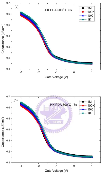
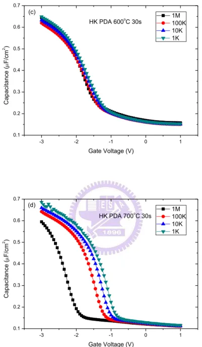
Fig. 2.1 The structure and process flow of MOS capacitor. ...28Fig. 2.2 C-V curve of MOS capacitor (a) 500 ℃, 30s (b)600 ℃, 15s...29
Fig. 2.2 C-V curve of MOS GaAs capacitor (c) 600 ℃, 30s (d)700 ℃, 30s...30
Fig. 2.3 C-V curve of MOS GaAs(100) capacitor (a) n-type (b) p-type...31
Fig. 2.4 C-V curve of MOS GaAs(111)A capacitor (a) n-type (b) p-type...32
Fig. 2.5 QSC-V curve of MOS GaAs capacitor (a) (100) (b) (111)A...33
Fig. 2.6 surface potentialψs versus gate voltage VG (a) (100) (b) (111)A...34
Fig. 2.7 Comparsion of Dit distribution of surface orientation effect (a) (100) (b) (111)A...35
Fig. 2.8 Comparison of Barrier verses Work Function (a) (100) (b) (111)A...36
Fig. 2.9 The band diagram of a typical MOS structure is illustrated, with surface potential in the semiconductor to periodically move up and down because of a small sinusoidal voltage on top of the static gate bias. ...37
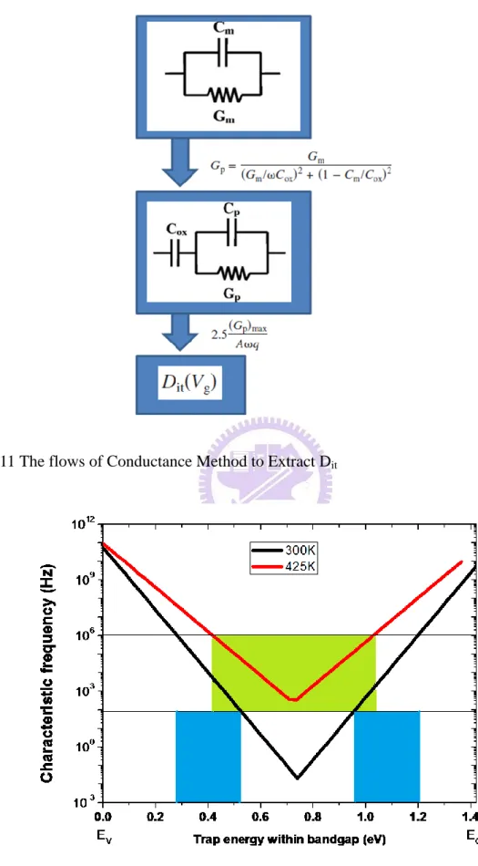
Fig. 2.10 Equivalent circuits for conductance measurements; (a) MOS capacitor, (b) simplified circuit, (c) measured circuit...37
Fig. 2.11 The flows of Conductance Method to Extract Dit...38
Fig. 2.12 Characteristic emission frequencies of trapped charge carriers in GaAs at the different temperature...38
Fig. 2.13 Gp/ as a function of frequency at 25℃(a) N-type GaAs(100) (b) P-type GaAs(100) ...39
Fig. 2.14 Gp/ as a function of frequency at 25℃ (a) N-type GaAs(111A) (b) P-type GaAs(111)A...40
Fig. 2.15 Multi-frequency C-V curve 425K(a) N-type GaAs(100) (b) P-type GaAs(100) ...41
Fig. 2.16 Multi-frequency C-V curve 425K(a) N-type GaAs(111)A (b) P-type GaAs(111)A.42 Fig. 2.17 Gp/ as a function of frequency at 150℃ (a) N-type GaAs(100) (b) P-type GaAs(100) ...43
Fig. 2.18 Gp/ as a function of frequency at 150℃ (a) N-type GaAs(111)A (b) P-type GaAs(111)A...44
Fig. 2.19 Comparsion of Dit distribution of different surface orientation...45
Fig. 2.20 III-V materials’ advantages...46
xii
Fig. 2.22 Contact Resistance Extraction...47
Fig. 2.23 SI-GaAs(111)A (a) 30keV&80keV 950oC (b) 30keV&80keV 850oC...48
Fig. 2.24 SI-GaAs(100) at 50keV 950oC...50
Fig. 2.25 P-GaAs(100) at 850 oC (a) 50keV (b) 30keV&80keV...51
Fig. 2.26 P-GaAs(111)A at 850 oC (a) 50keV (b) 30keV&80keV...52
Fig. 2.27 Junction current vs the voltage applied at N+ layer of the fabricated N+ /P GaAs junctions with Si implant at activity temperature 950oC(a) 30s (b)60s...54
Fig. 2.27 Junction current vs the voltage applied at N+ layer of the fabricated N+ /P GaAs junctions with Si implant at activity temperature 850oC(a) 30s (b)60s...55
Fig. 2.27 Junction current vs the voltage applied at N+ layer of the fabricated N+ /P GaAs junctions with Si implant at activity temperature 750oC(a) 30s (b)60s...56
Fig. 2.28 The scheme and process flow of GaAs MOSFET...57
Fig. 2.29 Id-Vg of enhancement mode GaAs n-MOSFET...58
Fig. 2.30 Id-Vd characteristics of enhancement mode GaAs n-MOSFET...58
Fig. 2.31 The effective mobility on E-mode GaAs n-MOSFET (a) Mobility with RSD (b) Mobility without RSD...59
Chapter 3
Fig. 3.1 The structure and process flow of MOS capacitor. ...73Fig. 3.2 Multi-frequency C-V curve (a) N-type GaAs(100) (b) P-type GaAs(100) ...74
Fig. 3.3 Extraction of VFB; (a) N-type VFB (b) P-type VFB...75
Fig. 3.4 Hysteresis C-V curve (a) N-type GaAs(100) (b) P-type GaAs(100) ...76
Fig. 3.5 Multi-frequency C-V curve(a) N-type GaAs(100)PDA (b) P-type GaAs(100)PDA..77
Fig. 3.5 Hysteresis C-V curve (c) N-type GaAs(100)PDA (d) P-type GaAs(100)PDA...78
Fig. 3.6 Multi-frequency C-V curve (a) N-type GaAs(100)with SiH4 passivation (b) P-type GaAs(100) with SiH4 passivation...79
Fig. 3.6 Hysteresis C-V curve (c) N-type GaAs(100) with SiH4 passivation (d) P-type GaAs(100) with SiH4 passivation...80
xiii
P-type GaAs(100) with SiH4 passivation and PDA...81
Fig. 3.7 Hysteresis C-V curve (c) N-type GaAs(100) with SiH4 passivation and PDA (d) P-type GaAs(100) with SiH4 passivation and PDA...82
Fig. 3.8 Multi-frequency C-V curve 300K (a) N-type GaAs(100)PDA (b) P-type GaAs(100)PDA...83
Fig. 3.9 Multi-frequency C-V curve 300K (a) N-type GaAs(100)with SiH4 and PDA (b) P-type GaAs(100) with SiH4 and PDA...84
Fig. 3.10 Gp/ as a function of frequency at 25℃ (a) N-type GaAs(100)PDA (b) P-type GaAs(100)PDA...85
Fig. 3.11 Gp/ as a function of frequency at 25℃ (a) N-type GaAs(100)PDA (b) P-type GaAs(100)PDA...86
Fig. 3.12 the Dit profile of GaAs(100) with SiH4 passivation at 300K...87
Fig. 3.13 Multi-frequency C-V curve 425K (a) N-type GaAs(100) (b) P-type GaAs(100) ....88
Fig. 3.14Multi-frequency C-V curve 425K (a) N-type GaAs(100)with SiH4 passivation (b) P-type GaAs(100) with SiH4 passivation...89
Fig. 3.15 Gp/ as a function of frequency at 150℃ (a) N-type GaAs(100) (b) P-type GaAs(100) ...90
Fig. 3.16 Gp/ as a function of frequency at 150℃ (a) N-type GaAs(100)with SiH4 and PDA (b) P-type GaAs(100) with SiH4 and PDA...91
Fig. 3.17 the Dit profile of GaAs(100) ...92
Fig. 3.18 the Dit profile of GaAs(100)with SiH4 and PDA at 425K...93
Fig. 3.19 High frequency capacitance–voltage (C–V) characteristics of MOS capacitors employing (a) Al2O3/P-GaAs and (b) Al2O3/Si/P-GaAs structures ...94
Fig. 3.20 The scheme and process flow of GaAs MOSFET...95
Fig. 3.21 Id-Vg of enhancement mode GaAs n-MOSFET...96
xiv
Chapter 4
Fig. 4.1 The scheme and process flow of GaAs MOSFET...102
Fig. 4.2 the I-V characteristics of the Al/TiO2/Ge structures...103
Fig. 4.3 Transfer characteristic for E-mode GaAs n-MOSFET with Ge-S/D...103
Fig. 4.4 Transfer characteristic for E-mode GaAs n-MOSFET with Ge-S/D by inserting TiO2
1
Chapter 1
Introduction
1.1 General Background
As Researchers continue to devotes on scaling transistors to conform with Moore’s
Law to sub-16-nm dimensions, it becomes very difficult to maintain the required device
performance. However, the increase in drive currents for faster switching speeds at lower
supply voltage is largely growing leakage current, which leads to a large standby power
dissipation. There is an important need to explore novel channel materials and device
structures that would provide nanoscale MOSFETs.
In recent years, Shrinking the dielectric thickness and channel length to get better
performance, but silicon-based complementary metal oxide semiconductor (CMOS) with
planar structures are approaching fundamental physical ultimate scaling limit. III-V
metal-oxide-semiconductor field transistors (MOSFET) provide high electron mobility and
low power consumption because of small effective mass. Then, due to availability of high
electron mobility, this has led to alternative channel materials that exhibit significantly
outperform the scaled Si MOSFET. The first GaAs MOSFET was reported by Becke and
White in 1965 [1]. Although SiO2 is used as the gate dielectric with an amount of interface
trap, the devices were operated successfully showing feasibility of this approach. But, SiO2 is
not right gate dielectric for III-V materials.
A variety of dielectrics have been investigated. For example, native oxides on GaAs as
gate dielectrics were studied. However, none of method is optimistic approach to achieve
2
researchers at Bell Labs discovered that sulfides are able to passivate GaAs interface [10-11].
In 1995, Prsslack and M. Hong reported in-situ deposition of Ga2O3(Gd2O3) dielectric on
GaAs surface by MBE[12-14]. Later, a serial of device works were carried out after the
breakthrough in material science, including GaAs depletion-mode, enhancement MOSFET,
GaAs complementary MOSFETs and GaAs power MOSFETs [15-18]. At the end of 2001, Ye
and Wilk started to use ALD to despite high-k such as Al2O3, HfO2 on GaAs. Later, detailed
interface studies were carried out to demonstrate the unpinning of Fermi-level in III-V
compound semiconductors using ALD high-k dielectrics [19-21].
IMEC had demonstrate the device scaling roadmap of performance as shown Fig.1.1.
III-V/Ge materials maybe be applied for sub-11-nm dimensions. Besides, In Fig. 1.2 is
combination of III-V and Ge channel structure according to Takagi et al.
1.2 Motivation
III-V metal-oxide-semiconductor field transistors (MOSFETs) have the main obstacle
that it is lack of high quality, thermodynamically stable gate dielectrics similar to SiO2 on
Silicon. So one key challenge in the III-V technology is that reduce the interface density of
states (Dit) that induce the Fermi level pining. The suitability of insulator/III-V interfaces for
MOSFETs applications has been addressed by appropriate interface control using some
surface passivation such as amorphous mixed oxide Ga2O3 (Gd2O3) and sulfur. However,
the methods are not suitable. It is because former’s cost is large and latter’s interface state densities are usually high. We have to research low cost and efficiently to reduce the density
of states.
In addition, we know these resistances affect on forward current of junction such as
contact resistances. If the value of resistance is higher, the forward currents decrease. And
then, the performance of devices will degrade. Therefore, we have to research reasonable
3
Although their small transport mass leads to high mobility, III-V materials have low
density of states (DOS) and the limited dopant level. Due to GaAs is almost lattice matched of
Ge. Therefore, Ge can be applied on n+-source/drain to provide electrons that maybe solute
these intrinsic issues.
1.3 Organization of the Thesis
In Chapter 2, we studied MOS capacitors and MOSFETs for different orientation on
GaAs (100) and (111)A surface. The results of MOS capacitors electrical characteristics on
GaAs (111)A surface are very different that compared to (100) surface. And then, we
discussed series resistance including sheet resistivity and contact resistivity. We explored
sheet resistivity and contact resistivity by CTLM structure. Next, we studied the junction for
different activity temperature. Finally, we optimize conditions of sheet resistivity, contact
resistivity, and Ohmic RTA time, and then, we applied these conditions on MOSFET.
In Chapter 3, we measured the electrical characteristic of GaAs capacitors with Al2O3
dielectric, including C-V measurement and conductance. We also studies electrical
characteristic of sample with silane passivation and PDA compared to sample without
passivation. Next, we analyzed reliability for silane passivation. A clear understanding of
reliability of the different interfaces, via charge trapping/detrapping studies under different
stressing condition. Finally, we applied this passivation on MOSFET.
In Chapter 4, we fabricate GaAs NMOSFET with embedded-Ge source/drain to solute
the issues of low density of states (DOS) and the limited dopant level. But n+-Ge contact has
been a challenge in EF pinning on metal/ n+-Ge interface. We used TiO2 interfacial layer to let
the electrical characteristics of GaAs NMOSFET with embedded-Ge source/drain be
imporved.
4
passivation, sheet resistivity, contact resistivity, junction and MOSFET. Finally, we gave some
5
Reference
[1] H. W. Becke, R. Hall, and J. P. White, “Gallium arsenide MOS transistor,” Solid-State
Electronics, vol. 8, pp. 813–823, 1965.
[2] H. Hasegawa, K. E. Forward, and H. L. Hartnagel, “New anodic native oxide of GaAs with improved dielectric and interface properties,” Applied Physics Letters, vol. 26, no. 10, pp. 567–569, 1975.
[3] D. Butcher and B. Sealy, “Electrical properties of thermal oxides on GaAs,” Electronics
Letters, vol. 13, pp. 558–559, 1977.
[4] O. A. Weinreich, “Oxide films grown on GaAs in an oxygen plasma,” Journal of Applied
Physics, vol. 37, no. 7, pp. 2924–2924, 1966.
[5] L. A. Chesler and G. Y. Robinson, “dc plasma anodization of GaAs,” Applied Physics
Letters, vol. 32, no. 1, pp. 60–62, 1978.
[6] N. Yokoyama, T. Mimura, K. Odani, and M. Fukuta, “Low-temperature plasma oxidation of GaAs,” Applied Physics Letters, vol. 32, no. 1, pp. 58–60, 1978.
[7] V. M. Bermudez, “Photoenhanced oxidation of gallium arsenide,” Journal of Applied
Physics, vol. 54, no. 11, pp. 6795–6798, 1983.
[8] S. D. Offsey, J. M. Woodall, A. C. Warren, P. D. Kirchner, T. I. Chappell, and G. D. Pettit, “Unpinned (100) GaAs surfaces in air using photochemistry,” Applied Physics Letters, vol. 48, no. 7, pp. 475–477, 1986.
[9] C. F. Yu, M. T. Schmidt, D. V. Podlesnik, E. S. Yang, and J. R. M. Osgood, “Ultraviolet-light-enhanced reaction of oxygen with gallium arsenide surfaces,” Journal
of Vacuum Science and Technology A: Vacuum, Surfaces, and Films, vol. 6, no. 3, pp.
754–756, 1988.
[10] B. J. Skromme, C. J. Sandroff, E. Yablonovitch, and T. Gmitter, “Effects of passivating ionic films on the photoluminescence properties of gaas,” Applied Physics Letters, vol. 51, no. 24, pp. 2022–2024, 1987.
[11] E. Yablonovitch, C. J. Sandroff, R. Bhat, and T. Gmitter, “Nearly ideal electronic properties of sulfide coated GaAs surfaces,” Applied Physics Letters, vol. 51, no. 6, pp. 439–441, 1987.
[12] M. Passlack, M. Hong, and J. P. Mannaerts, “Quasistatic and high frequency capacitance–voltage characterization of Ga2O3–GaAs structures fabricated by in situ molecular beam epitaxy,” Applied Physics Letters, vol. 68, no. 8, pp. 1099– 1101, 1996. [13] M. Hong, J. Kwo, A. R. Kortan, J. P. Mannaerts, and A. M. Sergent, “Epitax- ial Cubic
Gadolinium Oxide as a Dielectric for Gallium Arsenide Passivation,” Science, vol. 283, no. 5409, pp. 1897–1900, 1999.
[14] M. Passlack, M. Hong, J. P. Mannaerts, R. L. Opila, S. N. G. Chu, N. Moriya, F. Ren, and J. R. Kwo, “Low Dit thermodynamically stable Ga2O3-GaAs in- terfaces: fabrication,
6
Feb. 1997.
[15] F. Ren, M. Hong, W. S. Hobson, J. M. Kuo, J. R. Lothian, J. P. Man- naerts, J. Kwo, S. N. G. Chu, Y. K. Chen, and A. Y. Cho, “Demonstration of enhancement-mode p- and n-channel GaAs MOSFETs with Ga2O3(Gd2O3)As gate oxide,” Solid-State Electronics, vol. 41, pp. 1751–1753, 1997.
[16] Y. C. Wang, M. Hong, J. M. Kuo, J. P. Mannaerts, J. Kwo, H. Tsai, J. J. Krajewski, Y. K. Chen, and A. Y. Cho, “Demonstration of submicron depletion-mode GaAs MOSFETs with negligible drain current drift and hysteresis,” IEEE Electron Device Letters, vol. 20, pp. 457–459, 1999.
[17] M. Hong, J. N. Baillargeon, J. Kwo, J. P. Mannaerts, and A. Y. Cho, “First demonstration of GaAs CMOS,” Compound Semiconductors, 2000 IEEE International
Symposium on, pp. 345–350, 2000.
[18] Y. C. Wang, M. Hong, J. M. Kuo, J. P. Mannaerts, H. S. Tsai, J. Kwo, J. J. Kra- jewski, Y. K. Chen, and A. Y. Cho, “Ga2O3(Gd2O3)/GaAs power MOSFETs,” Electronics
Letters, 1999.
[19] Y. Xuan, H. C. Lin, P. D. Ye, and G. D. Wilk, “Capacitance-voltage studies on enhancement-mode InGaAs metal-oxide-semiconductor field-effect transis- tor using atomic-layer-deposited Al2O3 gate dielectric,” Applied Physics Letters, vol. 88, no. 26, p. 263518, 2006.
[20] Y. Xuan, H. Lin, and P. D. Ye, “Simplified surface preparation for GaAs pas- sivation using atomic-layer-deposited high-k dielectrics,” IEEE Transactions on Electron Devices, vol. 54, pp. 1811–1817, Aug 2007.
[21] Y. Xuan, H. Lin, and P. Ye, “Capacitance-voltage characterization of atomic- layer-deposited Al2O3/InGaAs and Al2O3/GaAs Metal-Oxide-Semiconductor structures,” ECS Transactions, vol. 3, no. 3, pp. 59–69, 2006.
7
Fig. 1.1 the device scaling roadmap of performance demonstrated by IMEC
8
Chapter 2
Electrical characteristics of GaAs
MOS capacitor for different surface
orientation
2.1 Introduction
In order to continue the scaling of silicon-based CMOS and maintain the historic
progress in information processing and transmission, innovative device structures and new
materials are required. A channel material with high mobility and therefore high injection
velocity can increase ON current and reduce delay. Currently, strained-Si is the dominant
technology for high performance MOSFETs. However, looking into future high mobility
III-V materials can offer several advantages over even very highly strained Si.
The III-V compound semiconductors such as GaAs have high electron mobility, high
breakdown field, low power consumption and wide band gap engineering [1, 2, 3]. Recently,
GaAs is one of great importance for scientific understanding of III-V interface and GaAs
compound semiconductor devices are applied as photodiodes, high electron mobility
transistors (HEMT), and other high-frequency devices [4]. But the poor quality of the
insulator/ substrate interface deposited such as SiO2 and Si3N4 degraded the performance of
MOSFET. Therefore, the literature on the subject that research efforts on achieving low
interfacial density of states (Dit) covers the past 40 years. The different surface orientation
have different density of states (Dit), the researchers discovered that the Fermi-level on
9
demonstrated that Fermi-level pining is not an intrinsic property, but the orientation
dependent.
The deposition mechanism of atomic-layer-deposited (ALD) is like chemical vapor
deposition (CVD), but is a thin film growth technique that two sequential, self-limiting
surface reaction between gas precursor such as tetrakis (ethylmethylamino) hafnium
( TEMAH, Hf[N(C2H5)(CH3)]4 ) and trimethylaluminum ( TMA, Al(CH3)3 ). ALD is a widely
used insulator as gate dielectric due to its good insulated properties, grown films are
conformal, pin-hole free, chemically bonding to reduce interfacial trap densities. After all,
ALD is one of the CVD, so thermal annealing can further improve the quality of dielectric.
Meanwhile, during high temperature process it is important to inhibit the loss of As within the
GaAs substrate and also suppress the formation and subsequent incorporation of native oxides.
The impact of thermal annealing on the properties of high-k/III-V interface has been
researched [7].
This Electrical characteristics, such capacitance-voltage ( C-V ) and conductance
characteristics, are regularly used in research and development to understand important
parameters of MOS capacitor and MOSFETs. For example, capacitance-voltage (C-V)
measurements are widely used to quantitatively study the MOS structures. There are several
important parameters in evaluating high-k dielectrics on novel channel materials, such as
hysteresis, frequency dispersion, and flat band shift and the dielectric/Ⅲ-Ⅴ interface quality.
C-V method is powerful to study the properties of the MOS structure, especially to explore
the issues with interfacial layers. Otherwise, the C-V and conductance characteristics are the
methods of choice to extensively study the interface characteristic because of the inherent
10
2.2 Experimental process
2.2.1 Surface clean
MOS capacitor sample was prepared on high Si-doped (p-type, 1~5×1017 cm-3 and
n-type, 1~5×1017 cm-3) GaAs with (100) and (111)A crystal orientation substrates. We have
three clean steps. At first, the GaAs was rinsed in the diluted HCl ( HCl : H2O = 1 : 3 )
solution for 3 min for native oxide removal, followed by rinsed in deionized water ( D.I.
water ) for 5 min. Second, the GaAs was rinsed in the diluted NH4OH ( NH4OH : H2O = 1 :
10 ) solution for 10 min for excess elemental arsenic removal, followed by rinsed in D.I.
water for 5 min. Third, the GaAs was rinsed in the (NH4)2S solution at room temperture for 10
min for ex-situ surface passivation, followed by rinsed in D.I. water for 5 min.
2.2.2 ALD High-k Al2O3
The samples mounted in the ALD chamber and gave 20 trimethylaluminum (TMA)
precursor pulses for reducing residual native oxide. And then, the Al2O3 gate dielectric was
deposited by ALD at 250 ℃, followed by post deposition annealing ( PDA ) in a N2 ambient.
Thermal annealing can further improve the quality of dielectric.
2.2.3 Metal deposition
Thermal evaporated 400 nm Al were patterned as gate electrodes through the
lithography. Finally, e-beam evaporated Ti/Pt/Au (50 Å /300 Å /1800 Å ) for p-type and
Ni/Ge/Au (300 Å /700 Å /1800 Å ) for n-type was deposited as backside contact.
The complete process flow was shown in Fig. 2.1. The electrical characteristics of
Al/Al2O3/p-GaAs/TiPtAu and Al/Al2O3/ n-GaAs/NiGeAu MOS capacitors were measured
using an HP4284 and HP4200, respectively.
2.3 Effective reduction interfacial traps using thermal annealing
11
dielectric. Meanwhile, during high temperature process it is important to inhibit the loss of As
within the GaAs substrate and also suppress the formation and subsequent incorporation of
native oxides.
The impacts of initial GaAs post-deposition annealing have been investigated. We used
four conditions of PDA to optimize better post annealing condition that efficiently reduced
native oxide. Reducing the high density of states on oxide/GaAs, particularly those near the
GaAs midgap region, resulting in serious Fermi-level pinning, and thus preventing a proper
inversion response required for the inversion-channel GaAs MOSFETs, is an important issue.
In this work, the interfacial traps are qualitative by performing C-V measurement. We
designed that post annealing at 500 ℃ for 30s, 600 ℃ for 15s, 600 ℃ for 30s and 700 ℃ for
30s on samples to find the optimal condition to lead to significant reduction of density of
states.
Capacitance-Voltage (C-V) characteristics of Al2O3/p-GaAs MOS capacitances
annealed under various conditions have been summarized in Fig. 2.2 : (a) annealing at 500 ℃
for 30s, (b) at 600 ℃ for 15s, (c) at 600℃ for 30s, and (d) at 700 ℃ for 30s. All the C-V
curves were measured by varies frequency (1kHz ~ 100kHz). According to these figures, we
can find that post annealing at 600 ℃ for 15s on sample had better electrical characteristics.
Annealing at 500 ℃ for 30s on sample didn’t bend banding to accumulation that value of
capacitance was low compared to other samples. Annealing at 600 ℃ for 30s and at 700 ℃
for 30s on samples had obvious stretch out behavior.
In summary, following to these characteristics of Capacitance-Voltage, we can optimize
the condition that post annealing at 600 ℃ for 15s on sample had better electrical
characteristics. It’s can significantly reduce native oxide, and then efficiently move Fermi-level.
12
2.4 Capacitance-Voltage characteristics for different surface
orientation
2.4.1 A C-V measurement result
First of all, we exhibit the basic properties of the GaAs (100) p-type and n-type MOS
capacitor C-V curves with multi-frequency, as shown in Fig. 2.3 (a) and (b), respectively.
The quantities of measured capacitances could be used to evaluate the quality of high-k
dielectrics and insulator-semiconductor. I defined frequency dispersion ratio≡∆C . The
equation of ∆C is reproduced according to Eq.(2.1)
∆C ≡ (C (@1kHz) – C (@100kHz) )/ C (@1kHz) ( 2.1)
The p-type GaAs (100) frequency dispersion (3.34%@-3V) are more excellent than
n-type GaAs (100) frequency dispersion (9.99%@+3V). We believed that should be a large
amount of density of states (Ga-Oxide) existed in upper half interfaces of bandgap. It slows
the Fermi-level is pinned at the upper half interface of bandgap when we supply voltage to
gate.
After introducing capacitance-voltage curves of GaAs (100), Fig. 2.4 (a) and (b) show
the MOS capacitor C-V curves of the GaAs (111)A p-type and n-type that is different
crystalline surface. The figures compare to Fig. 2.3 (a) and (b), n-GaAs (100) samples can’t
reach accumulation even at +3V applied to the gate. This case is because the Fermi-level is
pinned for a large amount of interface density of states. The MOS capacitor for n-GaAs
(111)A revealed C-V behavior can reach accumulation and had low stretch-out in depletion.
The p-type GaAs (111)A frequency dispersion is 3.08% (@-3V) and n-type GaAs (111)A
frequency dispersion is 8.28% (@+3V). The values revealed interface of states GaAs(111)A
13
2.4.2 Quasi-static C-V measurement result
Interface trapped charge, also known as interface traps or states are attributed to
dangling bonds at the semiconductor/insulator interface. GaAs is a large bandgap material.
Therefore, there is a large density of very slow interface states inside the GaAs semiconductor
bandgap. Quasi-static C-V provides information only on the interface trapped charge density,
but not on their capture cross section. The quasi-static C-V for different surface orientation
was shown in Fig. 2.5 (a) and (b) and calculating the surface potentialψs is a function of gate
voltage that surface potential was calculated by Berglund method. Berglund is given by
Eq.(2.2)
where CQSCV is the quasi-static C-V curve as a function of gate voltage. Integration from VG1
= VFB makes = 0, because band bending is zero at flatland. Integration from VFB to
accumulation and from VFB to inversion gives the surface potential across the energy bandgap
range. Fig. 2.6 displays the calculated result, surface potentialψs versus gate voltage VG.
According to Fig. 2.6, we can obviously know that these experimental results
conclusively demonstrate that Fermi-level on the GaAs (111)A surface is indeed unpinned and
Fermi-level pinning is not an intrinsic property of GaAs, but is orientation dependent thus
related to surface chemistry.
Otherwise, Utilizing high-frequency C-V curve and quasi-static C-V to extract Dit as a
function of gate voltage by high-low frequency method is described in Eq. (2.3).
where the value of Cox is defined on accumulation of quasi-static C-V. After Dit extracted by
high-low frequency method and x-axis conversion by surface potential ψs versus gate voltage
14
According to the Fig. 2.7 (a) and (b), we understand the difference between (111)A
orientation and (100) orientation. It is the reason that the performance of GaAs on (111)A
applied for MOSFETs is quite good compared to (100) orientation.
2.4.3 Charge neutrality level (CNL) measurement
The explanation of the Fermi level pinning phenomenon was first proposed by Bardeen,
the pining point was assumed to take place at the charge neutrality level (CNL) of the surface
states. Furthermore, extending this idea, Cowley and Sze derived the following well-known
equation for a M-S system.
(2.4)
Where is the location of the CNL measured form the vacuum level given by
with known c2 and c3 from experiments of varying .
First, we found different metals such as Ti, Au, and Pt to extract those schottky barrier
heights that we use Capacitance-Voltage method to get . The experimental results of the
metal-n-type GaAs system are shown in Fig. 2.8. The slope is c2 and the intercept is c3.
Spicer et al. discovered that CNL) in GaAs is separately 0.5eV and 0.7eV above
the valence band maximum (VBM) by photoemission and other experiments. However,
According to experiment results, eV for GaAs(100) and eV for
GaAs(111)A were not significantly different.
2.5
Admittance Behavior of
GaAs MOS capacitor
2.5.1 Conductance Method to Extract Dit
The conductance method is one of the most sensitive methods to determine Dit, so it is
the means of choice to extensively study the interface passivation. Through understanding of
the conductance method allow proper extraction of the interface trap across the bandgap. First
15
only is contributed from interface density and the band diagram of MOS capacitor is
showed in Fig. 2.9. Where is a gate voltage VG applied between the metal and the
semiconductor, which fixes the value of the surface Fermi level. The C-V measurements
consist in applying on top of the static gate bias voltage a small sinusoidal voltage with
frequency f and amplitude of 25 mV. This small periodic gate voltage causes the bands and
the surface potential in the semiconductor to periodically move up and down, causing the
interface traps lying around the value of the surface potential to fill and empty. Only if the
traps around the surface potential have a characteristic response time that is of the order of the
measurement frequency f can they interact with the measurement ac signal and affect the total
impedance of the MOS capacitor. The conductance uses a simplified equivalent circuit of the
capacitance and the parallel conductance, as seen in equivalent circuit model of Fig. 2.10. It
consists of the oxide capacitance Cox, the semiconductor capacitance Cs, and the interface
state capacitance Cit. The capture-emission of carriers by Dit is a losing process, represented
by the resistance Rit. It is convenient to replace the circuit of Fig. 2.10(a) by Fig. 2.10(b),
where Cp and Gp are given by
where Cit = q2Dit , ω=2πf, f is measurement frequency, and = RitCit, the characteristic
emission frequencies of trapped charge carriers, given by .
Equation (2.5) and Equation (2.6) is valid for an interface trap with single energy level in the
bandgap. In reality, interface traps are continuously distributed across the bandgap. If the time
constant dispersion and trap energy level distribution across bandgap are taken into account,
eq. (2.6) is modified:
16
When Gp/ is plotted as a function of f, the maximum appears at f , and at that
maximum
(2.8)
Gp/ plots are repeated at different gate voltages to scan trap energies to obtain an interface
state density distribution across the bandgap. By utilizing eq. (2.9), can be determined
from the measurement ( ) by eliminating the oxide capacitance.
(2.9)
The flows of conductance method to extract Dit in Fig. 2.11.
2.5.2 Conductance method application of GaAs MOS capacitor
It is worthy to note that according to the emission time constant ( ), the
behavior of interface trap time constant as a function of temperature determines the part of
interface traps in the bandgap observable in the MOS admittance characteristic. That is, traps
located nearer to midgap become observable for higher temperatures while traps more located
toward the band edges become observable for lower temperature. We assumed the capture
cross section σ = 1×10-15 cm2 and plotted the characteristic emission frequencies of trapped
charge carriers in GaAs at the different temperature as a function of the position of the trap in
the energy bandgap.For high band gap GaAs, midgap traps are not able to be observed at
room temperature; if increasing the temperature, the observable energy windows shift toward
the midgap as shown in Fig 2.12, where the effective density of states of the conduction (Nc)
and the valence (Nv) bands, electron and hole thermal velocity, change in GaAs bandgap with
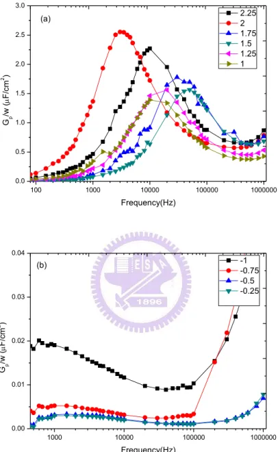
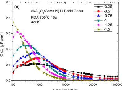
temperature are all taken into account. Fig 2.13 and Fig. 2.14 illustrates the Gp/ versus f
plots of MOS capacitor for different orientation and measurement is performed at room
17
bandgap where interface states are able to capture and emission with the small signal AC bias.
The peak value of each Gp/ curve corresponds to the interface state density and thus Dit as a
function of gate voltage can be plotted. Then, the equation combined with
the value of maximum value of Gp/ transforms the Dit (VG) into Dit (E) plot.
2.5.3 High Temperature Measurement of GaAs MOS capacitor
In order to obtain the full distribution of Dit in the bandgap, conductance method is
applied at high temperatures. The multi frequency CV characteristics measured at 423K are
shown in Fig. 2.15 and Fig.2.16 for different orientation. Fig. 2.17 and Fig.2.18 Gp/ curves
are shown at the gate voltages Fermi level is near the midgap where interface states are able to
capture and emission with the small signal AC bias. The peak value of each Gp/ curve
corresponds to the interface state density and thus Dit as a function of gate voltage can be
plotted. We interpret the largest Gp/ω value to represent Dit at the specific position in bandgap.
the Dit profile of each sample for GaAs(100) is demonstrated in Fig 2.19 compared to
GaAs(111)A.
According to these figures, we saw that Dit was not high for middle of the bandgap
obviously for n-type GaAs(111)A and p-type GaAs(111)A compared to the GaAs orientation
of (100). Once again, the electrical characteristics proved that the Fermi level pinning is not
an intrinsic property of GaAs.
2.6 Electrical characteristics of GaAs MOSFET
2.6.1 Introduction
In general, the condition of suitable gate dielectric on MOSFET will require: (a) the
oxides do not react with the substrates. (b) The band offset of the oxide on the semiconductor
is required to have over 1eV to inhibit leakage.
18
performance than Silicon. In particular, Ge and III-V based are promising material to use in
place of conventional Si MOSFETs. Recently, high-k/Ge p-MOSFET characteristics have
been reported have high performance characteristic recently [9-10]. However, Ge
n-MOSFETs remains have challenging because of the resulting from low electron mobility
and the asymmetrical distribution of interface states that result in the Fermi level (EF) pinning.
In addition, III-V materials have higher electron mobility than Ge, we showed some III-V
materials’ advantages in Fig. 2.20. In present, the several promising MESFET and n-MOSFET device characteristics based on III-V channels have been continually
demonstrated [11-16], and their performances even exceeded the strained-Si transistors at the
nano-scale devices [17]. In order to obtain the superior III-V device performance, it is
essential to achieve the unpinned oxide/substrate interface.
In this chapter, we fabricated the circular transmission line method (CTLM) for
analyzing contact and sheet resistivity. And then, we fabricated the junction of different
conditions. After optimizing the conditions of CTLM and junction, we also succeeded to
fabricate the enhancement-mode (E-mode) GaAs n-MOSFET with ALD- Al2O3 gate
dielectrics on the GaAs substrate.
2.6.2 Source/Drain Ohmic Contact on GaAs 1. Introduction
The resistance is an importance factor for metal-oxide-semiconductor field effect
transistors (MOSFET) device performance. The contact resistance is the most importance
among series resistances.
How to decide it is a good contact? The ohmic contact is a right method to determine.
Ohmic contacts have a linear current-voltage characteristic. The contacts have to be able to
supply the necessary device current, and the voltage drop across the contact should be small
compared to the voltage drops across the active regions. We fabricated the circular
19
W≠L of TLM can be avoided with circular test structure [18], including of a conducting circular inner region of radius r, a gap of width d, and a conducting circular outer region R in
Fig. 2.21. The total resistance between the internal and the external contacts is
, LT=
where I and K are the Bessel functions of the first order. Due to L 4LT, the Bessel function
ratios I0/I1 and K0/K1 tend to unity and RT simplifies to
In the circular transmission line test structure, due to r d, the equation becomes
, where C=
For d / r 1, the above equation simplifies to
, LT=
According to above equation, we firstly measured the relationship of RT and d, and find
line to fit it. The ρs and can be extracted. Finally, the value of ρc utilizes LT to obtain in
Fig. 2.22.
2. Experimental Procedures
The samples, firstly, were implanted the Silicon doses 1 × 1014 cm-2 at 50 keV After
deposit SiO2 capping layer, activation was using RTA at 750℃,850℃ and 950℃ for 15 s in
N2 ambient. Then, we used Acetone to remove metal-organic residues and the metal of
Ni/Ge/Au ( 30 nm/70 nm/180 nm ) was deposited by using E-gun system and lift-off process,
the CTLM structure in Fig. showed. Alloy metal was formed by RTA at 400 ℃ for 30s.
3. Results and Discussions
20
limiting, so we remove the condition of 750℃. We designed the conditions of different
activity temperature and implant energy on SI-(111)A substrate in shown Fig. 2.23 (a), (b), (c),
(d) and Table 1.
In these result, from the point of implant energy, we discovered that the sheet
resistivity at 30keV&80keV is lower than 50keV implant energy. However, the contact
resistivity is just contrary. In addition, from the point of temperature, we found that the sheet
resistivity at 850℃ is lower than 950℃, and the contact resistivity is just contrary. We can
conclude the optimized condition for GaAs ohmic contact that was implanted at 50keV and
the activity temperature at 850℃. Fig. 2.24 show the optimized condition on SI-(100) GaAs
substrate.
Next, we only designed the conditions of different implant energy for 850℃in shown
Fig.2.25, Fig. 2.26 and Table2. It is because that some of condition for 950℃showed current
characteristics couldn’t limiting( sheet resistivity is large ). Similarly, the optimized condition for GaAs ohmic contact was implanted at 50keV and the activity temperature at 850℃.
2.6.3 Source/Drain Junction on GaAs 1. Introduction
One of the most important properties is that their conductivity can be controlled by
adding dopants. The conduction mechanisms for a metal on n-type semiconductor are
described. For the low-doped semiconductor, the current mechanism is thermionic emission
(TE). For the high-doped N+, the width was sufficiently narrow for tunneling directly, known
as field emission (FE). In the intermediate-doped range, thermionic-field emission (TFE)
dominates. Although many exciting results on GaAs MOS capacitors and enhance mode
GaAs MOSFETs without source/drain implantation have been reported [19-21], and also the
cost is higher and the throughput is lower. GaAs material have a challenge in fabricating is
dopant’s low activation efficiency. It is because common source such as Si or Ge can replace either Ga atom or As atom to be donor or acceptor, respectively [22]. Hence, the net donor
21
concentration would be the number of Si atoms occupying the Ga minus the number of Si
atoms occupying the As. In order to increase the number of Si atoms occupying the Ga and
increase the activation efficiency, we design the conditions of different activity temperature
including 750℃, 850℃ and 950℃.
2. Experimental Procedures
In GaAs Junction fabrication, we used PECVD to deposit SiO2 420 nm as isolation
layer, and then, we defined the Si implantation regions by photolithography, which were
implanted the doses 1 × 1014 cm-2 at 50keV . After deposit SiO2 encapsulation layer, S/D
activation was using RTA at different temperatures in N2 ambient. the metal of Ni/Ge/Au
( 30 nm/70 nm/180 nm ) was deposited at the S/D region by using E-gun system and lift-off
process. Alloy metal was formed by RTA at 400 ℃ for 30s and 60s.
3. Results and Discussions
The GaAs P(111) N+/P junction current-voltage characteristic with Si implantation are
shown in Table 3 and Fig. 2.27 measured by 4200. The alloy metal annealing time by RTA is
30s and 60s was also examined. From the experiments, we can conclude the optimized
condition for GaAs Ohmic contact that was annealed at 400°C for 30s. In addition, we found
thatthe ratio of forward to reverse current at this N+ /P junction is achieved to be as high as
I forward / I reverse=107, indicating an activation temperature of 950 °C is enough to activate Si in
GaAs and a high quality N+ /P junction. The reason is because that the defect was repaired,
the junction reverse current could be reduced.
2.6.4 MOSFET on GaAs with atomic-layer-deposited Al2O3 as gate dielectrics
GaAs is one of materials for high performance due to its high electron mobility, high
saturation velocity, and wide bandgap. GaAs MOSFET can be applied on a sensitive test. In
this section, we fabricate GaAs MOSFETs for different orientation include (111)A and (100).
In GaAs MOSFET fabrication, we used ALD and PECVD to deposit Al2O3 10 nm and
22
regions, which were implanted the doses 1 × 1014 cm-2 at 50 keV and 1 × 1015 cm-2 at 60 keV,
respectively. S/D activation was using RTA at 850℃ for 10 s in N2 ambient. And then the
sample was cleaned by diluted HCl, diluted NH4OH, (NH4)2S solution. After surface cleaning,
the sample was loading into the ALD chamber, followed by surface pretreatment with TMA
pulse 20 cycles. Next, the Al2O3 gate dielectric was deposited by ALD at 250 ℃, followed by
PDA at 600 °C for 15 s in an N2 ambient. Thermal coatered Al about 4000 Å were patterned
as T-gate electrodes through the lithography. After excavating the S/D contact holes, the
tri-layer of Ni/Ge/Au ( 30 nm/70 nm/180 nm ) was deposited at the S/D region by using
E-beam system and lift-off process, followed by PDA at 400°C for 60 s in an N2 ambient to
form Ohmic contact. The fully process flow of GaAs MOSFET was shown in Fig. 2.28.
Fig. 2.29 illustrates the ID-VG transfer characteristic of 4μm gate length for E-mode
ALD-Al2O3/GaAs (111)A nMOSFET with TMA 20-cycles-pulse pretreatment and the ratio
Ion (ID at VG = 3V, VD = 2V)/Ioff (ID at VG = 0V, VD = 2V) is 2.8×10⁵. For device with the gate
length/width of 4/100 μm, the value of Vth was 0.895 V which is extracted by linear
extrapolation.
In Fig. 2.30, the well saturation and pinch-off characteristics were presented in ID-VD
curves with the gate drive VG ranging from 0 to 3 V in steps of 0.5 V display and the
maximum drain current was 46 μA/ μm measured at VG = 3 V, VD = 3 V.
The gate-to-channel capacitance and inversion charge density by Eq. (4.3)
and solving for the effective mobility μeff gives
where the drain conductance gd is defined as
23
The series resistance not only degrades the MOSFET current-voltage behavior, but also
affects the mobility, since the effective mobility depends on drain conductance gd. ID depends
on series resistance RSD, so also depends on RSD. The drain conductance becomes
Where gd0 is the drain conductance for RSD=0.
An early method is total resistance method that due to Terada and Muta, and Chern et al.
in 1980, with Rm =VDS/ID
(2.18)
where Rch is the channel resistance, the intrinsic resistance of the MOSFET.
Equation (2.18) gives Rm=RSD for L= .Therefore, measuring a set of device with same
channel width and different channel length (Fix VDS at 0.05V and VGS-Vth is set in the range
from 0V to VDD), and then a plot of Rm versus L for devices with differing L and for varying
gate voltages in Fig. . The intersection point represent RSD and .
Since S/D parasitic resistance can result in a significant reduction in the drain voltage
falling across the channel and influence the drive current as well as the effective mobility
extraction, the effective inversion mobility with RSD eliminated is depicted in Fig. 2.31 (b),
utilizing eq. (4.1).
(2.19)
2.7 Summary
According to the electrical characteristics, we discovered the Fermi-level on
GaAs(111)A is unpinned compare with GaAs(100). GaAs(111)A had the best surface band
bending and lower value of Dit in the middle of bandgap. In order to confirm the electrical
characteristics, we used the high-low method and the conductance method to extract
24
high-frequency CV to extract band bending and Dit distribution. And then, we measured the
multi-voltate of Cm-f and Gm-f which are measured at the different temperature conditions.
Next, we calculated the Gp/ωand extracted Dit by conductance method, we can accurately
determined Dit distribution across the bandgap. According to the result, GaAs(111)A had the
best surface band bending and lower value of Dit in the middle of bandgap, we assumed that
the improvement resulted from the different structure of surface on orientation. The Fermi
level pinning is not an intrinsic property of GaAs.
Finally, we optimize conditions of sheet resistivity, contact resistivity, and Ohmic RTA
time. And then, we used these conditions to fabricate metal-oxide-semiconductor field effect
transistors with the (111)A surface orientation successfully and measured electrical
25
Reference
[1] K. Iiyama, Y. Kita, Y. Ohta, M. Nasuno, S. Takamiya, K. Higashimine, and N. Ohtsuka,
IEEE Trans. Electron Devices, vol.49, p.1856, 2002.
[2] J. K. Yang, M. G. Kang, and H. H. Park, J. Appl. Phys. 96, p.481 , 2004.
[3] P. D. Ye, G. D. Wilk, J. Kwo, B. Yang, H. J. L. Gossmann, M. Frei, S. N. G. Chu, J. P.
Mannaerts, M. Sergent, M. Hong, K. K. Ng, and J. Bude, IEEE Electron Device Lett.
vol.24, p.209 ,2003.
[4] Tae-Woo Kim, Dae-Hyun Kim and Jesús A. del Alamo “60 nm Self-Aligned-GateInGaAs
HEMTs with Record High-Frequency Characteristics”IEEE IEDM, 2010.
[5] M. Xu, K. Xu, R. Contreras, M.Milojevic, T. Shen, O. Koybasi, Y.Q.Wu, R.M. Wallace, and P.D. Ye, “New Insight into Fermi-Level Unpinning on GaAs: Impact of Different
Surface Orientations” IEDM , 2009.
[6] M. Xu, Y.Q.Wu, O. Koybasi, T. Shen, and P.D. Ye, “Metal-oxide-semiconductor
field-effect transistors on GaAs (111)A surface with atomic-layer-deposited Al2O3 as
gate dielectrics” Applied Physics Letters, vol.94, pp.212104-1, 2009.
[7] Chao-Ching Cheng, Chao-Hsin Chien, Guang-Li Luo, Chun-Hui Yang, Ching-Chin Chang, Chun-Yen Chang, Chi-Chung Kei, Chien-Nan Hsiao, and Tsong-Pyng Perng, “Effects of
interfacial sulfidization and thermal annealing on the electrical properties of an
atomic-layer-deposited Al2O3 gate dielectric on GaAs substrate” Journal of Applied
Physics, vol.103, p.074102, 2008.
[8] Arif M. Sonnet, Christopher L. Hinkle, Minkle, Dawei Heh, Gennadi Bersuker, and Eric M. Vogel, “Impact of Semiconductor and Interface-State Capacitance on
Metal/High-k/GaAs Capacitance-Voltage Characteristics” IEEE Transactions on
electron Devices, vol.57, p.10,2010.
[9] D. Kuzum, A. J. Pethe, T. Krishnamohan, and K. C. Saraswat, “Ge (100) and (111) n- and
p-FETs with high mobility and low-T mobility characterization,” IEEE Trans. Electron
Devices, vol. 56, p. 648, 2009.
[10] P. Zimmerman, G. Nicholas, B. De Jaeger, B. Kaczer, A. Stesmans, L.-A. Ragnarsson, D.
P. Brunco, F. E. Leys, M. Caymax, G. Winderickx, K. Opsomer, M. Meuris, and M. M.
26
Tech. Dig. Int. Electron Device Meet. , p. 655, 2006.
[11] M. Xu, K. Xu, R. Contreras, M. Milojevic, T. Shen, O. Koybasi, Y.Q. Wu, R.M.
Wallace, and P. D. Ye, “New Insight into Fermi-Level Unpinning on GaAs: Impact of
Different Surface Orientations,” Tech. Dig. Int. Electron Devices Meet., p.865,2009.
[12] H.-C. Chin, M. Zhu, Z.-C. Lee, X. Liu, K.-M. Tan, H. K. Lee, L. Shi, L.-J. Tang, C.-H.
Tung, G.-Q. Lo, L.-S. Tan, and Y.-C. Yeo, “A new silane-ammonia surface passivation
technology for realizing inversion-type surface-channel GaAs n-MOSFET with 160 nm gate length and high-quality metal-gate/high-k dielectric stack,” Tech. Dig. Int. Electron
Devices Meet., p. 383, 2008.
[13] N. Goel, D. Heh, S. Koveshnikov, I. Ok, S. Oktyabrsky, V. Tokranov, R. Kambhampati,
M. Yakimov, Y. Sun, P. Pianetta, C.K. Gaspe, M.B. Santos, J. Lee, S. Datta, P. Majhi,
and W. Tsai, “Addressing the gate stack challenge for high mobility InxGa1-xAs channels
for FETs,” Tech. Dig. Int. Electron Devices Meet., p. 363, 2008.
[14] M. Hong, J. P. Mannaerts, J. E. Bowers, J. Kwo, M.Passlack, W. Y. Hwang, and L.W.
TuJ. Cryst. Growth, 175,1997.
[15] M.Hong, J Kwo, A. R. Kortan, J. P. Mannaerts, and A. M. Sergent Science, 1999.
[16] Y. Xuan, H. C. Lin, P.D. Ye, and G. D. Wilk, Appl. Phys. Lett., 2006.
[17] M. Radosavljevic, T. Ashley, A. Andreev, S. D. Coomber, G. Dewey, M. T. Emeny, M.
Fearn, D. G. Hayes, K. P. Hilton, M. K. Hudait, R. Jefferies, T. Martin, R. Pillarisetty, W.
Rachmady, T. Rakshit, S. J. Smith, M. J. Uren, D. J. Wallis, P. J. Wilding and R. Chau,
“High-performance 40nm gate length InSb p-channel compressively strained quantum
well field effect transistors for low-power (Vcc=0.5V) logic applications,” Tech. Dig. Int.
Electron Devices Meet., p. 727, 2008.
[18] Karthik Rajagopalan, Jonathan Abrokwah, Ravi Droopad, Matthias Passlack, “Enhancement-Mode GaAs n-Channel MOSFET” IEEE ELECTRON DEVICE LETTERS,vol. 27, 2006.
27
[20] P. D. Ye et al., IEEE Electron Device Lett. vol.24, p.209, 2003.
[21] J.-Y. Wu, P.-W. Sze, Y.-M. Deng, G.-W. Huang, Y.-H. Wang, and M.-P. Houng, Solid-State Electron., vol.45, p.635, 2001.
28
29
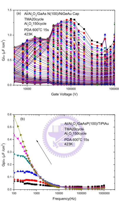
Fig. 2.2 C-V curve of MOS capacitor (a) 500 ℃, 30s (b)600 ℃, 15s
-3 -2 -1 0 1 0.1 0.2 0.3 0.4 0.5 0.6 0.7 C a p a ci ta n ce ( F /cm 2 ) Gate Voltage (V) 1M 100K 10K 1K HK PDA 500oC 30s (a) -3 -2 -1 0 1 0.1 0.2 0.3 0.4 0.5 0.6 0.7 C a p a ci ta n ce ( F /cm 2 ) Gate Voltage (V) 1M 100K 10K 1K HK PDA 600oC 15s (b)
30
Fig. 2.2 C-V curve of MOS GaAs capacitor (c) 600 ℃, 30s (d)700 ℃, 30s
-3 -2 -1 0 1 0.1 0.2 0.3 0.4 0.5 0.6 0.7 C a p a ci ta n ce ( F /cm 2 ) Gate Voltage (V) 1M 100K 10K 1K HK PDA 700oC 30s (d) -3 -2 -1 0 1 0.1 0.2 0.3 0.4 0.5 0.6 0.7 C a p a ci ta n ce ( F /cm 2 ) Gate Voltage (V) 1M 100K 10K 1K HK PDA 600oC 30s (c)
31
Fig. 2.3 C-V curve of MOS GaAs(100) capacitor (a) n-type (b) p-type
-2 -1 0 1 2 3 4 0.15 0.20 0.25 0.30 0.35 0.40 0.45
Al/Al2O3/GaAs N(100)/NiGeAu Cap TMA20cycle Al2O3150cycle C( F /cm 2 ) Gate Voltage (V) 1KHz 10KHz 100KHz (a) -4 -3 -2 -1 0 1 2 0.10 0.15 0.20 0.25 0.30 0.35 0.40 0.45 C( F /cm 2 ) Gate Voltage (V) 100KHz 10KHz 1KHz Al/Al2O3/GaAs P(100)/NiGeAu Cap TMA20cycle
Al2O3150cycle (b)
32
Fig. 2.4 C-V curve of MOS GaAs(111)A capacitor (a) n-type (b) p-type
-3 -2 -1 0 1 2 3 0.0 0.1 0.2 0.3 0.4 0.5 0.6 0.7 0.8 C a p a ci ta n ce ( F /cm 2 ) Gate Voltage (V) (a)
Al/Al2O3/GaAs P(111)A/NiGeAu Cap
preTMA20cycle Al2O380cycle PDA 600oC 15s 300K -3 -2 -1 0 1 2 3 0.1 0.2 0.3 0.4 0.5 0.6 0.7 0.8 C a p a ci ta n ce ( F /cm 2 ) Gate Voltage (V) (b) Al/Al
2O3/GaAs P(111)A/TiPtAu Cap
preTMA20cycle
Al2O380cycle
PDA 600oC 15s
33
Fig. 2.5 QSC-V curve of MOS GaAs capacitor (a) (100) (b) (111)A
-3 -2 -1 0 1 2 3 0.1 0.2 0.3 0.4 0.5 C a p a ci ta n ce ( F /cm 2 ) Voltage (V) 1KHz 10KHz 100KHz QSCV P(100) GaAs (c) -3 -2 -1 0 1 2 3 0.1 0.2 0.3 0.4 0.5 C a p a ci ta n ce ( F /cm 2 ) Voltage (V) 1KHz 10KHz 100KHz QSCV P(111)A GaAs (b)
34
Fig. 2.6 surface potentialψs versus gate voltage VG (a) (100) (b) (111)A
-2 -1 0 1 2 3 4 -0.4 -0.2 0.0 0.2 0.4 0.6 0.8 1.0 1.2 1.4 Su rf a ce p o te n tia l, s (e V) V G-VFB (V) C P(100) GaAs Ei Ec EV (a) -2 -1 0 1 2 3 4 5 -0.4 -0.2 0.0 0.2 0.4 0.6 0.8 1.0 1.2 1.4 P(111)A GaAs Su rf a ce p o te n tia l, s (e V) VG-VFB (V) E Ec EV Ei (b)