準分子雷射低溫製備之鈦酸鍶鉛薄膜元件特性分析之研究
200
0
0
全文
(2) 準分子雷射低溫製備之鈦酸鍶鉛薄膜元件特性分析之研究 Study on the Characterization of Devices with Perovskite Lead-Strontium-Titanate Thin Films Fabricated by Excimer Laser Deposition at Low-Temperatures. 研 究 生: 王志良 指導教授: 鄭晃忠. 國. Student: Jyh-Liang Wang 博士. 立. 交. 電子工程學系. Advisor: Dr. Huang-Chung Cheng. 通. 大. 學. 電子研究所. 博 士 論 文. A Dissertation Submitted to Department of Electronics Engineering & Institute of Electronics College of Electrical & Computer Engineering National Chiao Tung University in partial Fulfillment of the Requirements for the Degree of Doctor of Philosophy in Electronics Engineering February 2007 Hsinchu, Taiwan, Republic of China. 中華民國 九十六 年 二 月.
(3) 推 薦 函. 中華民國九十六年一月三日. 事由 : 推薦電子研究所博士班研究生王志良提出論文並參加國立交通大學博士論 文口試。 說明 : 本校電子研究所博士班研究生王志先生,業已修畢部訂所需學分,通過電子 研究所博士資格考之學科考試,並完成博士論文初稿之撰寫,論文名稱為: 『準 分子雷射低溫製備之鈦酸鍶鉛薄膜元件特性分析之研究』 ,並已有數篇相關之 期刊論文、會議論文及專利發表或送審,茲列舉如下:. 1.. “Polarization Degradation and Breakdown of Pulse-Laser-Deposited (Pb,Sr)TiO3 Films at Low Temperatures”, Jpn. J. Appl. Phys., vol. 46, pp. 267-271, 2007.. 2.. “Characteristics of Low-temperature Pulse-Laser-Deposited (Pb,Sr)TiO3 Films in Metal/Ferroelectric/Silicon Structure”, J. Phys. D: Appl. Phys., vol. 40, pp.254-259, 2006.. 3.. “Study on Fatigue and Breakdown Properties of Pt/(Pb,Sr)TiO3/Pt Capacitors”, J. Phys.: Condens. Matter, vol. 18, pp. 10457-10467, 2006.. 4.. “Structural and Electrical Investigations of Pulse-Laser-Deposited (Pb,Sr)TiO3 Films at Various Oxygen Partial Pressures”, revised to J. Electrochem. Soc... 5.. “Ferroelectric. Characteristics. of. Pulse-Laser-Deposited. Pt/(Pb,Sr)TiO3/Pt. Capacitors at Low Temperatures”, submitted to J. Phys.: Condens. Matter. 6.. “Characteristics of (Pb, Sr)TiO3 Films Post Treated by Low Temperature Technologies”, Electrochemical Society Proceedings, vol. 22, Physics and Technology of High-k Gate Dielectrics II, pp. 469-478, 2003. (SCI). 7.. “A Study of PTC Behavior of (Pb,Sr)TiO3 Thin Films Deposited by Novel Low Temperature Laser Technology”, Proceedings of the 2004 International Electron Devices and Materials Symposia (IEDMS), Hsinchu ROC, pp. 197-200, December 20-23, 2004.. 8.. “Characterization. of. Pulsed-Laser. Low-Temperature. Processing. Deposition. Parameters”,. 10th. (Pb,Sr)TiO3 European. Ferroelectricity 2003, Cambridge UK, pp. 354, August 3-8, 2003.. Films Meeting. with on.
(4) 9.. “The Effect of Post Oxygen Treatment on Pt/(Ba,Sr)TiO3/Pt Capacitors at Low Substrate Temperatures”, IFFF 2002, Nara Japan., pp. 161, May 28-June 1, 2002.. 10.. “鐵電元件之製造方法及鐵電材料之熱處理方法”, 中華民國專利, No. I247045。. 11.. “一種超低漏電流與高熱穩定性之新型鐵電薄膜電容器”, 中華民國專利申請中。. 此外,尚有數篇論文投稿中,準備發表於學術期刊。王志良先生已具備交通大學 電子研究所應有之教育及訓練水準,因此推薦參加國立交通大學電子研究所博士論 文畢業口試。. 此致 國立交通大學電子研究所. 國立交通大學電子研究所教授 ________________ 鄭 晃. 忠 博士.
(5) 準分子雷射低溫製備之鈦酸鍶鉛薄膜元件特性分析之研究. 研究生 : 王志良. 指導教授: 鄭晃忠 博士. 國立交通大學電子工程學系暨電子研究所. 摘 要 本論文將研究以先進低溫製程技術製備之鈦酸鍶鉛((Pb,Sr)TiO3, PbSrT)薄 膜之電容特性,採用的低溫製程技術包含先進低熱預算退火製程及低溫沉積製程 等。本研究中,Pt/PSrT/Pt與Pt/PSrT/Si多層膜結構分別被應用於模擬capacitor over bit line (COB) 結 構 及 鐵 電 閘 場 效 電 晶 體 中 的. 金屬/鐵電/半導. (metal/ferroelectric/semiconductor, MFS)結構。 以雷射剝鍍法(PLD)在低溫(200 oC)所沉積的鈦酸鍶鉛薄膜為非結晶態,具有 極差的鐵電特性,因此需要後續處理以改善電氣特性。傳統的快速退火製程(RTA) 可輕易增進鈦酸鍶鉛薄膜的結晶性,但同時亦因表面缺陷(如:微孔洞)及界面擴 算導致急遽惡化的漏電流。準分子雷射退火(ELA)可在局部區域達到高溫而不損 傷下層結構,因此可用於增進鈦酸鍶鉛薄膜的結晶性。鈦酸鍶鉛薄膜經由準分子 雷射退火後,可減少薄膜表面氧缺乏,並在薄膜上層區域有較佳的結晶性。然而, 準分子雷射退火之效用僅作用於薄膜表層形成”淺層加熱”,無法使整層薄膜都能 結晶。而以準分子雷射退火使鈦酸鍶鉛薄膜進行預先產生晶核,然後搭配快速退 火製程促使晶粒成長的二階段雷射輔助退火製程則能同時實現緻密的薄膜表 面、良好的結晶性、可區別的電容–電場(C-E)電滯曲線、較大的介電常數(492) 及壓抑的漏電流。因而,此二階段雷射輔助退火製程能成功製備具有優越的鐵電 特性、較高的崩潰電壓、較長的元件壽命之Pt/PSrT/Pt電容器。 i.
(6) 以雷射剝鍍在低基板溫度(300 – 450 oC)所製備的鈦酸鍶鉛薄膜具有緻密的 薄膜表面、顯著的結晶性及明顯的鐵電特性。適當的沉積溫度有助於減少鈦酸鍶 鉛薄膜的界面能態及陷阱能態,及較小的漏電流,其電流分析顯示Pt/PSrT/Pt電 容 在 低 電 場 時 的 導 電 機 制 主 要 為 Schottky emission (SE) , 在 高 電 場 則 由 Poole–Frenkel emission (PFE)主導,在本文中將以能帶圖分析探討此導電機制。 實驗顯示,以雷射剝鍍製備的鈦酸鍶鉛薄膜,其從優取向結晶結構及陷阱能態隨 著基板溫度而變化,進而影響薄膜電氣特性。因此,鈦酸鍶鉛薄膜的介電常數及 鐵電特性亦深受從優取向影響,所以在350 – 400 oC沉積的鈦酸鍶鉛薄膜顯現強 化的(100)從優取向結晶性與最佳化的鐵電特性。疲勞操作測試顯示當鈦酸鍶鉛 薄膜的沉積溫度高於350 oC時,Pt/PSrT/Pt電容經1010次切換操作後,僅損失低於 17%的殘留極化值。本文中,400 oC製備的鈦酸鍶鉛薄膜顯示強化的結晶性及較 少的缺陷,因此具有最低的漏電流、最佳的崩潰特性,即使經過1010次切換操作 後亦顯現近乎無疲勞的的電流密度–電場特性。 更進一步分析指出,雷射剝鍍低溫製備的鈦酸鍶鉛薄膜其電流密度隨著量測 溫度及外加電場增加而增加。當量測溫度低於150 oC時,鈦酸鍶鉛薄膜可測得穩 定的電流密度及薄膜電阻,換言之,鈦酸鍶鉛薄膜在積體電路元件操作溫度範圍 內具有相當穩定性,可適用於記憶體應用。而當量測溫度為100 – 390 oC,鈦酸 鍶鉛薄膜亦顯現出強烈的負溫度–電阻係數(negative temperature coefficient of resistance, NTCR)特性,此大範圍的薄膜阻值變動,暗示鈦酸鍶鉛薄膜可應用於 熱敏電阻領域。 此外,鈦酸鍶鉛薄膜的從優取向結晶性、微結構以及電氣特性亦可經由調整 雷射剝鍍時氧氣氛壓力參數(50 – 200 mTorr)而改變。當氧氣氛壓力高於100 mTorr時,鈦酸鍶鉛薄膜將從(100)從優取向結晶性轉換成(110)從優取向結晶性。 因此,順電/鐵電轉變及薄膜介電常數亦與從優取向結晶性及氧含量相關而受到 氧氣氛壓力調變之影響。較高的氧氣氛壓力有助於減少鈦酸鍶鉛薄膜中的氧空 缺,使鈦酸鍶鉛薄膜具有較小的漏電流、較高的崩潰電場,進而增加Pt/PSrT/Pt ii.
(7) 電容器的元件壽命。電流分析顯示Pt/PSrT/Pt電容在低電場時的導電機制主要為 Schottky emission,在高電場則由Poole–Frenkel emission主導,但氧氣氛壓力為200 mTorr時,在低/高電場下都將僅由Schottky emission主導。藉由能帶圖分析疲勞 特性,可得知在較低氧氣氛壓力製備的鈦酸鍶鉛薄膜其疲勞特性深受介面能態影 響,相對的,在較高氧氣氛壓力製備的鈦酸鍶鉛薄膜其疲勞特性則由深的陷阱能 態主導,這種差異導因於氧空缺集中在介面或薄膜內。 鈦酸鍶鉛薄膜亦可以雷射剝鍍法低溫(300 – 450 oC)沉積在p型矽晶片上應用 於 金屬/鐵電/半導 結構。實驗結果顯示基板溫度可強烈增進鈦酸鍶鉛薄膜結晶 性及影響其電氣特性,並且在此沉積溫度範圍內亦無發現交互擴散現象存在 鐵 電/半導 (PSrT/Si)介面。300 oC沉積之鈦酸鍶鉛薄膜內將存在負的陷阱電荷,因 此顯現出小的且為逆時針方向的介電場數–電場電滯曲線及正偏移的平帶電壓 (flatband voltage)。隨基板溫度增加,鈦酸鍶鉛薄膜的結晶性顯著改善,因此具 有較小的漏電流、較少的陷阱能態在電極界面、順時針方向的介電場數–電場 ( ε r -E)電滯曲線及較大的記憶窗(memory window)。然而,過高的基板溫度(450 oC) 可能導致較嚴重的的氧化鉛(Pb-O)揮發,產生較多的缺陷及漏電流特性惡化。分 析固定電荷密度(fixed charge density)及平帶電壓偏移,顯示其陷阱能態特性亦與 電氣特性相契合。本研究中,即使經過1010次切換操作後僅導致記憶窗極小的變 動(< 11%),因此可實現良好的耐疲勞特性。總結,透過準分子雷射退火及沉積 技術之整合,可在低溫製備具有良好結晶性、優越電氣特性之鈦酸鍶鉛(PSrT)薄 膜電容元件,進一步與積體電路技術整合後,將成為深具潛力的非揮發性記憶元 件。. iii.
(8) Study on the Characterization of Devices with Perovskite Lead-Strontium-Titanate Thin Films Fabricated by Excimer Laser Deposition at Low-Temperatures. Student : Jyh-Liang Wang. Advisor : Dr. Huang-Chung Cheng. Department of Electronics Engineering & Institute of Electronics College of Electrical & Computer Engineering National Chiao Tung University. Abstract The characteristics of (Pb,Sr)TiO3 (PSrT) films prepared by novel low-temperature techniques, including low-thermal budget annealings and a low temperature deposition, are systematically investigated in this dissertation. The multilayered structures of Pt/PSrT/Pt and Pt/PSrT/Si are proposed to simulate the practical capacitor over a bit-line (COB) and metal/ferroelectric/semiconductor (MFS) configuration of ferroelectric gate FET, respectively. PSrT films pulsed-laser deposited at 200 oC exhibits amorphous crystallinity and worse ferroelectricities, which indeed require a post-treatment to reform electrical properties. Conventional rapid thermal annealing (RTA) can evidently improve the crystallinity of PSrT films but seriously degrade leakage current due to the unwilling surface defects (i.e. pin holes) and interfacial diffusion. An excimer laser annealing (ELA) technique can recognize local-high-temperature heating within short duration without the underlying damage, proposed to enhance the crystallinity of films. After ELA, the decrease of oxygen deficiency and superior crystallinity of the upper region of films can be obtained. However, the effect of ELA is very limited and can’t iv.
(9) crystallize the whole thickness of film. Furthermore, the novel laser-assisted two-step process, the combination of initial crystal seed induced by ELA and the grain growth carried out by subsequent RTA, which can realize the dense surface, well crystallinity, distinct C-E hysteresis loops, large dielectric constant of 492, and inhibited leakage current density all at once. Thus, the superior ferroelectricity, higher breakdown field and longer lifetime of Pt/PSrT/Pt capacitors can be successfully achieved by this laser-assisted two-step process. PLD PSrT films prepared at low substrate temperatures (Ts), ranging from 300 to 450. oC,. behave dense surface, evident crystallinity, and apparent ferroelectric. properties. Films grown at appropriate Ts yield fewer interface states and fewer trapping states, leading to a smaller leakage current. The conduction mechanism is identified as Schottky emission (SE) at low electric fields and as Poole–Frenkel emission (PFE) at high electric fields. The mechanism analysis shows the electrical characteristics strongly rely on the preferred-oriented textures and trapping states, adjusted by the low substrate temperature (Ts ≤ 450 oC) during PLD process. In addition, the dielectric constant and ferroelectricity are associated with the preferred orientation. The enhanced (100) preferred orientation of films deposited at Ts = 350 – 400 oC exhibits optimum ferroelectricity. The loss in remnant polarization and coercive field is found to be less than 17 % after 1010 switching cycles when Ts is higher than 350 oC. Consequently, the 400 oC-deposited PSrT film reveals the lowest leakage current, nearly fatigued-free J-E characteristics after 1010 switching cycles, and the best breakdown property, attributed to the enhanced crystallinity and fewer defects. Moreover, the current density of these low-temperature PLD PSrT films increases as the measurement temperature and applied fields increase. Films show high stability of leakage current and film resistance below 150 oC, which is important v.
(10) and well for memory application during the operation temperature of IC. Films exhibit strong negative temperature coefficient of resistance (NTCR) behavior at temperatures ranging of 100 – 390 oC. The larger resistance range of the PLD PSrT films infers a potential application of thermistor sensor. Besides, the preferred orientation, microstructure, and electrical characteristics of PLD PSrT films could be apparently affected by ambient oxygen pressures ( PO2 ), ranging from 50 to 200 mTorr. Films exhibit (100) preferred orientation at lower. PO2 and then transit to (110) preferred orientation above 100 mTorr. The paraelectricity/ferroelectricity transition and dielectric constant of films are associated with the preferred orientation and oxygen concentration at various PO2 . Films deposited at higher PO2 exhibit the longer lifetime, higher breakdown field and smaller leakage current density as a consequence of fewer oxygen vacancies (OVs). Except for the case of films deposited at 200 mTorr, the conduction mechanism is identified as SE/PFE at low/high electric fields. The fatigue properties are dominated by interfacial states at low PO2 and by deep trapping states at high PO2 , which could be ascribed to OVs located at the interfaces and inside PSrT films, respectively. PLD PSrT films on p-type Si were studied at low Ts (300 – 450 oC) for MFS applications. The Ts strongly enhances film crystallinity without significant inter-diffusion at the PSrT/Si interface and affects the electrical properties. As Ts increases, films have smaller leakage currents, fewer trap states at the electrode interfaces, clockwise ε r -E hysteresis loops, and larger memory windows correlated with superior crystallinity. Conversely, 300 oC-deposited films exhibit the small and counterclockwise loop with positive shift of the flatband voltage, attributed to more vi.
(11) negative trap charges within the films. However, the high Ts (450 oC) may produce serious Pb-O volatilization, incurring more defects and leakage degradation. The analyses of fixed charge density and flatband voltage shift reveal the trap status and agree well with the leakage characteristic. The excellent fatigue endurance with small variation of memory windows (< 11%) after 1010 switching is also demonstrated. Concisely, PSrT films can be the most promising candidate for future NVRAM capacitor, since the low-temperature process can be compatible to the IC’s integration.. vii.
(12) 誌. 謝. 僅以此論文獻給我最敬愛的父母-王讚榮先生與周阿有女士,感謝你們多年 來辛苦的養育我,教導我,有了你們持續的支持與付出,讓我得以全心全意投入 學業無後顧之憂,順利完成博士學位,同時也要感謝我的哥哥與姐姐-王志旭先 生和王淑鈞女士,在生活上互相的砥礪扶持及幫忙。 感謝我的論文指導教授鄭晃忠博士,老師在研究及待人處事上的教誨,使我 獲益良多。感謝我的論文口試委員,有了委員們的熱心建議與指導,與不辭辛勞 親臨指教,使論文能更趨於完整。感謝實驗室的學長、同學及學弟們,謝謝你們 不管在實驗或是生活上都能夠給予我支持與關心,使得我的研究能夠順利完成, 其中包含了黃全洲學長、史德智學長、李國暥學長、曾章和學長、林敬偉學長、 阮全平同學、曾懷遠學弟、詹爵魁學弟、郭孟維學弟、蔡春乾學弟、常鼎國學弟、 林高照學弟、廖大傳學弟、林君翰學弟、以及柳耀星學弟,有了你們的相伴與合 作此論文才能順利完成。感謝實驗室前助理-高翠敏小姐、簡秀芳小姐、李瑩姿 小姐、凌碧蓮小姐、以及現任助理-張依婷小姐,在行政事務及庶務上的大力協 助及幫忙。 同時感謝國立交通大學奈米中心及國家奈米元件實驗室提供優良的設備與 研究環境,感謝何惟梅小姐和劉曉玲小姐於行政事務上之幫忙,也感謝林素珠女 士、徐秀鑾女士、陳聯珠女士、陳明麗女士、范秀蘭女士、黃月美女士、以及葉 雙得先生在儀器設備及研究器材上的協助。特別感謝周振嘉教授、邱碧秀教授、 劉思謙博士、以及賴宜生教授在實驗資源的協助及論文發表上的建言與指正。最 後感謝所有曾經幫助過我的親朋好友們,謝謝你們一路上給我的支持與關心,我 才可以完成博士學位,謝謝大家。. viii.
(13) Contents. Abstract (in Chinese)………………………………………………………………………...i Abstract (in English)……………………………………………………………………….iv Acknowledgements………………………………………………………………………viii Contents…………………………………………………………………………………...…ix Table Lists………………………………………………………………………………….xiv Figure Captions……………………...…………………………………………………….xvi. Chapter 1 1-1. Introduction. Overview on Perovskite Ferroelectric Materials………………………………...1 1-1-1. Background of Ferroelectric films……………………………………………..1. 1-1-2. Ferroelectrics Capacitors Applied on Memory………………………………6 A. Architectures of Ferroelectric Memory…………………………..………..6 B. Electrical Characteristics of Ferroelectric Capacitor……………………..9. 1-1-3 1-2. Fabrication Methods of Ferroelectric Thin Films………………………….13. Challenges of Advanced (Pb,Sr)TiO3 (PSrT) Capacitors………………………...……15 1-2-1. Basic Properties and Literatures of PSrT Materials………………………...15. 1-2-2. Challenges of PSrT Capacitors Integrated with CMOS IC Process………17. 1-3. Method of Attack…………………...…………………………………………………..19. 1-4. Motivation….......……………..…………………………….…………………………20. ix.
(14) 1-5. Thesis Organization………………...………………………………………………….23. Chapter 2 2-1. 2-2. Experimental Overview. Background of Excimer Laser………………………………………………………25 2-1-1. General Feature of Excimer Laser……………………………………………25. 2-1-2. Concepts of Pulsed-Laser Deposition (PLD)………………………………..26. 2-1-3. Concepts of Excimer Laser Annealing (ELA)……………………………….28. Experimental Details…..………………………………………………………………29 2-2-1. PSrT Films Post-Treated by Novel Laser-Assisted Annealing……………29. 2-2-2. PSrT Films Prepared by Pulsed-Laser Deposition…………………………33. 2-3. Material Characterization Techniques….…………………………...…………………36. 2-4. Electrical Measurement Techniques………….………………………………………..38. Chapter 3. Studies on (Pb,Sr)TiO3 Films Enhanced by Post-Excimer Laser Annealing (ELA) and Subsequent Rapid Thermal Annealing (RTA). 3-1. Concepts of Post-Annealing on Ferroelectrics…………...…………………………….41. 3-2. Experiments……………………………………………………………………..……..42. 3-3. Effects of Rapid Thermal Annealing (RTA) on PSrT Films………....………………..44. 3-4. Effects of Excimer Laser Annealing (ELA) on PSrT Films………………………...….48 3-4-1. Physical Analysis…………………………………………………………..…..48. x.
(15) 3-4-2. Electrical Analysis……………………………………………………………..55. 3-5 Effects of Laser-assisted Two-Step Annealing on PSrT Films………………...…60 3-5-1. Physical Analysis………………………………………………………………60. 3-5-2. Electrical Analysis………………………………………………………..……65. 3-6 Summary……………………………………………………………………………....69. Chapter 4. Explorations of Pulse-Laser-Deposited (Pb,Sr)TiO3 Films at Low Temperatures. 4-1. Concepts of Low-Temperature PLD PSrT Films………………………………...…….71. 4-2. Experiments…………………………………………………………………………..73. 4-3. Physical Analysis……………………………………………………………….……...75. 4-4. Electrical Analysis……………………………………………………………….…….80. 4-5. Reliability Analysis………………………………………………………………..…...89. 4-6. 4-5-1. Breakdown Properties………………………………………………………...89. 4-5-2. Fatigue Properties ……………………………………………………………..91. Summary…………………………………………………………………………..…...94. Chapter 5. Investigations of Pulse-Laser-Deposited (Pb,Sr)TiO3 Films at Various Ambient Oxygen Pressures. 5-1. Concepts of Ambient Oxygen Influence on PLD PSrT Films…………………………95. xi.
(16) 5-2. Experiments………………………………………………………………………..…..96. 5-3. Physical Analysis……………………………………………………………….……...98. 5-4. Electrical Analysis………………………………………………………………..…..107. 5-5. Reliability Analysis…………………………………………………………………...113. 5-6. 5-5-1. Breakdown Properties……………………………………………………….113. 5-5-2. Fatigue Properties……………………………………………………………113. Summary..…………………………………………………………………………….120. Chapter 6. Temperature-Dependent Properties of Pulse-Laser-Deposited (Pb,Sr)TiO3 Films at Low Temperatures. 6-1. Brief Concept of Temperature Coefficient of Resistance………………….…………..121. 6-2. Experiments………………………………………………………………………..…122. 6-3. Temperature Dependent Properties of Pt/(Pb,Sr)TiO3/Pt Capacitors…………….....123. 6-4. Summary…………………………………………………………………………….130. Chapter 7. Characteristics of Low-temperature Pulse-Laser-Deposited (Pb,Sr)TiO3 Films in Metal/Ferroelectric/Silicon Structure. 7-1. Brief Concept of Metal/Ferroelectric/Silicon (MFS) Structure……………………....132. 7-2. Experiments………………………………………………………………………..…133. 7-3. Physical Analysis………………………………………………………………..……135 xii.
(17) 7-4. Electrical Analysis…………………………………………………………………....138. 7-5. Fatigue Properties………………………………………………………………….....145. 7-6. Summary………………………………………………………………………..…….146. Chapter 8. Summary and Conclusions…………………………………...…147. Chapter 9. Future Prospects………………………………………………......151. References…………………………………………………………........………………….152 Vita Publication List. xiii.
(18) Table Lists. Chapter 1 Table 1-1 Summarized requirements of bottom electrode for stacked PSrT capacitor.. Chapter 2 Table 2-1 Wavelength (λ) of an excimer laser depends on the gas molecules used. Table 2-2 Summarized comparisons of various post-treatment technologies. Table 2-3 The process conditions of PSrT film treated with post-annealings: (a) PLD parameters for as-deposited PSrT film, and (b) post-annealing parameters of ELA and RTA. Table 2-4 The PLD process conditions of PSrT film.. Chapter 4 Table 4-1 Comparisons of ferroelectric characteristics for the PSrT films fabricated from different kinds of substrate material and by various deposition techniques.. Chapter 5 Table 5-1 Summarized characteristics of PLD PSrT films deposited at various ambient oxygen pressures on Pt/SiO2/Si (100) wafers.. Chapter 6 Table 6-1 Summarized texture characteristics and electric properties of PLD PSrT xiv.
(19) films deposited at various substrate temperatures (Ts) on Pt/SiO2/Si (100) wafers. Table 6-2 Curie temperature (Tc), log resistance ratio (log (Rmax/Rmin)), and TCR of PSrT films in this thsis and PSrT bulk ceramics reported in literatures.. xv.
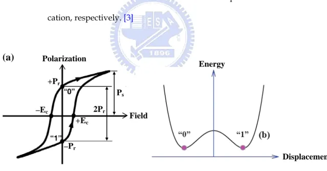
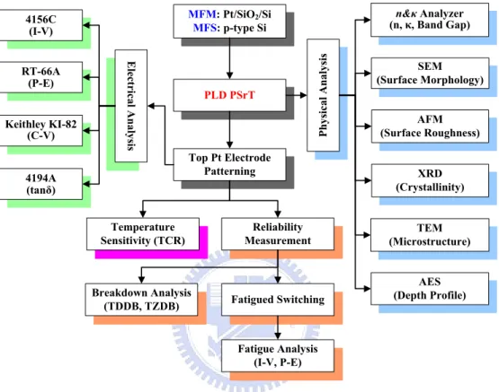
(20) Figures captions. Chapter 1 Figure 1-1 Typical crystal structure of perovskite ABO3, where A is a divalent or or monovalent cation and B is a tetravalent or pentavalent cation, respectively. [3] Figure 1-2 (a) Ferroelectric materials exhibit spontaneous polarization with applied electrical field due to the cation displacement of the body-center ion (B) in the perovskite structure (seen in Fig. 1-1). The saturation polarization, remnant polarization and coercive field are denoted as Ps, Pr and Ec, accordingly. (b) The plot of potential energy versus displacement for ferroelectric material. [1, 3] Figure 1-3 Temperature dependence of the spontaneous polarization and the permittivity in ferroelectric material. (a) – (f) indicate the temperature ranges for each application. [1] Figure 1-4 The relation between permittivity εr and external field E for states of (a) paraelectric phase and (b) ferroelectric phase. [7] Figure 1-5 Applications of ferroelectric films. [3] Figure 1-6 (a) Cell scheme of one-transistor/one-capacitor (1T1C) designed for FeRAM [12]. (b) Schematic stacked structure of typical ferroelectric capacitor over bit-line (COB) [13]. Figure 1-7 Cell scheme of one-transistor (1T) designed for FeRAM. [11] Figure 1-8 Schematic device structure and operation of MFS-FET: (a) on state, and (b) xvi.
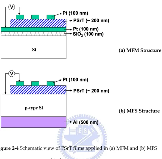
(21) off state. [14] Figure 1-9 Short-time charging and discharging current in Pt/(Ba,Sr)TiO3/Pt, exhibiting power-law behavior for the relaxation current. [15] Figure 1-10 The circuit model of tangent loss due to the leakage current through the loss by a parallel resistance. [7] Figure 1-11 Scheme of different current regimes in metal-insulator-metal systems containing ferroelectric films. [28] Figure 1-12 Phase diagram of PbTiO3–SrTiO3 system. [43] Figure 1-13 Lattice parameters at room temperature as a function of Sr/Pb composition. [45] Figure 1-14 Resistivity-temperature proprieties of PSrT ceramics affected by (a) the composition Sr/Pb ratio [51] and (b) the sintering techniques, such as microwave sintering (ms) and conventional furnace sintering (cs) [52].. Chapter 2 Figure 2-1 Schematic drawings of the practical laser system for (a) PLD mode and (b) ELA mode conducted in this dissertation. Figure 2-2 Schematic view of the multilayer structure conducted for PSrT films post-annealed in this dissertation. Figure 2-3 The experimental flow of PSrT films treated by post-annealing. Figure 2-4 Schematic view of PSrT films applied in (a) MFM and (b) MFS structures in this dissertation.. xvii.
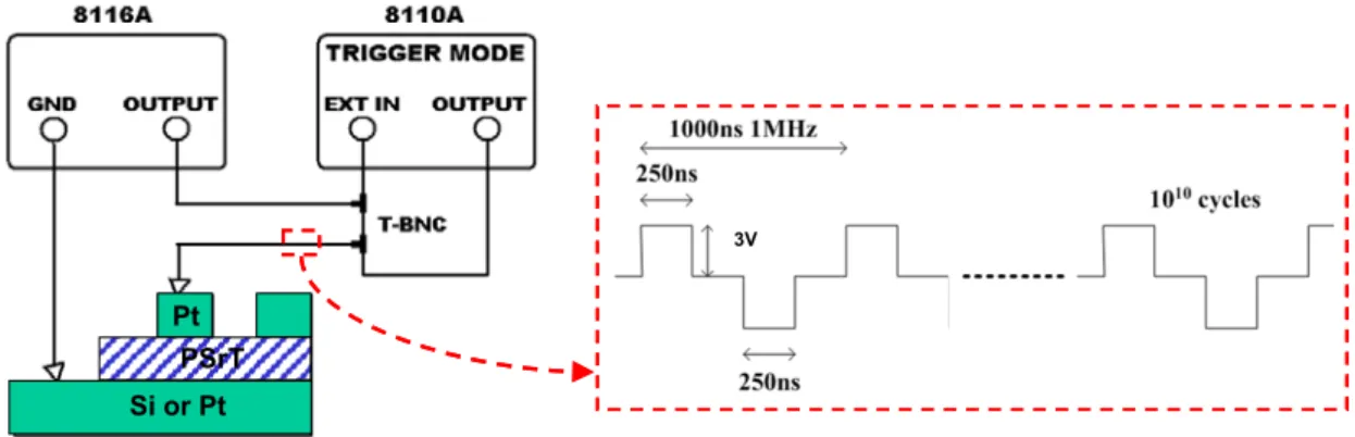
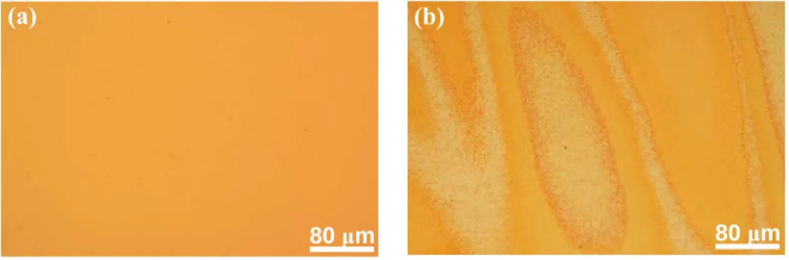
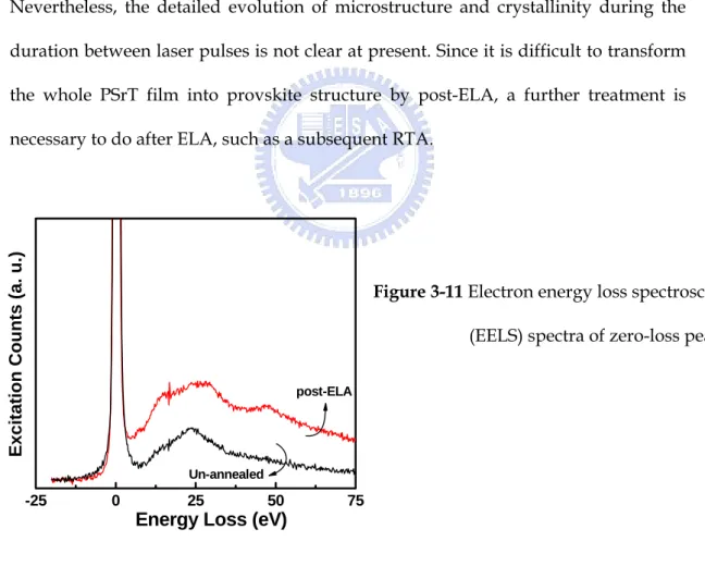
(22) Figure 2-5 The experimental flow of PSrT films fabricated by PLD technique. Figure 2-6 The schematic equipment setup and bipolar switching waveform for the operation of polarization switching degradation (fatigue).. Chapter 3 Figure 3-1 SEM surface morphologies of PLD PSrT films (a) un-annealed and post-rapid thermal annealed (post-RTA) at (b) 450 oC and (c) 600 oC. Figure 3-2 X-ray diffraction pattern of PSrT films un-annealed and post-RTA at 450 and 600 oC. Figure 3-3 Capacitance-electric field (C-E) hysteresis loops of PSrT films un-annealed and post-RTA at 450 and 600 oC. Figure 3-4 Current density versus electric field (J-E) characteristics of PSrT films un-annealed and post-RTA at 450 and 600 oC. Figure 3-5 The reflectivity and the extinction coefficient (κ) of amorphous PLD PSrT thin film for light wavelength from 190 nm to 900 nm. Figure 3-6 Optical microscope surface images of PSrT films (a) un-annealed and (b) post-excimer laser annealed (post-ELA) at laser energy fluence (LEF) of 47.6 mJ/cm2 per pulse with 180 pulses. Figure 3-7 (a)-(d) AFM images and (e) surface roughness of PLD PSrT films un-irradiated and post-excimer laser annealed (post-ELA) with various numbers of laser pulses: (a) un-annealed, (b) 60 pulses, (c) 120 pulses and (d) 180 pulses. Figure 3-8 Relative element ratios (analyzed by ESCA technique) of PSrT films xviii.
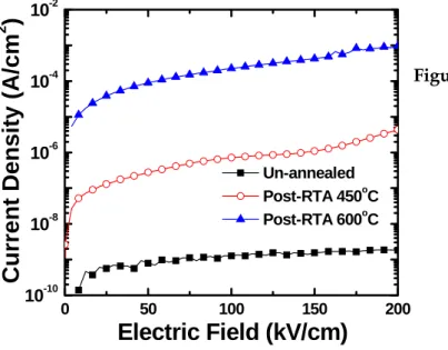
(23) un-annealed and post-ELA with various numbers of laser pulses. Figure 3-9 Glancing incident X-ray diffraction (GIXRD) pattern and the inset conventional XRD pattern for PSrT films un-annealed and post-ELA with various numbers of laser pulses: (a) un-annealed, (b) 60 pulses, (c) 120 pulses and (d) 180 pulses. Figure 3-10 Cross-sectional TEM images and selected–area diffraction patterns (SADPs) of PSrT films un-annealed and post-ELA at LEF of 47.6 mJ/cm2 per pulse with 180 pulses: (a) bright-field (BF) image and SADP of un-annealed, (b) BF image and SADP of post-ELA, (c) minified BF image, (d) minified dark-field of post-ELA (DF) image of post-ELA, (e) enlarged BF image of region A and (f) SADP of region A. Figure 3-11 Electron energy loss spectroscopy (EELS) spectra of zero-loss peak. Figure 3-12 Capacitance-electric field (C-E) hysteresis loops of PSrT films un-annealed and post-ELA with various numbers of laser pulses. Figure 3-13 (a) Current density versus electric field (J-E) characteristics, (b) Schottky emission plot fitting of log (J/T2) versus E1/2, and (c) Poole-Frenkle emission plot fitting of log (J/E) versus E1/2 for PSrT films un-annealed and post-ELA with various numbers of laser pulses. Figure 3-14 Schematic drawings of the electron energy band for PSrT films un-annealed and post-ELA with various numbers of laser pulses. Figure 3-15 SEM surface morphologies of PLD PSrT films (a) post-ELA, and subsequent RTA (post-ELA + RTA) at (b) 450 oC and (c) 600 oC. Figure 3-16 X-ray diffraction pattern of PSrT films un-annealed, post-ELA, and xix.
(24) post-ELA + RTA at 450 oC and 600 oC. Figure 3-17 (a) Cross-sectional TEM image with inset selected-area diffraction patterns (SADPs), and (b) central dark-field (CDF) images of (200)PSrT and (110)PSrT diffraction spots for PSrT films post-ELA + RTA at 600 oC. Figure 3-18 AES depth profiles of PSrT films deposited on Pt/Ti/SiO2/Si substrate: (a) post-ELA and (b) post-ELA + RTA at 600 oC. Figure 3-19 (a) Capacitance-electric field (C-E) hysteresis loops of PSrT films un-annealed, post-ELA, and post-ELA + RTA at 450 and 600 oC. (b) The corresponding dielectric constants of PSrT films un-annealed, post-ELA, post-RTA, and post-ELA + RTA at 450 and 600 oC. Figure 3-20 (a) Current density versus electric field (J-E) characteristics of PSrT films un-annealed, post-ELA, and post-ELA + RTA at 450 and 600 oC. (b) The comparison of leakage current density biased at +100/+150 kV/cm for PSrT films un-annealed, post-ELA, post-RTA at 450 and 600 oC, and post-ELA + RTA at 450 and 600 oC. Figure 3-21 TDDB (time to breakdown as a function of stress field) characteristics of PSrT films post-RTA and post-ELA + RTA at 600 oC.. Chapter 4 Figure 4-1 Deposition rate of PSrT films deposited at various substrate temperatures (Ts) on Pt/SiO2/Si (100) wafers. Figure 4-2 SEM cross-sectional micrograph of PLD PSrT films deposited at Ts = 400 oC. on Pt/SiO2/Si (100) wafers.. xx.
(25) Figure 4-3 SEM surface morphologies of PLD PSrT films deposited at various substrate temperatures (Ts) on Pt/SiO2/Si (100) wafers. Figure 4-4 AES depth profiles of PLD PSrT films deposited on Pt/SiO2/Si (100) wafers at (a) 300 oC, (b) 400 oC, and (c) 450 oC. Figure 4-5 X-ray diffraction analyses of PLD PSrT films deposited at various substrate temperatures on Pt/SiO2/Si (100) wafers: (a) diffraction pattern and (b) texture characteristics. Figure 4-6 (a) Schottky emission (SE) plot fitting of log (J/T2) versus E1/2, and (b) the electron energy band in the interface of substrate electrodes at Ts = 300 oC and Ts ≥ 350 oC. Figure 4-7 (a) Poole-Frenkel emission (PFE) plot fitting of log (J/E) versus E1/2, and (b) the electron energy band inside PSrT films prepared at Ts = 300 oC and Ts ≥ 350 oC. Figure 4-8 Capacitance-electric field (C-E) hysteresis loops of Pt/PSrT/Pt capacitors prepared at various Ts. Figure 4-9 (a) Comparison of saturation polarization (2Ps) and capacitance, and (b) evolutions of remnant polarization (2Pr) and coercive field (2Ec) of Pt/PSrT/Pt capacitors prepared at various substrate temperatures. Figure 4-10 Effect of substrate temperatures on (a) dielectric constant and leakage current density biased at +170 kV/cm, and (b) tangent loss characteristics measured at 100 kHz. Figure 4-11 (a) TZDB field and leakage current density biased at +170 kV/cm, and (b) TDDB characteristics (as a function of electric field) of PSrT films xxi.
(26) deposited at various substrate temperatures. Figure 4-12 (a) Remnant polarization (Pr) vs switching cycles, and (b) normalized degradation of Pr and coercive field (Ec) of PSrT films deposited at various Ts before/after 1010 switching cycles. Figure 4-13 Schottky emission plot fitting of log (J/T2) vs E1/2 for the fresh and fatigued PSrT films prepared at substrate temperatures of 300 and 400 oC.. Chapter 5 Figure 5-1 Deposition rate of PLD PSrT films prepared at various ambient oxygen pressures ( PO2 ) on Pt/SiO2/Si. Figure 5-2 SEM surface morphologies of PLD PSrT films deposited at various ambient oxygen pressures on Pt/SiO2/Si. Figure 5-3 (a) AFM images and (b) surface roughness of PLD PSrT films deposited at various ambient oxygen pressures ( PO2 ) on Pt/SiO2/Si (100) wafers. Figure 5-4 (a) Surface relative element ratios and (b) intensity of oxygen element in AES depth profiles of PSrT films deposited at various ambient oxygen pressures on Pt/SiO2/Si (100) wafers. Figure 5-5 X-ray diffraction analyses of PSrT films deposited at various ambient oxygen pressures on Pt/SiO2/Si (100) wafers: (a) diffraction pattern and (b) texture characteristics. Figure 5-6 Cross-sectional TEM images and selected-area diffraction patterns of PLD. xxii.
(27) PSrT films deposited at (a) PO2 = 100 mTorr and (b) PO2 = 200 mTorr. (c) Grain size in the vertical (V) and horizontal (H) directions of columnar structures. Figure 5-7 (a)-(b) Plane-view TEM images and electron diffraction patterns, and (c)-(d) high-resolution TEM (HRTEM) images and multi-slice image simulations for PSrT films deposited at 50 mTorr and 200 mTorr. Figure 5-8 (a) Capacitance versus electric field (C-E) hysteresis loops and (b) dielectric constant of Pt/PSrT/Pt capacitors prepared at various ambient oxygen pressures. Figure 5-9 (a) Experimental and fitted log (J/T2) versus E1/2 (Schottky emission) plots, and the electron energy band at the interface of substrate electrodes for PSrT films deposited at (b) lower PO2 and (c) higher PO2 . Figure 5-10 (a) Experimental and fitted log (J/E) versus E1/2 (Poole-Frenkel emission) plot, and the electron energy band for PSrT films deposited at (b) lower. PO2 and (c) higher PO2 . Figure 5-11 (a) TZDB (time-zero dielectric breakdown) and (b) TDDB characteristics (time-dependent dielectric breakdown as a function of electric field) of PSrT films deposited at various ambient oxygen pressures. Figure 5-12 The fatigue behaviors of remnant polarization (Pr) versus accumulative switching cycles of Pt/PSrT/Pt capacitors prepared at various PO2 . Figure 5-13 (a) Schottky emission plot fitting of log (J/T2) versus E1/2 and (b) Poole-Frenkle emission plot fitting of log (J/E) versus E1/2 for the fresh xxiii.
(28) and fatigued Pt/PSrT/Pt capacitors prepared at various PO2 . Figure 5-14 Schematic drawings of the electron energy band for the fresh and fatigued Pt/PSrT/Pt capacitors deposited at low and high PO2 .. Chapter 6 Figure 6-1 Current density versus measurement temperature characteristics of Pt/PSrT/Pt capacitors prepared at various temperatures (Ts) as a function of biased field. Figure 6-2 (a) Current density versus electric field curves, (b) resistance-temperature curves, and (c) TCR plots of Pt/PSrT/Pt capacitors prepared at 300 oC. Figure 6-3 Resistance-temperature curves and TCR plots of Pt/PSrT/Pt capacitors prepared at various temperatures (Ts) biased at (a) +50 kV/cm and (b) +150 kV/cm. Figure 6-4 Log resistance ratio, log (Rmax/Rmin), of PSrT films deposited at various substrate temperatures (Ts), where Rmax and Rmin are the maximum and minimum of film resistance measured from 30 to 390 oC.. Chapter 7 Figure 7-1 AES depth profiles of PLD PSrT films deposited on Si (100) wafers at (a) 300 oC and (b) 450 oC. Figure 7-2 (a) X-ray diffraction pattern and (b) texture characteristics of PLD PSrT films deposited on Si at various substrate temperatures. Figure 7-3 Current density versus electric field (log (J)-log (E)) curves of Pt/PSrT/Si xxiv.
(29) capacitors prepared at various substrate temperatures. The corresponding slopes in different regions are denoted as α. Figure 7-4 Experimental and fitted log (J/T2) versus E1/2 (Schottky emission) plots of Pt/PSrT/Si capacitors at (a) positive bias and (b) negative bias. Figure 7-5 Schematic drawing of the electron energy band for the Pt/PSrT/Si structure. Figure 7-6 Hysteresis loops of dielectric constant-electric field ( ε r -E) for the Pt/PSrT/Si capacitors prepared at various substrate temperatures. Figure 7-7 (a) Fixed charge density (Nfc) and leakage current density (at +150 kV/cm) as a function of substrate temperatures for Pt/PSrT/Si structures. (b) Memory window (Vm) of Pt/PSrT/Si capacitors prepared at various Ts. Figure 7-8 ε r -E hysteresis loops of Pt/PSrT/Si capacitors prepared at 450 oC before/after (fresh/fatigued) 1010 fatigued switching cycles.. xxv.
(30) Chapter 1. Introduction. 1-1 Overview on Ferroelectric Perovskite Materials 1-1-1 Background of Ferroelectric films In last three decades, it has brought a marvelous increase in the research of ferroelectric materials in different forms, including single crystals, ceramics, composites, liquids, and thin films [1-8]. A very important group of ferroelectrics is the perovskites, named from the mineral perovskite calcium titanate (CaTiO3). The perfect pervoskite structure (Fig. 1-1) is exteremely simple with the general formula ABO3, where O is oxygen, A represents a cation (a divalent or monovalent metal) with a larger ionic radius, and B is a cation (a tetravalent or pentavalent metal) with a smaller ionic radius. It is cubic, with oxygen ions at the face centers, A ions at the cube corners, and B ions at the body centers. Ferroelectric materials exhibit spontaneous polarization that is reversible with applied electrical field due to the cation displacement of the body-center ion (B) in the structure of perovskite ABO3 crystal as shown in Fig. 1-2(a). The displacement vector D is observed along c-axis and be expressed as. D = ε 0 E + P = ε 0 E + χ eε 0 E = ε 0 ε r E ,. (1-1). ε r = 1+ χe , where E is external electrical field, P is polarization, ε 0 is the vacuum permittivity,. ε r is the relative permittivity (dielectric constant), and χ e is the electric susceptibility. Thus, the electrical polarization can be defined as 1.
(31) A B Oxygen c-axis a-axis a-axis Figure 1-1 Typical crystal structure of perovskite ABO3, where A is a divalent or or monovalent cation and B is a tetravalent or pentavalent cation, respectively. [3]. (a). Polarization. Energy. +Pr Ps 2Pr. –Ec +Ec. Field. –Pr Displacement. Figure 1-2 (a) Ferroelectric materials exhibit spontaneous polarization with applied electrical field due to the cation displacement of the body-center ion (B) in the perovskite structure (seen in Fig. 1-1). The saturation polarization, remnant polarization and coercive field are denoted as Ps, Pr and Ec, accordingly. (b) The plot of potential energy versus displacement for ferroelectric material. [1, 3] 2.
(32) P = ∑ ε 0 ( ε r − 1 )E ,. (1-2). N. Figure 1-2(b) gives the plot of potential energy versus displacement for ferroelectric material, suggesting that the polarization-voltage curve has two stable states (“0” and “1”) at zero voltage after the removal of the field. Ferroelectrics are prime candidates for nonvolatile digital memory devices, since their bi-stable polarization offers the potential for binary memory, which can remain stable after removal of electrical power. In principle, the phenomenon of spontaneous polarization can be analyzed by the energy equation [1].. [(. )(. )]. [. ]. Wtot = Wdip + Welas = k/ 2 Nq 2 - Nαγ 2 / 9ε 0 P 2 + k' / 4 N 3q 4 P 4 , 2. (1-3). where Wtot , Wdip and Welas are the total energy of unit volume, energy of dipole moment and energy of elasticity, respectively. Here, γ is called Lorentz Factor, α is ionic polarizability, N is dipole density, k and k’ are force constant. Spontaneous polarization can occur more easily in perovskite structure due to a high value of Lorenz factor ( γ = 102). Besides, the polarizability of the perovskite ferroelectric material is usually sensitive to temperature, inducing the phase transition. According to the Eq. (1-3), it supposes that the polarizability increases as temperature decreases, so a high α. will result in ferroelectric phase, i.e.. (k/ 2 Nq )- (Nαγ 2. 2. ). / 9ε 0 < 0 . 2. Oppositely, the temperature increasing will lead to paraelectric phase, i.e.. (k/ 2 Nq )- (Nαγ 2. 2. ). / 9ε 0 > 0 . Considering a first approximation of Eq. (1-3), the 2. well-know Currie-Weiss law is derived in paraelectric phase.. 3.
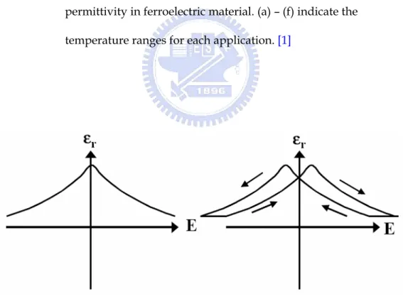
(33) Figure 1-3 Temperature dependence of the spontaneous polarization and the permittivity in ferroelectric material. (a) – (f) indicate the temperature ranges for each application. [1]. (b) Ferroelectric Phase. (a) Paraelectric Phase. Figure 1-4 The relation between permittivity εr and external field E for states of (a) paraelectric phase and (b) ferroelectric phase. [7]. 4.
(34) ε = C(T - T0 ) ,. (1-4). where C is the Currie-Weiss constant. T0 is the Currie-Weiss temperature and slightly lower than the exact transition temperature Tc. While T = Tc, the phase transition occurs and the spontaneous polarization is continuously tending to zero. Figure 1-3 schematically shows the temperature dependence of the spontaneous polarization Ps and permittivity ε r . Ps deceases as temperature increases and vanishes at Currie Temperature. The permittivity follows the Currie-Weiss law in paraelectric phase. The temperature ranges of each application of perovskite ferroelectric material are also denoted in the Fig. 1-3. The material in paraelectric phase, above Tc, is very promising for DRAM capacitor, and that in ferroelectric phase can be applied on nonvolatile memory. Figure 1-4 reveals the relation between permittivity ε r and external field E for states of paraelectric phase and ferroelectric phase. Moreover, a large temperature dependence of the spontaneous polarization occurs below and near the Currie temperature, so the ferroelectric ceramic in this region is suitable for the pyroelectric sensors. These perovskite ferroelectric also possesses properties of piezoelectricity, pyroelectricity, electro-optical effect and acousto-optical effect [1-5].. Figure 1-5 Applications of ferroelectric films. [3]. 5.
(35) Hence, perovskite ferroelectric films can be widely applied on various electronic devices as shown in Fig. 1-5. In this dissertation, we will introduce the application of ferroelectric memory, as well as the nonvolatile random access memory (NVRAM) consisted of pervoskite (Pb,Sr)TiO3 (PSrT) films.. Memory Cell (b) Stacked COB. (a) 1T/1C. Figure 1-6 (a) Cell scheme of one-transistor/one-capacitor (1T1C) designed for FeRAM [12]. (b) Schematic stacked structure of typical ferroelectric capacitor over bit-line (COB) [13].. 1-1-2 Ferroelectrics Capacitors Applied on Memory A. Architectures of Ferroelectric Memory Intensive research is taking place worldwide to develop a large-capacity, high-speed non-volatile memory to replace the dynamic random access memory (DRAM). A ferroelectric random access memory (FeRAM) using a ferroelectric is already mass-produced and available on the market, albeit on a small scale. As can be seen in Fig. 1-6(a), one bit of this FeRAM consists of a transistor and a capacitor. 6.
(36) (1T1C) [11-13], which is the most commonly used. The word line (WL) and bit line (BL) are connected to the gate and drain of the transistor, accordingly. This cell is similar to a DRAM cell with the exception of the plate line (PL) which has a variable voltage level to enable the switching of the polarization of the ferroelectric capacitor, whereas its level is fixed in a DRAM. To write a “1” in the cell, the BL is set to VDD and the PL is grounded, then a pulse is applied at the WL to activate the cell transistor. Writing a “0” is accomplished in the same manner but this time the polarities of BL and PL are exchanged to reverse the polarization of the ferroelectric capacitor [11]. After the power supply is turned off, the ferroelectric capacitor can keep the digital state (“0” and “1”) due to the storage of polarization (Fig. 1-2). The major difference between 1T1C FeRAM and DRAM is nonvolatile datum storage or not. Figure 1-6(b) shows the implementation of 1T1C FeRAM in a stacked structure of capacitor over bit line (COB) [8, 13], which can increase the polarization due to the capability of larger capacitor area [8].. Figure 1-7 Cell scheme of one-transistor. Memory Cell. (1T) designed for FeRAM. [11]. Figure 1-7 presents another cell architecture consisted of a transistor, 1T FeRAM, which uses a ferroelectric film instead of the gate insulating film of the single field-effect transistor (FET) [10, 11]. Among several kinds of ferroelectric gate FET structures, a metal/ferroelectric/semiconductor (MFS) configuration is particularly promising due to the advantages of simple fabrication processes, low power consumption (without the voltage drop across the buffer insulator) and small memory cell size compared to its alternatives. The area required for a single cell is 7.
(37) merely the space occupied by the transistor. MFS-FET exploits the ferroelectric field effect, which is the modulation of conductivity by the electrostatic charges induced by ferroelectric polarization, and thus requires the direct deposition of ferroelectric thin films on silicon (Si) wafer. In this memory, the semiconductor surface conductor channel opens and closes after positive/negative voltage applied on the ferroelectric gate in response to the on/off status of FET, which dependents on the electric polarization stored by the ferroelectric film as shown in Fig. 1-8 [14]. The data memory status is read out as a function of the presence or almost absence of a flowing electric current when a voltage is applied between the drain and source electrodes on both ends of the conductor channel. An advantage of this cell type is that the reading operation does not reverse the ferroelectric polarization and the data is not destroyed (nondestructive read-out, NDRO). This structure is simple and its area is small. In this manner, the 1T FeRAM holds great promise as the ultimate semiconductor memory capable of further miniaturization (higher integration). However, there have still been the technical difficulties of achieving both a high-quality semiconductor surface and a high-quality ferroelectric, incurring the high leakage. The most important problem to be solved has been the short data retention time due to the leaky interface [10, 11].. +Vg. Metal Electrode. -Vg. Ferroelectric. (a) On State. (b) Off State. Figure 1-8 Schematic device structure and operation of MFS-FET: (a) on state, and (b) off state. [14] 8.
(38) B. Electrical Characteristics of Ferroelectric Capacitor Leakage current and power consumption are the critical concerns of the electrical properties applied on the memory capacitor. The conduction mechanisms of high dielectric constant or ferroelectric materials are complicated, which may be associated with dielectric itself, grain boundaries, interfacial layers, electrodes, etc. Besides, many high dielectric constant or ferroelectric materials are found to polarize in a manner that displays substantial time dependence. In addition to an essentially instantaneous or very high-frequency polarization, polarization charging current flow into such materials with a power-law time dependence of approximately t-n, where n ≤ 1 usually, as shown in Fig. 1-9 [15]. The charging current is the sum of the polarizing current, which dominates at short times because of its t-n behavior, and the true leakage current is referred to the current flow from electrons or holes, which dominates at long time. Therefore it should be very careful to identify the real and steady leakage current from the polarizing current with including a proper delay time during the I-V measurements. The leakage behaviors of the ferroelectric material can be expressed by several conductive models due to many complicated mechanisms coexisted. Usually the Ohmic contact is not easily formed between the high dielectric constant or ferroelectric materials and electrodes, unless the carrier concentration of dielectrics is high enough in the interface and results in tunneling effect. Besides, the ultra-thin dielectric insulator (i.e. thinner than 30 nm) behaves tunneling current. Because there is strong temperature dependence of leakage current in the dielectrics, both Schottky emission (SE) (or thermionic emission) and Poole-Frenkel (PFE) transport are the possible conduction mechanisms [16-18]. The equations of these two conduction mechanisms are shown as the following. { [. ] }. SE : J SE = A*T 2 exp − q ϕ B − ( qE / 4πε d ε 0 )1 / 2 /kT , 9. (1-5).
(39) { [. ] }. PFE : J PF = BEexp − q ϕt − ( qE / πε d ε 0 )1 / 2 /kT ,. (1-6). where A* is the effective Richardson’s constant, φB is the potential barrier height in the interface, B is a constant, φt is the trapped energy level, εd is the dynamic dielectric constant of the ferroelectric material in the infrared region, q is the unit charge, k is Boltzmann’s constant, J is current density, T is absolute temperature, correspondingly .In addition, many researches reported lots of other theories about the leakage current, such as space charge limited current (SCLC) [19-20] and the effect of grain boundaries [21]. Consequently, the conduction mechanisms should be determined by the practical conditions, which is associated with the form of energy band diagram constructed from dielectrics, electrodes, grain boundaries, etc. [21-24].. Figure 1-9 Short-time charging and discharging current in Pt/(Ba,Sr)TiO3/Pt, exhibiting power-law behavior for the relaxation current. [15]. The tangent loss is due to the leakage current through the loss by a parallel resistance shown in Fig. 1-10 [7]. It is defined as the ratio of the leakage current through the resistance (IR) to the leakage current through the ideal dielectric (IC). Therefore the value of tangent loss can be extracted from the following equations: 10.
(40) Q = CV , V = V0 e jωt ,. Z = R + jX = 1 j ωC. I = ∂Q ∂t = jωCV = jωC0 ( ε ′ − jε ′′ )V = jωC0ε ′V + ωC0ε ′′V. = 1 jωC0 ( ε ′ − jε ′′ ) = 1 ωC0 ( ε ′′ + jε ′ ). = IC + I R ,. = ( ε ′ − jε ′′ ) ωC0 ( ε ′′ + jε ′ ), tan δ = ε ′′ ε ′ = R X ,. tan δ = I R I C = ε ′′ ε ′ ,. Figure 1-10 The circuit model of tangent loss due to the leakage current through the loss by a parallel resistance. [7]. Q = CV , V = V0 e jωt , I = ∂Q ∂t = jωCV = jωC0 ( ε ′ − jε ′′ )V = jωC0ε ′V + ωC0ε ′′V = I C + I R ,. (1-7). tan δ = I R I C = ε ′′ ε ′ , where ε = ε '-jε " ,. Z = R + jX = 1 / jωC0 ( ε ' − jε" ) = ( ε" − jε ' ) / ωC0 ( ε" 2 +ε ' 2 ) , ∴ tanδ = ε" /ε ' = R/X ,. (1-8). where C is the capacitance, C0 is the geometric capacitance in free space, Z is impedance, ε’ and ε” are the relative real and imaginary dielectric constants, R and X are series relative real and imaginary impedance (resistance). Usually the tangent loss comes from two mechanisms: resistive loss and relaxation loss. In the resistive loss mechanism, the energy is consumed by mobile charges in the film. In the case of. 11.
(41) the relaxation loss mechanism, it is the relaxation of the dipole that expends the energy. Both two mechanisms of tangent loss are associated with the leakage current in the ferroelectric films, also investigated in this dissertation. For the paraelectric or ferroelectric dielectrics, there are many electrical properties that will change with time, including the dielectric constant, remnant and saturation polarization, coercive field, tangent loss, leakage current, breakdown field, etc. Three time-dependent mechanisms will affect these electrical properties, which are aging, fatigue and resistive degradation. Aging is generally defined as a spontaneous change in electrical properties with time, either under electrical stress or not. Fatigue is related to the ability decrease to switch the memory cell into the opposite state, after being kept programmed in one state for long periods of time. This effect is related to the polarization decrease in the hysteresis loop and it is proportional with the increasing number of switching cycles. Both mechanisms are found in ferroelectric states and believed due to the pinning of domain walls from charge trapping, oxygen vacancies and associated defect dipoles [2, 25-27].. Figure 1-11 Scheme of different current regimes in metal-insulator-metal systems containing ferroelectric films. [28]. 12.
(42) The third mechanism is time-dependent dielectric breakdown (TDDB), which is also referred as resistance degradation, for both paraelectric and ferroelectric dielectrics. It is defined as an increase of the leakage current under a constant applied electric field after prolonged times, also shown in Fig. 1-11 [28]. In this dissertation, the mechanisms of leakage, fatigue and TDDB for (Pb,Sr)TiO3 (PSrT) films were methodically addressed.. 1-1-3 Fabrication Methods of Ferroelectric Thin Films Experientially, fabrication methods of perovskite thin films can be categorized into three types, such as chemical solution deposition (CSD), chemical vapor deposition (CVD) and physical vapor deposition (PVD). 1.. Chemical solution deposition (CSD) The dielectric and ferroelectric films can be deposited by spin coating in CSD technique such as sol-gel [3, 22-24] and metal-organic deposition (MOD) [3]. Easy process, low cost, high throughput and simple facility requirement are the advantages of CSD technique. Although there are many advantages for CSD technologies, numerous problems still exist in this technology, such as the contamination control in the solvent and the porosity after baking. Besides, poor control of the perovskite phase stoichiometry can stem from varieties of the chemical source conditions. Poor step coverage and film crack after annealing are another problems.. 2. Chemical vapor deposition (CVD) The CVD technology, such as metal-organic chemical vapor deposition (MOCVD) [29, 30], liquid source misted chemical vapor deposition (LSMCVD) [3, 4], etc., can fabricate ferroelectric film for high-density devices due to excellent step coverage and uniformity. However, more complicated 13.
(43) mechanisms of CVD process results in difficult process control, and the high temperature post-treatments are needed for removing the carbon species from precursor. Besides, the process temperature of CVD is still very high for CMOS technology because of the chemical reaction requirement. Also utilizing metal-organic precursors, with which the technique is so called MOCVD, reduces the process temperature. However, more complicated mechanisms of the process are resulted and the remove of carbon species from precursors is needed with post-treatments (curing and annealing). Besides, LSMCD is one of CVD methods to deposit dielectrics. Only single precursor is misted by atomizer, carried to a chamber by Ar carrier gas and deposited on a substrate. The drying (baking and curing) and high-temperature crystallization (annealing) processes are also needed. However, the uniformity for run to run is not stable. 3. Physical vapor deposition (PVD) The PVD technique includes sputtering [3, 6-8], pulsed-laser deposition (PLD) [3, 31] … etc. Sputtering is a term used to describe the technology in which atoms are removed from the target surface by collision with high energy particles. Sputtering can afford to perform a uniform thickness using large area target. Besides, sputtering is a low cost, mature and easy-controlled technique. However, poor step coverage and different sputtering yield for different elements are disadvantages of sputtering. PLD can easily achieve a wide variety of stoichiometry of ferroelectric film, which is simple, versatile, and capable of epitaxy growth and excellent crystallinity without subsequent high-temperature annealing. In this dissertation, the excmier pulsed-laser deposition technique was applied on the fabrication of PSrT film.. 14.
(44) Mostly, ferroelectric thin films require low-temperature processes for IC and MEMS applications to prevent the formerly-fabricated structure from thermal damage. The high-temperature process will result in the volatilization of Pb-O in lead-titanate-based films, the loss of Bi content in bismuth-tatanate-based films, the diffusion of constituent elements and/or the chemical reactions between ferroelectric film and underlying layer, which in turn affects the film composition and degrades the electric properties of ferroelectric device [3, 4, 8]. Thus, a low-thermal budget process, a relatively low-temperature process with short thermal-duration, is certainly required for the preparation of PSrT thin films.. 1-2 Challenges of Advanced (Pb,Sr)TiO3 (PSrT) Capacitors 1-2-1 Basic Properties and Literatures of PSrT Materials PbTiO3 (PTO) film has been considered for applications in nonvolatile random access memory (NVRAM), but many drawbacks of this film must be improved, such as high coercive field, high crystallization temperature, and poor microstructure. Normura and Sawada investigated polycrystalline samples of (Pb,Sr)TiO3 (PSrT) ceramic system and established a complete series of solid solution from PbTiO3 (PTO) to SrTiO3 (STO) since 1955 [41, 42]. STO films have a cubic structure at room temperature and characterized by lower crystallization temperature and lower dielectric constant than those of PTO films [43, 44].. PTO and STO films, at room. temperature, behave a tetragonal structure (ferroelectric phase) and a cubic structure (paraelectric phase), respectively, because PTO has the Curie temperature (Tc) at 490 oC. and STO has the Tc at -220 oC. The Tc can be linearly adjusted from -220 oC to 490. oC. by varying the lead (Pb) content in the PSrT ceramics as indicated in Fig. 1-12 [42].. It is reported that PTO forms continuous range of solid solution with STO, the lattice 15.
(45) volume and the tetragonality (c/a, the ratio of c-axis/a-axis lattice constant) of PTO decrease with the increment of Sr/Pb composition ratio [44-47], presented in Fig. 1-13. The effects of lead substituted by strontium (Sr) in the PTO film decrease the crystallization temperature and offer a good control of the dielectric properties at room temperature [47, 48].. Figure 1-12 Phase diagram of PbTiO3–SrTiO3 system. [42]. Figure 1-13 Lattice parameters at room temperature as a function of Sr/Pb composition. [45]. Moreover, PSrT have aroused considerable interest in the composite effect of negative and positive TCR (NTCR and PTCR), firstly found in 1988 [49]. In the past studies [50-55], PSrT ceramics are found to exhibit a NTCR behavior below Tc and the PTCR effect above Tc. Figure 1-14 indicates that the resistivity-temperature 16.
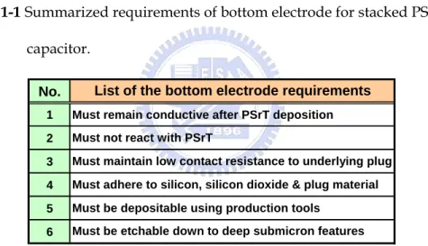
(46) properties of PSrT ceramics are functions of the composition Sr/Pb ratio and also affected by the fabrication process, such as the different sintering techniques. Therefore, PSrT is suitable for memory, sensor, frequency tuning devices and microwave applications due to its large electric-field-dependent dielectric constant and composition-dependent Curie temperature [42-60].. (a). (b). Figure 1-14 Resistivity-temperature proprieties of PSrT ceramics affected by (a) the composition Sr/Pb ratio [51] and (b) the sintering techniques, such as microwave sintering (ms) and conventional furnace sintering (cs) [50].. 1-2-2 Challenges of PSrT Capacitors Integrated with CMOS IC Process PSrT is the superior candidate material of future NVRAM, but there are still some challenges for the integrations of CMOS process. 1.. CMOS devices deformed by high temperature process In general, high deposition temperature (> 550 oC) of PSrT films is frequently 17.
(47) applied to obtain good crystallinity of a perovskite structure [42, 47, 56-60], but the high temperature process may deform the junction profile and alter the gate length of the metal-oxide-semiconductor (MOS) FET, especially on the deep submicron scale. In stacked-capacitor structure, the dopant of MOS-FET is always implemented prior to the capacitor fabricated, which needs to be fabricated at low temperature to avoid the damage of the MOS-FET. 2.. Suitable bottom electrode formation of PSrT capacitor Usually, there is serious reaction or inter-diffusion between ferroelectric and bottom electrode during the deposition processing at high temperature. A thermally and electrically stable bottom electrode is indeed required for ferroelectric capacitor prepared at relatively low-temperature. Here, Table 1-1 lists down the most significant requirements of bottom electrode for stacked PSrT capacitor.. 3.. Dramatic variations of the electrical properties for the device operating in various temperatures As mentioned, PSrT exhibits strong TCR properties, especially when temperature approaches Tc. It means that the electrical properties of PSrT, i.e. leakage current, can dramatically change with temperature. Thus, the Tc of PSrT is necessary to be much higher than the temperature of memory operation. In general, the operation junction-temperatures for consumer IC applications and is designed lower than 125 oC and qualification spec ranges from –0 oC to +120 oC (ambient temperature ranging of –40 – +120 oC). In this dissertation, the TCR properties of PSrT are performed to sure if the normal device operation can be obtained at ≥ 120 oC.. 4.. Unwilling interface properties between PSrT and silicon due to high temperature process 18.
(48) The high-temperature process will cause the diffusion of constituent elements and/or the chemical reactions between ferroelectric film and underlying silicon, which produce undesirably high density of interfacial trap states. Thus, a leaky interface and high leakage current will appear and destroy device characteristics of MFS-FET. A low-temperature technique is the key for the using of PSrT in 1T FeRAM. Therefore, the thin film technologies of the PSrT capacitors must overcome the above tough blockade, or it should be impossible to achieve the practical NVRAM applications.. Table 1-1 Summarized requirements of bottom electrode for stacked PSrT capacitor. List of the bottom electrode requirements. No. 1. Must remain conductive after PSrT deposition. 2. Must not react with PSrT. 3. Must maintain low contact resistance to underlying plug. 4. Must adhere to silicon, silicon dioxide & plug material. 5. Must be depositable using production tools. 6. Must be etchable down to deep submicron features. 1-3 Method of Attack It is clear that the low-temperature preparing techniques are necessary for PSrT films applied on memory. Furthermore, the noble metal platinum (Pt), with low resistivity, is considered as the electrode material because of its low power consumption and RC delay, and good stability to lead-based perovskite materials [4, 57]. In dissertation, we perform two approaches for this goal expressed as following. 19.
(49) 1.. PSrT films post-treated by novel laser-assisted annealing A low-thermal budget treatment, laser-assisted annealing, is proposed to improve the poor crystallinity of PSrT films deposited at extremely low temperature. The multi-layer structure of Pt/PSrT/Pt/Ti/SiO2/p-type Si was used in this work. The specific parameters of PSrT film preparation and post-annealings were carefully controlled. The thinner (~ 120 nm) PSrT film was adapted due to the limited depth of laser absorption in ferroelectrics. The novel laser-assisted two-step process, the combination of initial crystal seed induced by ELA and the grain growth carried out by subsequent RTA, which may be a potential technique to improve the crystallinity and electrical properties of PSrT films and systematically investigated in this dissertation.. 2.. PSrT films prepared by pulsed-laser deposition A relatively low-temperature (≤ 450 oC) pulsed-laser deposition is conducted to prepare PSrT film for two architectures, MFM and MFS, which are used to simulate the devices of COB and MFS-FET, accordingly. The process parameters were seriously controlled, and the material characterizations and electrical properties were scientifically conducted to obtain the optimal process conditions. The corresponding mechanisms were also thoroughly studied in this dissertation.. 1-4 Motivation This dissertation dedicated in obtaining excellent characteristics of PSrT capacitor fabricated by novel low-temperature technologies. The motivation and the major concepts of this study are listed below. 20.
數據
+7

Outline
Electrical Characteristics of Ferroelectric Capacitor
Experimental Overview
Studies on (Pb,Sr)TiO 3 Films Enhanced by Post-Excimer Laser
Explorations of Pulse-Laser-Deposited (Pb,Sr)TiO 3 Films at
Investigations of Pulse-Laser-Deposited (Pb,Sr)TiO 3 Films at
Temperature-Dependent Properties of Pulse-Laser-Deposited
Characteristics of Low-temperature Pulse-Laser-Deposited
Summary and Conclusions
Future Prospects
相關文件
plotyy 2-D line plots with y-axes on both left and right side loglog Log-log scale plot.. semilogx Semilogarithmic plot semilogy Semilogarithmic plot errorbar Plot error bars
The continuity of learning that is produced by the second type of transfer, transfer of principles, is dependent upon mastery of the structure of the subject matter …in order for a
➢ Plot the learning curves (ROUGE versus training steps)... ➢ What is your final
The stack H ss ξ (C, D; m, e, α) was constructed in section 2.3.. It is a smooth orbifold surface containing a unique orbifold point above each ℘ i,j.. An inverse morphism can
或改變現有輻射源之曝露途徑,從而使人們受到之曝露,或受到曝露
FIGURE 23.22 CONTOUR LINES, CURVES OF CONSTANT ELEVATION.. for a uniform field, a point charge, and an
1. Infall guided by magnetic field, forming flattened envelope 2. Keplerian disk formed in flattened env. feeding protostar 3. Magnetic braking may reduce the disk size, if J
using tungsten single crystal emitters the thermally-assisted Schottky type, using emitters of zirconium oxide. field emission
![TraditionalMLCalgorithmsmainlytacklethebatchMLCproblem,wheretheinputdataarepresentedinabatch[24,28].Nevertheless,inmanyMLCapplicationssuchase-mailcategorization[22],multi-labelexamplesarriveasastream.Onlineanalysisistherefore dimensionreducermotivatedbyma](data:image/gif;base64,R0lGODlhAQABAIAAAP///wAAACH5BAEAAAAALAAAAAABAAEAAAICRAEAOw==)