國
立
交
通
大
學
電子工程系 電子研究所碩士班
碩士 論
文
氮化鈦/氧化鋁鉿/氮化鈦金氧金電容之電性分析
與電壓電容係數物理模型
Electrical Analysis and Physical Model of the
Voltage Coefficient of Capacitance of the
TiN/HfAlO/TiN MIM Capacitors
研 究 生 : 黃勻珮
指 導 教 授 : 崔秉鉞教授
氮化鈦/氧化鋁鉿/氮化鈦金氧金電容之電性分析與電
壓電容係數物理模型
研究生:黃勻珮
指導教授: 崔秉鉞 博士
國立交通大學
電子工程系 電子研究所碩士班
摘要
在本篇論文中,我們採用摻雜鋁金屬之二氧化鉿之高介電材料作為金屬-氧化物-金 屬(MIM)電容的介電質,摻雜兩種比例的鋁金屬,分別為 10%與 14.7%。試片厚度分為 三種:15nm、25nm、35nm。鋁摻雜為 10%且厚度為 15nm 的試片,在 3V 頻率為 1MHz 的量測條件下,得到電容密度約 13.6 fF/μm2,其所對應的介電常數約為 23;而鋁摻雜 為 14%且厚度為 15nm 的試片中,電容密度約為 11.3 fF/μm2而其所對應的介電常數約為 19.5。兩者相比,鋁摻雜濃度越低(即鉿元素含量較高),介電常數較高,所得到的電容 密度也較高。本篇論文之電容密度達到 2013 年 ITRS 的規格。而在改良漏電流方面, 於 1V 的偏壓下,兩種不同鋁摻雜量且厚度皆為 15nm 的試片,其漏電流分別為 1.88×10⁻⁸(A/cm2) 及 1.72×10⁻⁸ (A/cm2)。漏電流機制,於非常低電場下呈現歐姆傳導機制(Ohmic conduction);中等電場下呈現蕭基發射傳導機制(Schottky Emission);高電場則呈現 Frenkel-Poole 傳導機制。
摻雜 14%且厚度 35nm 的試片,其 VCC 僅有 259(ppm/V2 ),然而,造成 VCC 現象之基 本機制目前尚無定論,由已知的實驗結果顯示,VCC 與本身材料種類、薄膜厚度有關。 本篇論文提出一個修改過的物理模型,藉由邊界缺陷電容值與量測頻率和偏壓之間的關 係式,也可經由適當的轉換,成為自矽基底表面的穿隧距離和自氧化鋁鉿之導帶邊緣的 缺陷能階深度。以一穿透梯形位能障礙的彈性直接穿隧物理模型為理論基礎,我們能夠 藉由一平滑的三維網線,來描述在氧化鋁鉿的邊界缺陷之空間與能階分佈。而所萃取之 結果介於 1×10¹⁵ ~3×10¹⁷ (cm-3eV-1)之間,且與 VCC 成正相關。推測此種邊界缺陷是 VCC 的成因之ㄧ。最後,我們也討論了此方法的限制。
Electrical Analysis and Physical Model of the Voltage
Coefficient of Capacitance of the TiN/HfAlO/TiN
MIM Capacitors
Student: Yun-Pei Huang
Advisor: Dr. Bing-Yue Tsui
Department of electronics Engineering and Institute of electronics
National Chiao Tung University
Abstract
In this thesis, we use HfAlO as the dielectric layer in MIM capacitors. HfAlO films with two different Al percentages were deposited. The Al percentages are 10% and 14.7%. The thickness of samples is divided into three kinds of thickness: 15nm, 25nm, and 35nm. The capacitance density is 13.6 fF/μm2 with 10% Al content and the dielectric constant is about 23 at 3V and 1MHz. The capacitance density is 11.3 fF/μm2 with 14.7% Al content and the dielectric constant is about 19.5. The lower Al percentage is (Hf content is higher), the higher capacitance density is. The capacitance density meets the requirement of 2013 ITRS. The leakage current densities of the samples with 15nm-thick HfAlO and 10% and 14.7% Al content are 1.88×10⁻⁸ and 1.72×10⁻⁸ (A/cm2) at 1V bias, respectively. The leakage current
Conduction at moderate electric field, and Frenkel-Poole conduction at high electric field. The lowest parabolic voltage coefficient of capacitance (VCC-) in this thesis is about 259(ppm/V2) with Al content of 14% Al content and thickness of 35nm. A physical model considering the pre-existing border traps was proposed to account for the VCC-. From the frequency and electrode bias voltage dependences the spatial and energy distribution from Si substrate surface and from HfAlOconduction band edge could be extracted, respectively. The orders of the magnitude of the extracted border trap volume densities are around 3×10¹⁷ (cm-3eV-1), which have positive correlation with the VCC-. Increasing the Al content can reduce the trap density and the VCC-. The limitations of detectable space and energy depth of the physical model are also discussed briefly.
誌謝
隨著論文的完成,學生生涯也要劃下句點了。回首這幾年,我首先要感謝我的指導 老師 崔秉鉞教授,老師在論文與研究上的諄諄教誨以及嚴謹認真的專業態度,總讓我 受益匪淺;而老師的熱心公益以及耿直的做人態度更是我學習的典範。 其次感謝工研院電光所提供沉積薄膜的服務,以及交通大學奈米中心和國家奈米研 究實驗室提供我完善的實驗環境。 感謝實驗室的學長姊黃誌鋒、謝志民、盧季霈、李佳蓉、林孟漢、吳明錡、黃永助 在實驗上的討論幫忙與機台的訓練;感謝實驗室的夥伴李振欽、李振銘、洪玉仁同學的 幫忙,還有學弟妹張孝瑜、劉筱函、張嘉文、蔡雨蓁、羅正愷、蔡依成、王俊凱、賴瑞 堯的陪伴以及幫忙約run 以及處理實驗室的事務,讓我可以更專心在實驗上,謝謝你們 大家。 謝謝我的好朋友們 曾禎宇、畫重憲、黃瓊芬、蔡婉清,有你們的聊天與陪伴,美 好的回憶點滴在心,祝福你們。 最重要的感謝我親愛的父母 黃江漢先生、馬錦玉女士,謝謝你們從小的栽培與照 顧,以及男友 鄞毅捷的打氣與鼓勵,使我無後顧之憂得以完成論文。Contents
Abstract (in Chinese) ... i
Abstract (in English)... iii
Acknowledgement ...v
Contents... vi
Figure captions ... viii
Table captions ... 1
Chapter 1 Introduction ... 1
1.1 Historical Perspective
... 1
1.2 Present issue of Mental-Insulator-Metal capacitor
... 2
1.3 Motivation
... 3
1.4 The Organization of This Thesis
... 4
Chapter 2 Experimental Procedure ... 8
2.1 Device Fabrication
... 8
2.2 Material and Electrical Analysis
... 9
Chapter 3 Analysis of HfAlO MIM Capacitor ... 18
3.1 Introduction
... 18
3.2 Material analysis
... 19
3.3 Analysis of Capacitance Dependence on Voltage and Frequency
... 19
3.4 Leakage current mechanism
... 21
3.5 The trap density extracted from the improved physical model
... 24
3.6 Limitation of the modified Physical model
... 27
Chapter 4 Conclusions... 63
4.1 Summary
... 63
4.2 Future works
... 64
Figure captions
Chapter 1 Introdution
Fig. 1- 1 DC bias dependence of normalized capacitance (△C/C0) at 100 k ... 7
Chapter 2 Experimental Procedure
Fig.2-1 Process flow and schematic cross-sectional drawings of the TiN/HfAlO/TiN MIM capacitors. ... 16 Fig.2-2 (a) Typical parallel circuit model in Agilent 4284A (b) Five-element circuit model
proposed by W. H. Wu [2-1]. ... 16 Fig.2-3 Capacitance-voltage curves of the TiN/HfO2/SiO2/n-Si MOS capacitor measured and
corrected at various frequencies [2-1]. ... 17
Chapter 3 Analysis of HfAlO MIM capacitor
Fig. 3-1 The TEM images of TiN/HfAlO/TiN MIM capacitors with(a) Al:Hf=1:8.7,
15nm-thick (b) Al:Hf=1:8.7, 25nm-thick(c) Al:Hf=1:8.7, 35nm-thick (d) Al:Hf=1:5.8, 15nm-thick (e) Al:Hf=1:5.8, 25nm-thick (f) Al:Hf=1:5.8, 35nm-thick. ... 32 Fig. 3- 2 Comparison of the original and the corrected C_F characteristics with (a)-(f)
thickness :15nm, 25nm, 35nm at 3V. ... 36 Fig. 3- 3 VCC-α versus voltage characteristics of Al:Hf=1:8.7 and Al:Hf=1:5.8 with
dielectric thickness :15nm, 25nm, 35nm at 3V. ... 40 Fig. 3- 4 (a)Thickness dependence of VCC-α for the MIM capacitors with Al:Hf=1:8.7. The
inset shows VCC-α dependence on capacitance density (b)Thickness dependence of VCC-α for the MIM capacitors with Al:Hf=1:5.8. The inset shows VCC-α dependence on capacitance density. ... 42 Fig. 3- 5 (a) Typical J-V characteristics of the MIM capacitors with Al:Hf=1:8.7 (b) Typical
J-V characteristic of the MIM capacitors with Al:Hf=1:5.8... 44 Fig. 3- 6 (a) Schottky emission fitting of TiN/HfAlO/TiN capacitors with Al:Hf=1:8.7 (b)
Schottky emission fitting of TiN/HfAlO/TiN capacitors with Al:Hf=1:5.8. ... 45 Fig. 3- 7 Trap-assist tunneling (TAT) model fitting of the TiN/HfAlO/TiN capacitors with
Al:Hf=1:8.7. The slope at the linear region gives a value of 10t -6 eV. This
unreasonable value indicates that the current transport is not dominated by the TAT
mechanism. ………...45 t
Fig. 3-8 (a)-(f) Ohmic conduction fitting of 15nm, 25nm and 35nm-thick TiN/HfAlO/TiN capacitors with Al:Hf=1:8.7 and Al:Hf=1:5.8... 50 Fig. 3-9 (a)-(f) Fenkel-Poole conduction fitting of 15nm, 25nm and 35nm-thick
Fig. 3- 10 The border trap capacitance in parallel with the ideal capacitance ... 54 Fig. 3- 11 Schematic band diagram of the TiN/HfAlO/TiN MIM capacitor biased at top
electrode with illustration of tunneling distance and carrier energy coordinates... 54 Fig. 3- 12 (a)-(f) The space and energy distribution of border trap volume density Nbt
(cm-3eV-1) of all samples at forward and reverse bias... 60 Fig. 3- 13 Capacitance-Voltage characteristics of the TiN/HfAlO/TiN MIM capacitors at
various frequencies... 61 Fig. 3- 14 Schematic band diagram of the TiN/HfAlO/TiN MIM capacitor with high
frequency... 61 Fig. 3- 15 The calculated trap energy depth and tunneling distance with different work
Table captions
Chapter 1 Introdution
Table 1- I The requirement for RF device according to ITRS ... 6 Table 1- II Summarized material and electric properties of several high- κ gate dielectrics
[1-5]. ... 6
Chapter 2 Experimental Procedure
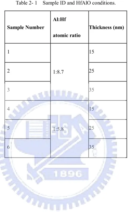
Table 2- 1 Sample ID and HfAlO conditions……….13
Chapter 3 Analysis of HfAlO MIM Capacitor
Table 3-I The capacitance density with different Al/Hf ratio and thickness. ... 28 Table 3- II The approximate Nbt and VCC-α of all samples... 28
Chapter1
Introduction
1.1 Historical Perspective
On-chip integration of components is an enabling technology for system level integration of wireless devices. Some approaches for capacitor and resistor integration taking advantage of doped silicon and poly-silicon are readily available in standard Bi-CMOS technology platforms. These approaches have performance limitations at GHz-frequencies primarily due to the parasitic capacitance between the passive elements and the silicon substrate. To overcome such deficiencies many RF Bi-CMOS manufactures now offer metal-insulator-metal (MIM) capacitors with lower parasitic capacitance through the increased dielectric thickness between the capacitor and the substrate [1-1].
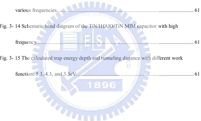
According to the latest International Technology Roadmap for Semiconductors (ITRS) [1-2], radio frequency and analog/mixed-signal technologies for wireless communication require capacitors with a capacitance density higher than 4fF/μm2 from year 2009 (Table 1- I). For oxide and silicon nitride in conventional MIM capacitors, their viability faces great challenges due to their low dielectric constants (k~3.9 for SiO2, ~7 for Si3N4). As we know, the
relationship between capacitance density and thickness is: d
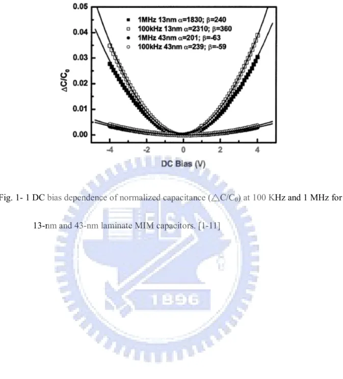
C , where C is the capacitance density, d present the dielectric thickness, and ε is the dielectric constant. Therefore, to increase capacitance density for higher circuit density, either thinner dielectric or higher dielectric constant material is better choice. However, leakage current and reliability issues limit the aggressive dielectric thickness scaling down. Therefore, high dielectric constant (high-k) materials seem to be an unavoidable choice. This requirement can be achieved even by using insulators with a dielectric constant higher than 57, and considering the present dielectric thickness of around 30 nm (the capacitance density is about to 16.8 fF/μm2). Material such as Ba, Sr, Ti, and Ta based oxide exhibit high dielectric constant values of 60 or above if crystallized by a high temperature annealing [1-3]-[1-4], which is however unrealistic in the backend of the line process. Instead, amorphous dielectrics such as Al2O3, Ta2O5, and HfO2 (Table 1- I)[1-5] have recently been investigated for MIM capacitor application [1-6]-[1-9]. Considering their high dielectric constant of 9 to 25, the dielectric thickness of these materials could be reduced to thinner than 20nm in order to meet the requirement for high-density bypass capacitor application. Use of thin dielectrics will however cause other problems such as leakage current.
However, there are still many challenges result from using high-k material as insulator. These challenges include voltage linearity Fig. 1- 1 [1-11]), capacitance density dependence of temperature, frequency dispersion, and leakage current.
The voltage linearity of metal-insulator-metal capacitors is expressed by voltage coefficient of capacitance (VCC) obtained from a second order polynomial equation of C(V)= C0(αV2+βV+1), where C0 isthe capacitance at zero bias and α and β represent the quadratic and linear VCC, respectively [1-10], as determined by using a second order polynomial curve fitting to the measured data. The mechanism of VCC dependence remains under study. Several explanations have been given, such as the presence of traps near the mental-insulator interface [1-15], the occurrence of free carrier space charge relaxation [1-16], or the nonlinearities of the metal-oxygen bond polarizability [1-17].
Moreover, the capacitance density of capacitor using high-k material shows a strong frequency dependence (Fig. 1- 1 [1-11]). These results are contrast to the MIM capacitors with SiO2 as dielectric. They show no frequency dependence and minimal VCC effects with bias. Low leakage current is also an essential requirement within the normal circuit bias conditions.
1.3 Motivation
dielectric constant (k=10~25) [1-13], low interface state density (comparing with pure HfO2) [1-12]. In this work, we use HfAlO as the insulator in MIM structure. We expect that the capacitance density and leakage current will meet the present requirement. Titanium nitride (TiN) is extensively to be used in MOSFET technology. Therefore, we use TiN as the top and bottom metal electrode in this work.
Furthermore, the capacitance degradation behavior of a single capacitor has not been well characterized. Besset et al. [1-14] depicted the MIM capacitance variation under electrical stress. There is a new model proposed by W. H. Wu [1-18]. On MIS structure (using high-k material), we found similar phenomenon: the capacitance increases with the decrease of frequency. On MIM structure (using high-k material), the capacitance increases at low frequency and higher bias. We supposed that the nonlinearity of the metal-insulator-metal also results from pre-existing trap near the interface between electrode and high-k layer. An improved model is proposed in this thesis.
1.4 The Organization of This Thesis
The organization of this thesis is briefly described below. Chapter 1 depicts the historical perspective to explain the VCC phenomenon and the motivation of this thesis. Chapter 2 describes the process flow of the MIM capacitors and the methods of electrical and material
the leakage current mechanism. Also, we compare the VCC behavior of the samples with different Al:Hf ratios and we use the improved model to find out the spatial and energy distribution of the pre-existed trap density which result in voltage nonlinearity. We also discuss the limitation of the improved model. Chapter 4 summarizes the conclusions and contributions of the thesis, and provides some suggestions for future works.
Table 1- I The requirement for RF device according to ITRS[1-2] Year of production 2008 2009 2010 2011 2012 2013 RF Metal-Insulator-Metal capacitor Density (fF/μm2) 4 4 5 5 5 7 Voltage linearity (ppm/V2) <100 <100 <100 <100 <100 <100
Leakage (A/cm2) <1e-8 <1e-8 <1e-8 <1e-8 <1e-8 <1e-8
Table 1- II Summarized material and electric properties of several high- κ gate dielectrics [1-5].
Fig. 1- 1 DC bias dependence of normalized capacitance (△C/C0) at 100 KHz and 1 MHz for 13-nm and 43-nm laminate MIM capacitors. [1-11]
Chapter2
Experimental Procedure
2.1 Device Fabrication
The starting material was 4-inches, (100)-oriented, and boron doped p-type silicon wafer with a resistivity of 0.0008 Ω-cm. Because the Si wafers were used to support the MIM structure, their quality is not important and control wafers were used. Wafers were cleaned by the standard RCA clean process to remove particles and metal ions, and followed by HF-dip to remove chemical oxide. Then the bottom electrode of 10nm thick TiN layer was deposited with TiCl4 as precursor at 350℃ by a plasma enhanced atomic layer deposition (PEALD) system. After bottom electrode deposition, HfAlO was also deposited by PEALD at 300℃. The reactants are HfCl4, Al(CH)3, and H2O. HfAlO films with two different Al percentages were deposited. For each kind of HfAlO film, there are three different thicknesses: 15nm, 25nm, 35nm. The thickness and Al percentage were controlled by the deposition cycle number. Sample ID and HfAlO conditions were listed in Table 2- 1. The top electrode was deposited in the same PEALD chamber as the bottom electrode. Finally, we deposited 20nm thick Pt film by sputtering method through a shadow mask with radius of 150m in circle. To divide the pattern, we use SC1 to etching back the top TiN film. Finally, we deposited Al in the backside
of wafers in order to increase the electric conductivity. The process flow and schematic cross-sectional drawings were shown in Fig.2-1.
2.2 Material and Electrical Analysis
The Hf:Al atomic ratio was analyzed by inductively-coupled-plasma mass-spectrometer (ICP-MS). The thickness of films and interfacial details were investigated by transmission electron microscope (TEM).
For electrical measurement, the leakage current-voltage characteristics were measured by a semiconductor parameter analyzer of model Agilent 4156C. The capacitance-voltage characteristics were measured by a precision impedance meter of model Agilent 4284A at frequencies varied from 1K to 1M Hz. The amplitude of the ac signal is 25mV.
2.3 Physical Models
As we know, the typical used parallel circuit model in Agilent 4284A is a resistance shunt with an ideal capacitor (shown in Fig.2-2(a) [2-1]). In our device, because of leakage current and unavoidable parasitic resistance, the simple parallel model resulted in an unreasonable capacitance due to the incorrect equivalent circuit under high frequency. Several equivalent circuit models have been proposed in these years [2-2]-[2-5]. In this work, we use
the five-element circuit model [2-1], which considers both the static and dynamic dielectric energy losses and parasitic components such as the substrate resistance and cable/system inductance. This five-element circuit model could be simplified as another two four-element circuit models to reduce the calculations, depending on the leakage current [2-1]. The proposed model is shown in Fig.2-2(b) [2-1]. In this five-element circuit model, Co is the ideal dielectric capacitance, Rp is the shunt resistance due to gate leakage current, tanδis the loss tangent due to dielectric energy absorption, Rs is the series resistance due to substrate and contact resistance, and Ls is the series inductance due to extension cables and the probing system. The formula used to correct the capacitance using two-frequency-method is:
(2- 1)
, where Co is the correct capacitance, is the measured frequency, G is the conductance, and Cp is the measured capacitance.
It has been reported that the capacitance of the HfO2 MIS structure decreases with the increase of measurement capacitance as shown in Fig.2-3. After correction, similar to the HfO2 MIS capacitor, the phenomenon of the decreasing capacitance with increasing frequency is observed in our MIM capacitors. In this work, we use HfAlO as dielectric layer. It is supposed that there must be something like border traps exist in the dielectric layer [2-6]-[2-7]. Following the physical model about border trap proposed by W. H. Wu, we made some
modification and adapt it to our MIM structure. We reduced the dielectric layers to a single layer, i.e., ignoring interfacial layer, the Nbt formula can be simplified as:
1 * 2 2 2 ( ) ( ) ln( ) c t bt m q x dC N x qA d f (cm -3 eV-1) (2- 2)
,where x is the tunneling distance from the bottom electrode, m* is the electron effective mass in HfAlO, Φc is the conduction band barrier height of HfAlO, q is the elementary charge, is the electric field, f is the measured frequency, is the Planck constant, and A is the area of electrode. Also, we can extract the trap energy depth and the tunneling distance by the formula as followed:
3 2 0 2 33
2
4
4
1
1
*/
)
ln(
)
/
(
/
qm
f
q
q
x
c c (2- 3) and t cE
q x
(2- 4), where x is the tunneling distance from the bottom electrode, m* is the electron effective mass in HfAlO, Φc is the conduction band barrier height of HfAlO, q is the elementary charge, is the electric field, f is the measured frequency, is the Planck constant, A is the area of electrode, and τ0 is the tunneling time constant pre-factor which is relative insensitive to the tunneling distance and trap energy depth, and it is assumed to be 10-10 sec for the charge exchange[2-1]. From the above formulas, the frequency and gate bias voltage dependences could be transformed into the relationships of the tunneling distance from the electron
injection electrode and the trap energy depth from HfAlO conduction band edge. Based on the physical model of elastic direct tunneling through trapezoidal potential barriers, the space and energy distribution of border traps of HfAlO capacitor could be profiled as a 3D-mesh.
Table 2- 1 Sample ID and HfAlO conditions. Sample Number Al:Hf atomic ratio Thickness (nm) 1 15 2 25 3 1:8.7 35 4 15 5 25 6 1:5.8 35
Fig.2-1 Process flow and schematic cross-sectional drawings of the TiN/HfAlO/TiN MIM capacitors.
Fig.2-2 (a) Typical parallel circuit model in Agilent 4284A (b) Five-element circuit model proposed by W. H. Wu [2-1].
Fig.2-3 Capacitance-voltage curves of the TiN/HfO2/SiO2/n-Si MOS capacitor measured and corrected at various frequencies [2-1].
Chapter3
Analysis of HfAlO MIM Capacitor
3.1 Introduction
HfAlO has attracted much attention because of its high thermal stability, wide band gap, and low leakage current [3-1]-[3-2]. However, it is also known that the MIM capacitors with high-k dielectric have strong voltage and frequency dependence on capacitance. These effects result in characteristic degradations of analog/mixed-signal circuits. At present, the cause of the voltage and frequency dependence in high-k MIM capacitors has not been clarified yet. In some reports, this behavior is related to the existence of interface traps which induce charges with different time constants and modulate the capacitance at certain frequencies [3-3]-[3-5]. However, the trap density and distribution have not been reported.
In this thesis, we proposed a modified model to extract the trap density, tunneling distance, and trap energy depth of the MIM capacitors with HfAlO dielectrics. Also, the basic electrical characteristics including leakage current mechanism and voltage coefficient of capacitance (VCC) will be investigated. The limitation of the modified model will be discussed in this chapter.
3.2 Material analysis
Fig. 3-2 shows the cross-sectional TEM micrographs of the TiN/HfAlO/TiN MIM capacitors. The thicknesses of dielectric layers are very close to what we estimated from the deposition rate and deposition cycles. The about 0.7nm thick interfacial layer at the TiN/Si interface is native SiO2 grown before TiN deposition due to the high doping concentration of the degenerate Si substrate. This layer may increase the series resistance of the MIM capacitors so that capacitance correction must be performed. The TiN thickness is not so accurate. What important is that no interfacial layer is observed at both the TiN/HfAlO and HfAlO/TiN interfaces. The inductively coupled plasma mass-spectrometer (ICP-MS) analysis identified that the Al/Hf atomic ratios of the two kinds of HfAlO films are equal to 1: 8.7 and 1:5.8.
3.3 Analysis of Capacitance Dependence on Voltage and
Frequency
The capacitances were measured from -3V to 3V at 1K, 10K, 100K, 500K, and 1M Hz. In order to eliminate the influences of parasitic components on the measured capacitance, all of the measured capacitances were corrected by the two-frequency C-V correction method using the five-element circuit model proposed by W. H. Wu [3-6]. Fig. 3- 3 compares the original and corrected capacitances. The parasitic parameters extracted at 3V and 1MHz from
the samples with 15nm-thick HfAlO and Al:Hf=1:8.7 are tan=0.0448, Rs=29, Rp= 2x10¹¹, and Ls=60H. These values are in the reasonable range. Table 3-I lists the capacitance density of all of the 6 samples calculated from the corrected capacitance measured at 3V and 1MHz. According to the 2007 ITRS, radio frequency and analog/mixed-signal technologies for wireless communication require capacitors with a capacitance density higher than 4fF/μm2 at year 2009. In our work, the capacitance density of all the 6 samples achieves the goal. The dielectric constant of the film with Al:Hf=1:8.7 is 23, and that of the film with Al:Hf=1:5.8 is 19.5. The higher Hf content is, the higher the dielectric constant is. Furthermore, the capacitance density is almost linearly dependent on the film thickness, which indicates that the interfacial layer is negligible.
The voltage coefficient of capacitance (VCC) is one of the important parameters for analog circuit application since high level of charge variation would result in the data loss and signal distortion [3-7]. Fig. 3- 4 shows the voltage linearity property of HfAlO MIM capacitors with applied voltage at various frequencies after capacitance correction. The capacitance of the MIM capacitor can be fitted by
2
0
(
1)
C
C
V
V
. (3- 1)Here, α is the quadratic VCC (ppm/V2), β is the linear VCC (ppm/V), C0 is the capacitance at
zero bias voltage, and V is the bias voltage. These two VCC parameters can be determined by using a second order polynomial curve fitting to the measured data.
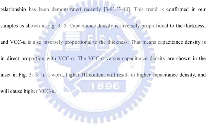
Fig. 3- 4 (a)-(f) depicts that the VCC-α is lower when the measured frequency is higher. In general, frequency dispersion is believed to be related to the existence of traps at electrode/dielectric interface. Different traps induce charges with different time constants and modulate capacitor charges strongly at certain frequency. Therefore, VCC-α is low at higher frequency because the induced charges are unable to follow the quick ac signal. In addition, VCC-α is known to be conversely proportional to the logarithmic dielectric thickness and this relationship has been demonstrated recently [3-8]-[3-10]. This trend is confirmed in our samples as shown in Fig. 3- 5. Capacitance density is inversely proportional to the thickness, and VCC-α is also inversely proportional to the thickness. That means capacitance density is in direct proportion with VCC-α. The VCC-α versus capacitance density are shown in the inset in Fig. 3- 5. In a word, higher Hf content will result in higher capacitance density, and will cause higher VCC-α.
3.4 Leakage current mechanism
The current densities of the TiN/HfAlO/TiN MIM capacitors are shown in Fig. 3- 6(a)-(b). The current density at 1V bias and 25℃of the Al:Hf=1:8.7 samples with dielectric thickness of 15nm, 25nm, and 35nm is 1.88×10⁻⁸, 6.67×10⁻⁹, and 2.37×10⁻⁹ (A/cm2), respectively. The current density of the Al:Hf=1:5.8 samples with dielectric thickness of 15nm, 25nm, and 35nm is 1.72×10⁻⁸, 1.88×10⁻⁹, and 7.9×10⁻¹⁰ (A/cm2), respectively. All of 6
samples meet the requirement of leakage current in 2007 ITRS [3-11].
To identify the leakage current mechanism of the TiN/HfAlO/TiN MIM capacitors with different ratios, Schottky emission (S-E) mechanism was examined at first. It is well known that the S-E mechanism, which the leakage current is electrode-limited and contributed by the carriers those overcome the barrier height between the electrode and the dielectric, has a linear ln(J/T2)-E1/2 relation as depicted by eq. (3- 2) and (3- 3)[3-12][3-13].
1 2 * 2
exp
E
bJ
A T
kT
(3-2) 1 3 2 0 4 q K (3-3), where A* denotes the Richardson constant, k is the Boltzmann’s constant, T is the absolute temperature(K), E is the applied external electric field, q is the electron charge, ε0 is the permittivity in vacuum, K∞ is the high-frequency dielectric constant [3-3] (=n2, where n is the refractive index), and ψb is corresponding to the barrier height between metal/dielectric. We have plotted ln(J/T2)-E1/2 curves for TiN/HflO/TiN MIM capacitors in Fig. 3- 7. The good linearity indicates that the leakage current is dominated by the S-E mechanism as the voltage is in the range of 0.3V-3V. The slope is the almost the same, and is independent on thickness. This indicates identical electrode/dielectric interface property. The Schottky barrier height (ψb) calculated from the intercept in Fig. 3- 7 is about 0.9-0.96eV. This value is lower than the
mechanism, we also examine the trap-assisted-tunneling (TAT) mechanism [3-14]. According to the TAT mode, the current-voltage characteristics can be expressed as :
3 2
4 2
~ exp(
/ )
3
ox t tqm
J
E
(3-4) Fig. 3-9 Fig. 3-1 shows the ln(Jt)-1/E plot. The calculated (10t-6
eV) indicates that the leakage current at medium field can not be fitted by the TAT model. It is thus suspected that the low Schottky barrier height (ψ0) is due to Fermi-level pinning, image force, surface states, and so on.
At very low field, the leakage current increases linearly with the increase of voltage bias as shown in Fig. 3-9. This linear relationship presents an ohmic conduction mechanism, which describe the thermal excitation of trapped electrons from one trap to another at low electric field [3-15].
To investigate the leakage current mechanism of the MIM capacitors at higher electric field, the ln(J/E) versus E1/2 plots with Al:Hf=1:8.7 and Al:Hf=1:5.8 are shown in Fig. 3-10. The Frenkel-Poole (F-P) conduction mechanism, which is a bulk-limited current and controlled by the detrapping of the electrons from the trap centers to the conduction band of the dielectric. The F-P effect can be described as by Eq. (3-5) and Eq. (3-6)[3-16, 3-17],
1 2 exp( E b) J BE kT (3-5) 1 3 2 0 ( q ) K (3-6)
, where B is the constant, T is the absolute temperature(K), E is the applied external electric field, q is the electron charge, ε0 is the permittivity in vacuum, K∞ is the high-frequency dielectric constant. Good linearity indicates that the leakage current is dominated by F-P tunneling at high electric field.
3.5 The trap density extracted from the improved physical model
Compared with the similar phenomenon that the capacitance dependence on frequency in MOS capacitors in W. H. Wu’s paper [3-6], we got the surmise that the pre-exist traps (named border traps) may also cause the capacitance dependence on frequency and applied voltage in MIM capacitors.The capacitance measured at low frequencies increase with the decrease of measurement frequency and the increase of applied voltage (as shown in Fig. 3- 4). The capacitance at low frequencies could be explained by proposing a frequency- and voltage-dependent border trap capacitance Cbt in parallel with the ideal dielectric capacitance C0 as shown in Fig. 3- 11 [3-6]. The border traps in high-k dielectrics could be detected by low-frequency capacitance-voltage (C-V) measurement, and this border trap capacitance is highly related to the measurement frequency and applied voltage.
formulas to extract the border trap density. 3 2 0 2 3 3 2 4 4 1 1
* / ) ln( ) / ( / qm f q q x c c (3-7) t cE
q x
(3-8) 1 * 22 2
(
)
( )
ln( )
c t btm
q x
dC
N
x
qA
d
f
(cm-3eV-1) (3-9), where x is the tunneling distance from the bottom electrode, m* is the electron effective mass in HfAlO, Φc is the conduction band barrier height of HfAlO, q is the elementary charge, is the electric field, f is the measured frequency, is the Planck constant, A is the area of the top electrode, and τ0 is the tunneling time constant pre-factor which is relative insensitive to the tunneling distance and trap energy depth, and it is assumed to be 10-10 sec for the charge exchange[3-6]. In our samples, m*=0.32m0 [3-18], the ideal Φc (the barrier height of HfAlO/TiN) is 2.2eV, which is obtained from the conduction band offset between Si and HfAlO (1.95 eV) [3-19], the Si electron affinity (4.05eV) and TiN work function (4.3eV) [3-20]. Fig. 3- 13 shows the space and energy distribution of border trap volume density Nbt (cm-3Ev-1) in the TiN/HfAlO/TiN MIM capacitor. The tunneling distance seems to be always larger than 0.7nm, and the detectable trap energy depth is very deep. These limitations will be discussed in the next section. The Nbt extracted at positive and negative bias from top electrode show almost the same energy and spatial distribution. It is reasonable because the MIM capacitor structure is symmetrical. The spatial distribution of Nbt saturates at a distance
of 1.2nm away from the electrode/dielectric interface. It is reasonable because traps density in bulk should be constant. However, the closer to the interface is, the lower Nbt is. This is not easy to understand. It may be a particular phenomenon in the narrow range of trap energy level.
Table 3- II lists the approximate Nbt of the 6 samples at the distance range of 1.2nm-1.5nm. We could figure out that the higher Nbt existed in the dielectric is , the more serious voltage nonlinearity (VCC-α) will be. Furthermore, the Nbt in W. H. Wu‘s paper [3-6] is about 1×10¹⁸~1×1020 cm-3eV-1, which is much higher than Nbt in this work (1×1017 cm-3Ev-1). We evaluate that the sample in [3-6] shows more serious voltage dependence and frequency dispersion (shown in Fig. 3- 14). The VCC- is about 1×10⁵ (ppm/V2) , which is 2 orders of magnitude higher than the VCC- of our TiN/HfAlO/TiN samples. This observation responds to our inference. The samples with higher Al content exhibit lower Nbt. This is consistent with the observation that Al can eliminate shallow traps in HfAlO film [3-21]. Because the dielectric thickness is not very thin and the detected Nbt is not very shallow, the Nbt should be independent of the dielectric thickness. However, the extracted Nbt slightly decreases as the dielectric thickness increases. This phenomenon might be attributed to the annealing effect during film deposition because thicker film experiences longer deposition time.
3.6 Limitation of the modified Physical model
In this section, we will discuss the limitations of the modified physical model. From the
tunneling distance formula:
3 2 0 2 3 3 2 4 4 1 1 * / ) ln( ) / ( / qm f q q x c c (3-7), we can
observe that the higher frequency will detect trap nearer the TiN/HfAlO interface. It is because the higher frequencies make the ac signal jump in and out quickly as shown in Fig. 3- 15. But in this thesis, we only measured the highest frequency up to 1M Hz due to the frequency limitation of Agilent 4284A precision LCR meter. We can observe that the tunneling distance is also dependent on the work function of the electrode. By mathematic method, when using higher work function-material as the electrode, the extracted tunneling distance will be nearer the TiN/HfAlO interface. To comprehend deeply, we modulate the work function and the measured frequency to detect the shallower tunneling distance. We fixed electric field and change the work function as 5.3, 4.3, and 3.3eV. The details were showed in Fig. 3- 16 . In conclusion, to detect the border trap nearer the interface, we have to measure at higher frequency or change higher work function-material as the electrode. Furthermore, to detect the shallower trap energy depth (Et), we can increase the applied electric field, which might cause breakdown. So, it is tradeoff between shallower energy depth and the breakdown happening.
Table 3-I The capacitance density with different Al/Hf ratio and thickness. Capacitance density (fF/μm2) 15nm 25nm 35nm Al:Hf=1:8.7 13.6 7.87 6.07 Al:Hf=1:5.8 11.3 7.7 5.03
Table 3- II The approximate Nbt and VCC-α of all samples.
Ratio Thickness Nbt (cm-3eV-1) Bottom Interface Nbt (cm-3eV-1) Top Interface VCC- α (ppm) at 1KHz Al:Hf=1:8.7 15nm ~2×10¹⁷ ~2×10¹⁷ 1549 25nm ~1×10¹⁷ ~1×10¹⁷ 556 35nm ~7×10¹⁶ ~7×10¹⁶ 360 Al:Hf=1:5.8 15nm ~1×10¹⁷ ~1×10¹⁷ 1519 25nm ~9×10¹⁶ ~9×10¹⁶ 541 35nm ~6×10¹⁶ ~6×10¹⁶ 309
(a)
(c)
(f)
Fig. 3-2 The TEM images of TiN/HfAlO/TiN MIM capacitors with(a) Al:Hf=1:8.7, 15nm-thick (b) Al:Hf=1:8.7, 25nm-thick(c) Al:Hf=1:8.7, 35nm-thick (d) Al:Hf=1:5.8, 15nm-thick (e) Al:Hf=1:5.8, 25nm-thick (f) Al:Hf=1:5.8, 35nm-thick.
Al:Hf=1:8.7_15nm
Frequency(Hz)
103 104 105 106C
a
p
a
c
it
a
n
c
e
(
F
)
0 3x10⁻¹⁰ 5x10⁻¹⁰ 8x10⁻¹⁰ 10-9 original data corrected data (a) Al:Hf=1:8.7 (25nm)Frequency(Hz)
103 104 105 106C
a
pa
c
it
a
n
c
e
(
F)
0 2x10⁻¹⁰ 4x10⁻¹⁰ 6x10⁻¹⁰ 8x10⁻¹⁰ original data corrected data (b)Al:Hf=1:8.7 (35nm)
Frequency (Hz)
103 104 105 106Cap
aci
tan
ce
(F
)
0 2x10⁻¹⁰ 4x10⁻¹⁰ 6x10⁻¹⁰ 8x10⁻¹⁰ 10-9 original data corrected data (c)Al:Hf=1:5.8_15nm
Frequency (Hz)
103 104 105 106C
a
pa
c
it
a
nc
e
(
F)
0 3x10⁻¹⁰ 6x10⁻¹⁰ 9x10⁻¹⁰ original data corrected data (d)Al:Hf=1:5.8 (25nm)
Frequency (Hz)
103 104 105 106C
a
p
a
c
it
a
n
c
e
(
F
)
0 2x10⁻¹⁰ 4x10⁻¹⁰ 6x10⁻¹⁰ 8x10⁻¹⁰ original data corrected data (e)Al:Hf=1:5.8 (35nm)
Frequency (Hz)
103 104 105 106C
a
p
a
c
it
a
n
c
e
(
F
)
0 10-10 2x10⁻¹⁰ 3x10⁻¹⁰ 4x10⁻¹⁰ original data corrected data (f)Fig. 3- 3 Comparison of the original and the corrected C_F characteristics with (a)-(f) Al:Hf=1:8.7 and Al:Hf=1:5.8 TiN/HfAlO/TiN MIM capacitors with dielectric thickness :15nm, 25nm, 35nm at 3V.
Al:Hf=1:8.7_15nm
Voltage (V)
-3 -2 -1 0 1 2 3(C
-C
o
)/
C
o
(
p
p
m
)
0 5000 10000 15000 20000 25000 1K_10K 100K_10K 500L_10K 1M_10K (a) Al:Hf=1:8.7 (25nm)Voltage(V)
-3 -2 -1 0 1 2 3(C-Co
)/
Co
(
p
p
m
)
0 5000 10000 15000 20000 1K_10K 100K_10K 500K_10K 1M_10K (b)Al:Hf=1:8.7 (35nm)
Voltage (V)
-3 -2 -1 0 1 2 3(C
-C
o
)/C
o
(
p
p
m
)
0 2000 4000 6000 8000 10000 12000 14000 1K_10K 100K_10K 500K_10K 1M_10K (c) Al:Hf=1:5.8_15nmVoltage (V)
-3 -2 -1 0 1 2 3(C
-C
o
)/
C
o
(
p
p
m
)
0 5000 10000 15000 20000 25000 1K_10K 100K_10K 500K_10K 1M_10K (d)Al:Hf=1:5.8 (25nm)
Voltage (V)
-3 -2 -1 0 1 2 3(C
-C
o
)/
C
o
(
p
p
m
)
0 2000 4000 6000 8000 10000 12000 1K_10K 100K_10K 500K_10K 1M_10K (e)Al:Hf=1:5.8 (35nm)
Voltage (V)
-3 -2 -1 0 1 2 3(C
-C
o
)/
C
o
(
p
p
m
)
0 2000 4000 6000 8000 10000 1K_10K 100K_10K 500K_10K 1M_10K (f)Fig. 3- 4 VCC-α versus voltage characteristics of Al:Hf=1:8.7 and Al:Hf=1:5.8 with dielectric thickness :15nm, 25nm, 35nm at 3V.
Al:Hf=1:8.7
Thickness (nm)
10 15 20 25 30 35 40
p
p
m
/V
2
100 1000 10000Capacitance density (fF/um2)
6 8 10 12 14 p p m /V 2 100 1000 10000 (a)
Thickness (nm)
10 15 20 25 30 35 40
p
p
m
/V
2
100 1000 10000 Al:Hf=1:5.8Capacitance density (fF/um2)
4 5 6 7 8 9 10 11 12 p p m /V 2 100 1000 10000 (b)
Fig. 3- 5 (a)Thickness dependence of VCC-α for the MIM capacitors with
Al:Hf=1:8.7. The inset shows VCC-α dependence on capacitance density (b)Thickness dependence of VCC-α for the MIM capacitors with
(b)
Fig. 3- 6 (a) Typical J-V characteristics of the MIM capacitors with Al:Hf=1:8.7 (b) Typical J-V characteristic of the MIM capacitors with Al:Hf=1:5.8.
(a)
(b)
Fig. 3- 7 (a) Schottky emission fitting of TiN/HfAlO/TiN capacitors with Al:Hf=1:8.7 (b) Schottky emission fitting of TiN/HfAlO/TiN capacitors with Al:Hf=1:5.8.
Al:Hf= 1:8.7_15nm |slope|: 22.4 & 3.92 at medium field
1/E (m/V)
0.0 0.1 0.2 0.3 0.4 0.5ln
(J
)
-20 -18 -16 -14 -12 -10Fig. 3-8 Trap-assist tunneling (TAT) model fitting of the TiN/HfAlO/TiN capacitors with Al:Hf=1:8.7. The slope at the linear region gives a value of 10t -6 eV. This unreasonable value indicates that the current transport is not dominated by the TAT mechanism.
(a)
(c)
(f)
Fig. 3-9 (a)-(f) Ohmic conduction fitting of 15nm, 25nm and 35nm-thick TiN/HfAlO/TiN capacitors with Al:Hf=1:8.7 and Al:Hf=1:5.8.
(a)
(c)
(e)
(f)
Fig. 3-10 (a)-(f) Fenkel-Poole conduction fitting of 15nm, 25nm and 35nm-thick TiN/HfAlO/TiN capacitors with Al:Hf=1:8.7 and Al:Hf=1:5.8.
Fig. 3- 11 The border trap capacitance in parallel with the ideal capacitance
Fig. 3- 12 Schematic band diagram of the TiN/HfAlO/TiN MIM capacitor biased at top electrode with illustration of tunneling distance and carrier energy coordinates.
(f)
Fig. 3- 13 (a)-(f) The space and energy distribution of border trap volume density Nbt (cm-3eV-1) of all samples at forward and reverse bias.
Fig. 3- 14 Capacitance-Voltage characteristics of the TiN/HfAlO/TiN MIM capacitors at various frequencies.
Fig. 3- 15 Schematic band diagram of the TiN/HfAlO/TiN MIM capacitor with high frequency.
Tunneling Distance (nm)
0.0
0.5
1.0
1.5
2.0
2.5
T
ra
p
E
n
e
rg
y
De
p
th
(
e
V
)
0
1
2
3
4
work function=5.3 eV work function=4.3 eV work function=3.3 eVFig. 3- 16 The calculated trap energy depth and tunneling distance with different work function: 5.3, 4.3, and 3.3eV
Chapter4
Conclusions
4.1 Summary
HfAlO has attracted much attention because of its high thermal stability, wide band gap, and low leakage current. The higher Hf content is, the higher capacitance density is. However, higher Hf content results in higher leakage current. It is a trade-off between capacitance density and leakage current density. In this thesis, we have two Al : Hf atomic ratios of 1:8.7 and 1:5.8. The dielectric constant is 23 for the HfAlO film with Al:Hf=1:8.7 and 19.5 for the HfAlO film with Al:Hf=1:5.8. The corresponded capacitance densities are 13.6 and 11.3 fF/ μm2
, respectively. The capacitance density achieves the ITRS requirement of a RF capacitor in 2013. The leakage current densities of 15nm-thick HfAlO film with Al:Hf=1:8.7 and Al:Hf=1:5.8 are 1.88×10⁻⁸ (A/cm2) and 1.72×10⁻⁸ (A/cm2) at 1V, respectively.
It is known that the MIM capacitors with high-k dielectric have strong dependence of capacitance on voltage and frequency. The effect of dielectric thickness, work-function of electrode, and film compositions on the parabolic voltage coefficient of capacitance (VCC-) was investigated in this thesis. The VCC-α in this thesis are 300(ppm/V2) (Al:Hf=1:8.7, 35nm-thick) and 259 (ppm/V2) (Al:Hf=1:5.8, 35nm-thick). Furthermore, a physical model
considering the pre-existing border traps was proposed to account for the VCC-. From the frequency and electrode bias voltage dependences the spatial and energy distribution from TiN surface and from HfAlOconduction band edge could be extracted, respectively. The orders of the magnitude of the extracted border trap volume densities are around 3×10¹⁷ (cm-3eV-1), which have positive correlation with the VCC-. Increasing the Al content can reduce the trap density and the VCC-. The limitations of detectable space and energy depth of the physical model are also discussed briefly. To detect the border trap nearer the interface, higher frequency or higher work function electrode are preferred. To detect shallower energy traps, higher work function electrode is preferred.
4.2 Future works
The high dielectric constant material in MIM capacitors was investigated for a long time. The most important challenge for RF capacitors is the voltage nonlinearity. The other mechanisms of the voltage nonlinearity may be existed. In this thesis, we also found that the VCC- has proportional relationship with the capacitance density. It is tradeoff between the VCC- and the capacitance density. Therefore, to find a high dielectric constant material with small VCC properties or combine negative VCC material such as SrTiO3 are both good research directions.
Reference
Chapter 1
[1-1] P. Zurcher, P. Alluri, P. Chu, A. Duvallet, C. Happ, R. Henderson, J. Mendonca, M. Kim, M Petras, M. Raymond, T. Remmel, D. Roberts, B. Steimle, J. Stipanuk, S. Straub, T. Sparks, M. Tarabbia, H. Thibieroz, and M. Miller“ Integration of Thin Film MIM Capacitors and Resistors into Copper Metallization based RF-CMOS and Bi-CMOS Technologies,” IEDM pp. 7.3.1-7.3.4, 2000
[1-2] International Technology Roadmap for Semiconductors (ITRS), 2007 edition.
[1-3] V. Dover, R. B. Fleming, R. M. Schneemeyer, L.F. Alers, and G.B Werder, “Advanced dielectrics for gate oxide, DRAM and RF capacitors” IEDM Tech. Dig., issue, 6-9, pp. 823–826, 1998
[1-4] G. B. Alers, V. Dover, R.B, Schneemeyer, L.F., L. Stirling, C. Y. Sung, P. W. Diodato, R. Liu, Y. H. Wong, R. M. Fleming, D. V. Lang, and J. P. Chang “ Advanced amorphous dielectrics for embedded capacitor,” in IEDM Tech. Dig, pp. 797–800., 1999
[1-5] H. S. P. Wong, “Beyond the conventional transistor,” IBM J. Res. Develop., vol. 46, no. 2/3, pp. 133-168, 2002
[1-7] H. Hu, C. Zhu, Y. F. Lu, M. F. Li, B. J. Cho, and W. K. Choi, “A high performance MIM capacitor using HfO dielectrics” IEEE Electron Device Lett., vol. 23, pp. 514–516, 2002
[1-8] T. Ishikawa, D. Kodama, and Y. Matsui, “High-capacitance Cu/Ta2O5/Cu MIM structure for SoC applicationsfeaturing a single-mask add-on process” IEDM Tech. Dig., pp. 940–944, 2002
[1-9] X. Yu, C. Zhu, H. Hu, A. Chin, M. F. Li, B. J. Cho, D.-L. Kwong, F. D.Foo, and M. B. Yu, “A high density MIM capacitor (13 fF/um ) using ALD/HfO dielectrics” IEEE Electron Device Lett., vol. 24, pp. 63–65, 2003
[1-10] K. S. Tan, S. Kiriake, M. de Wit, J. W. Fattaruso, C. Y. Tsay, W. E. Matthews, and R. K. Hester “Error correction techniques for high-performance differential A/D converters” IEEE J. Solid-State Circuits, vol.25, pp. 1318-1327, 1990
[1-11] H. Hu, S. J. Ding, H. F. Lim, Z. Chunxiang, M. F. Li, S. J. Kim, X. F. Yu, J. H. Chen, Y. F. Yong, J. C. Byung, D. S. H. Chan, S. C. Rustagi, M. B. Yu, C. H. Tung, D. Anyan, M. Doan, P. D. Foot, A. Chin, and L. K. Dim, “High-Performance MIM Capacitor Using ALD High-K HfO2–Al2O3 Laminate Dielectrics” IEEE Electron Device Lett., vol. 24, No. 12, pp. 15.6.1-15.6.4, 2003
[1-12] Y. K. Chioua, C. H. Changa, and C. C. Wanga, “Effect of Al incorporation in the thermal stability of atomic-layer-deposited HfO2 for gate dielectric applications” J.
Electron chem. Soc., Vol. 154, Issue 4, pp. G99-G102, 2007
[1-13] K. Takeda, R. Yamada, T. Imai, T. Fujiwara, T. Hashimoto, and T. Ando, “DC-stress-induced Degradation of Analog Characteristics in HfxAl(1-x)O MIM Capacitors” IEDM , 2006
[1-14] C. Besset, S. Bruyère, S. Blonkowski, S. Crémer and E. Vincent, “MIM capacitance variation under electrical stress” Microelectronics Reliability, vol. 43, pp. 1227-1240, 2003
[1-15] J. A. Babcock, S. G. Balstr, A. Pinto, C. Dirnecker, P. Steinmann, R. Jumpertz, and B. E. Kareh, “Analog Characteristics of Metal-Insulator-Metal Capacitors Using PECVD Nitride Dielectrics” IEEE electron Device Lett. vol, 22, pp. 230-232, 2001
[1-16] S. Blonkowski, M. Regache, and A. Halimaoui, “Investigate and modeling of the electrical properties of metal-oxide-metal structures formed from chemical vapor deposited Ta2O5 films” J. appl. Phys. vol. 90, pp.1501-1508, 2001
[1-17] S. Becu, S. Cremer, and J.-L Autran,” Microscopic model for dielectric constant in metal-insulator-metal capacitors with high-permittivity metallic oxides” Appl. Phys. Lett. vol. 88, pp.052902, 2006
Chapter 2
[2- 1] W. H. Wu, B. Y. Tsui, and M. C. Chen., “Electrical Characterization of Charge Trapping and De-trapping in Hf-Based High-k Gate Dielectrics” Electronics Engineering, National Chiao Tung University, 2006
[2- 2] K. J. Yang and C. Hu, “MOS capacitance measurements for high-leakage thin dielectrics” IEEE Trans. on Electron. vol. 46, pp. 1500-1501, 1999
[2- 3] A. Nara, N. Yasuda, H. Satake, and A. Toriumi, “Applicability limits of the two-frequency capacitance measurement technique for the thickness extraction of ultrathin gate oxide” IEEE Trans., vol. 15, pp.209-213, 2002
[2- 4] H. T. Lue, C. Y. Liu, and T. Y. Tseng, “An improved two-frequency method of capacitance measurement for SrTiO3 as high-k gate dielectric” IEEE Electron Device Lett., vol. 23, pp. 553-555, 2002
[2- 5] Z. Luo and T. P. Ma, “A new method to extract EOT of ultrathin gate dielectric with high leakage current” IEEE Electron Device Letters, vol.25, pp. 655-657, 2004
[2- 6] D. M. Fleetwood, “Border traps in MOS devices,” IEEE Trans. Nucl. Sci., 117 vol. 39, no. 2, pp. 269-271, Apr. 1992
[2- 7] D. M. Fleetwood, P. S. Winokur, R. A. Reber, T. L. Meisenhemer, J. R. Schwank, M. R. Shaneyfelt, and L. C. Riewe, “Effects of oxide traps, interface traps and border traps on metal-oxide-semiconductor devices,” J. Appl. Phys., vol. 73, pp. 5058-5074, 1993
Chapter 3
[3-1] W. J. Zhu, T. Tamagawa, M. Gibson, T. Furukawa, and T. P. Ma, “Effect of Al inclusion in HfO2 on the physical and electrical properties of the dielectrics,” IEEE Electron Device Letter, vol. 23, pp. 649–651, 2002
[3-2] K. Toriik, K. Shiraishi, S. Miyazaki, K. Yamabe, M. Boero, T. Chikyow, K. Yamadak, H. Kitajim, and T. Arikado, “Physical model of BTI, TDD Band SILC in HfO2-based high-k gate dielectrics,” IEDM Tech. Dig, pp. 129–132, 2004
[3- 3] L. I. Maissel and R. Glang, Handbook of thin film technology, McGraw-Hill, Ch. 14 pp. 25
[3-4] J. A. Babcock, S. G. Balster, A. Pinto, C. Dirmecker, P. Steinmann, R. Jumpertz, and B. E. Kareh, “Analog characteristics of metal-insulator-metal capacitors using PECVD nitride dielectrics,” IEEE Electron Device Lett., vol. 22, pp. 230-232, 2001
[3-5] H. Hu, C. Zhu, and Y. F. Lu, Y. H. Wu, T. Liew, M. F. Li, B. J. Cho, W. K. Choi and N. Yakovlev, “Physical and electrical characterization of HfO2 metal–insulator–metal capacitors for Si analog circuit applications” J. appl. Phys., vol. 94, pp. 552-557, 2003 [3-6 ] W. H. Wu, B. Y. Tsui, and M. C. Chen., “Electrical Characterization of Charge Trapping
and De- trapping in Hf-Based High-k Gate Dielectrics” Electronics Engineering, National Chiao Tung University, PHD., 2006
electronic devices,” J. Vac. Sci. Technol., vol. 18, pp. 1785-1791, May/Jun 2000
[3-8] X. Yu, C. Zhu, H. Hu, A. Chin, M. F. Li, B. J. Cho, D. L. Kwong, P. D. Foo, and M. B. Yu, "A high density MIM capacitor (13fF/um2) using ALD HfO2 dielectrics", IEEE Electron Device Lett. , vol. 24, pp. 63, 2003
[3-9] A. K. Roy, C. Hu, M. Racanelli, C. A. Compton, P. Kempf, G. Jolly, P. N. Sherman, J. Zheng , Z. Zhang, and A. Yin “High density metal insulator metal capacitors using PECVD nitride for mixed signal and RF circuits, ” IEEE Int. Interconnect Tech., Conf, pp. 245-247, 1999
[3-10] C. Zhu, H. Hu, X.Yu, S.J. Kim, A. Chin, M.F. Li, B. J. Cho, and D.L. Kwong, “Voltage and temperature dependence of capacitance of high-K HfO2 MIM capacitors: a unified understanding and prediction,” IEEE IEDM Tech. Dig. Int., pp. 879-882, 2003
[3-11] ”International Technology Roadmap for Semiconductors,” ITRS, 2007 edition.
[3-12] T. P. Juan, S. M. Chen, and J. Y. M. Lee, “Temperature dependence of the current conduction mechanisms in ferroelectric Pb(Zr0.53,Ti0.47)O3 thin film” J. Appl. Phys., vol. 95, issue 6, pp. 3120-3125, 2004
[3-13] C. Chaneliere, J. L. Autran and R. A. B. Devine, “Conduction mechanisms in Ta2O5/SiO2 and Ta2O5/i3N4 stacked structures on Si,” J. Appl. Phys, vol. 86, issue 1, pp. 480-486, 1999
oxides: A generalized trap-assisted tunneling model,” J. Appl. Phys., vol. 86, pp1488-1491, 1999
[3- 15] S. Ezhilvalavan and T. Y. Tseng, “Conduction mechanism in amorphous and crystalline Ta2O5 thin films,” J. Appl. Phys., vol. 83, pp.4797-4901, 1998
[3- 16] C. Lai, A. Chin, H. Kao, K. Chen, M. Hong, J. Kwo and C. Chi, “Very low voltage SiO2/HfON/HfAlO/TaN memory with fast speed and good retention,” IEEE VLSI Symp. Tech. Dig., pp. 54-55, 2006
[3- 17] C.H. Cheng, H.C. Pan, H.J. Yang, C.N. Hsiao, C.P. Chou, S.P. McAlister, and A. Chin, “Improved High-Temperature Leakage in High-Density MIM Capacitors by using a TiLaO Dielectric and in Ir electrode,” IEEE Electron Device Lett., vol. 28, pp. 1095-1097, 2007
[3- 18] V. Mikhelashvili, R. Brener, O. Kreinin, B. Meyler, J. Shneider, and G. Eisenstein, “Characteristics of metal-insulator-semiconductor capacitors based on high-k HfAlO dielectric films obtained by low-temperature electron-beam gun evaporation,” Appl. Phys. Lett., vol. 85, pp. 1346-1348, 2004
[3- 19] H. Y. Yu, M. F. Li, B. J. Cho, C. C. Yeo, M. S. Joo, D. L. Kwong, J. S. Pan, C. H. Ang, J. Z. Zheng, and S. Ramanathan, ” Energy gap and band alignment for (HfO2)x-( Al2O3)1-x on (100) Si,” Appl. Phys. Lett., vol. 81, pp. 376-378, 2002
and Al2O3-HfO2 MIM capacitors,” Microelectronics Reliability vol.43, pp. 1259-1266, 2003
[3-21] M. H. Lim, and B. Y. Tsui, “A study on the Properties of NiSi/High-K Film” Electronics Engineering, National Chiao Tung University, 2006
![Table 1- I The requirement for RF device according to ITRS[1-2] Year of production 2008 2009 2010 2011 2012 2013 RF Metal-Insulator-Metal capacitor Density (fF/μm 2 ) 4 4 5 5 5 7 Voltage linearity (ppm/V 2 ) <100 <100 <100 <](https://thumb-ap.123doks.com/thumbv2/9libinfo/8559970.188455/18.892.162.788.138.931/requirement-according-production-insulator-capacitor-density-voltage-linearity.webp)
![HPSH [ 氧化數平衡反應式係數 ]](data:image/gif;base64,R0lGODlhAQABAIAAAP///wAAACH5BAEAAAAALAAAAAABAAEAAAICRAEAOw==)