國 立 交 通 大 學
光電工程研究所
博 士 論 文
高介電係數介電質於五苯有機薄膜電晶體
及金氧半場效電晶體之研究
The Researches of High-κ Dielectrics
on Pentacene Based OTFTs and
MOSFETs
研 究 生:張明峯
指導教授:李柏璁 博士
荊鳳德 博士
高介電係數介電質於五苯有機薄膜電晶體
及金氧半場效電晶體之研究
The Researches of High-κ Dielectrics on Pentacene
Based OTFTs and MOSFETs
研 究 生:張明峯 Student: Ming-Feng Chang
指導教授:李柏璁 博士 Advisors: Dr. Po-Tsung Lee
荊鳳德 博士 Dr. Albert Chin
國立交通大學
光電工程研究所
博士論文
A Dissertation Submitted to Institute of Electro-Optical Engineering National Chiao Tung University in partial Fulfillment of the Requirements for the
高介電係數介電質於五苯有機薄膜電晶體
及金氧半場效電晶體之研究
研究生:張明峯
指導教授:李柏璁 博士
荊鳳德 博士
國立交通大學
光電工程研究所博士班
摘要
由於以五苯(pentacene)為主動層之有機薄膜電晶體可廣泛的應用於無線射頻 身分識別標籤、邏輯電路、顯示器驅動元件、感測元件,因此五苯有機薄膜電晶 體成為世界上各研發單位的重要研究課題之ㄧ,且在元件性能上屢有重大的突破 與進展。在本研究論文中,我們將探討高介電系數介電層在有機薄膜電晶體的應 用,並研究分析高介電系數介電層對於元件特性的改善。 首先我們製作與整合高介電系數氧化鉿鑭(HfLaO)介電層與氮化鉭(TaN)金 屬閘極於五苯有機薄膜電晶體,此元件量測到低的操作電壓、小的次臨界擺幅、 低的臨限電壓、良好的場效遷移率。此良好的元件特性可以說明氧化鉿鑭介電層上製作氧化鉿鑭/五苯有機薄膜電晶體。此元件也展現良好的元件特性,在低的 2.5 伏操作電壓下,量測到 0.13 V/decade 的次臨界擺幅、-1.24 伏的臨限電壓、0.13 cm2/V·s 的場效遷移率。 根據製作高介電系數氧化鉿鑭為介電層之五苯有機薄膜電晶體所得到的良 好電性,我們進一步發展使用高介電系數氮氧化鉿(HfON)為電荷捕捉層,在可撓 的聚亞醯胺基板上製作非揮發性五苯有機薄膜電晶體記憶體元件。利用高介電系 數介電材料氮氧化鉿為電荷捕捉層、氧化鉿鑭為電荷阻擋層和二氧化鉿(HfO2)為 電荷穿隧層,五苯有機薄膜電晶體記憶體元件可以得到低的寫入與抹除電壓。 最後我們探討在氮氧化矽(SiON)上,以高介電系數氧化鉿鋁(HfAlO)介電層 為覆蓋層去調變臨界電壓,使其適用於 p 型金氧半場效電晶體,我們也分析調變 臨界電壓的物理機制。在最佳1.5 奈米厚的氮氧化矽,氮化鉬(MoN)/氧化鉿鋁/氮 氧化矽p 型金氧半場效電晶體可得到 0.85 奈米的等效氧化層厚度、低的臨界電壓、 良好的次臨界擺幅、高的場效遷移率。平帶電壓朝正電壓方向改變被證明是由於 氧化鋁(Al2O3)與氮氧化矽的交互擴散與反應,形成氧化矽鋁(AlSiO)矽化物並造成 帶電的氧空缺。
The Researches of High-κ Dielectrics on Pentacene
Based OTFTs and MOSFETs
Student: Ming-Feng Chang Advisors: Dr. Po-Tsung Lee
Dr. Albert Chin
Department of Photonics & Institute of Electro-Optical Engineering
National Chiao Tung University
ABSTRACT
Due to the widespread applications such as radio frequency identification tags, logic circuits, display driver and sensors, the pentacene-based organic thin film transistors (OTFTs) are widely investigated and have many remarkable breakthroughs in performance. In this dissertation, we investigate the application of high dielectric constant (κ) dielectric to improve the performance and function of OTFTs.
First of all, we demonstrate the integration of HfLaO high-κ dielectric and TaN metal gate into pentacene OTFTs to get low operation voltage, small sub-threshold
process temperature to develop HfLaO/pentacene OTFT on flexible polyimide substrates. This device also shows good device integrity of a small SS of 0.13 V/decade
and a VT of −1.25 V and a good μ of 0.13 cm2/V·s at a low operating voltage of 2.5 V.
Based on the good electrical characteristics of pentacene OTFT incorporated with high-κ HfLaO dielectrics, we further use high-κ HfON as a charge trapping layer to develop organic pentacene non-volatile OTFT memory fabricated on flexible polyimide substrate. By using high-κ HfON as a charge trapping layer, HfLaO as a blocking layers
and HfO2 as a tunneling layer, the pentacene OTFT memory shows record low
program/erase voltage.
Finally, we study the High-κ HfAlO as a capping layer on SiON to modulate VT for
p-MOSFET application. The mechanisms of VT modulation also have been investigated.
Under the optimized 1.5 nm SiON, good device integrity of small 0.85 nm
equivalent-oxide-thickness, low Vt, good SS and high mobility are obtained in the
MoN/HfAlO/SiON p-MOSFETs. The large positive flatband voltage shift is explained due to the forming charged oxygen vacancies in AlSiO silicate, which is originated
Acknowledgements
能夠順利完成本論文,首先要感謝我的指導教授李柏璁教授和荊鳳德教授, 在兩位教授耐心的教導之下,學到了許多實驗的研究方法及待人處世應有的踏實 態度。 感謝鄧天王、阿甫、淳護、學人和迺超等學長的熱心指導,維邦、坤億、菘 宏和光揚等學弟的熱心幫忙,振昌、瑞晉和一德等同學的互相勉勵,還有各位學 弟熱情的給我意見,讓我可以更有信心完成我的實驗。也因為你們這群好學長好 同學讓我4年的博士班生涯過的很快樂與溫馨,希望大家以後都有美好的未來。 我也由衷感謝國科會與群創光電段總經理所提供的出國獎學金,讓我在博士 生涯中,有機會能夠在Yale大學馬教授實驗室從事短期研究,在美國期間除了一 圓我的留學夢之外,並增加我的國際觀和認識到許多好朋友。 最後感謝我親愛的老婆子婷陪我一路從碩士班到現在的博士班生涯,並支持 我所做的一切,讓我可以全心全力的朝自己的夢想邁進。Contents
Abstract (in Chinese)...i
Abstract (in English)...iii
Acknowledgements………...……….……….…....v
Contents...vi
Table Captions……….………..…………....………….ix
Figure Captions……….………..………....x
Chapter 1 Introduction
1.1. Overview of High-κ Gate Dielectrics………..…….………...………..11.2. Organic Thin Film Transistors……..………..………....…...3
1.2.1 Charge Transport in Organic Semiconductors………..………...4
1.2.2 The Operation Mode and Principles of OTFTs…...…………..……....……...6
1.2.3 Parameter Extraction of OTFTs……….…….….…….…...7
1.3. Motivation……….………...……….9
2.4. Summary……….21
Chapter 3 Small Sub-threshold-Swing and Low-Voltage, Flexible
Organic Thin Film Transistors which use HfLaO as the
Gate Dielectric
3.1. Introduction……….….………...293.2. Experimental Details……….………..30
3.3. Results and Discussion………....……....31
3.4. Summary……….………33
Chapter 4 A Flexible Organic Pentacene Nonvolatile Memory Base
on High-κ Dielectric Layers
4.1. Introduction………...….……….394.2. Experimental Details……….…………..………41
4.3. Results and Discussion………….……….………..41
4.4. Summary………..……….………..45
Chapter 5 Interfacial SiON Thickness Dependence on Device
Performance of High-κ MoN/HfAlO/SiON p-MOSFETs
5.1. Introduction……….……….………...55Chapter 6 Conclusions
……….………...70
References
……..……….………...72
Table Captions
Chapter 1 Introduction
Table 1-1. Comparison of relevant properties for high-k candidates [1.4]……….12 Chapter 2 Low Sub-threshold Swing HfLaO/Pentacene Organic Thin Film
Transistors
Table 2-1. Comparison of p-channel HfLaO/pentacene OTFTs with n-channel poly-Si TFTs……….……22 Chapter 3 Small Sub-threshold-Swing and Low-Voltage, Flexible Organic Thin
Film Transistors which use HfLaO as the Gate Dielectric
Figure Captions:
Chapter 1 Introduction
Fig. 1-1 Leakage current versus voltage for various thickness of SiO2 layers [1.1]...13
Fig. 1-2 Static dielectric constant versus band gap for candidate gate oxides [1.5]…14 Fig. 1-3 Molcular structure of common p-type organic semiconductors: Pentacene, 6T
(sexthiophene), P3HT (regioregular poly(3-hexylthiophene)), F8T2
(poly(9,9’dioctylfluorene-co-bithiophene)), PTAA (polytriarylamine), PVT (poly(2,5-thienylene vinylene)), DH-5T (α,ω-dihexylquinquethiophene), DH-6T (α,ω-dihexylsexithophene) [1.31]………..15 Fig. 1-4 Various device structures of OTFTs………...……16 Chapter 2 Low Sub-threshold Swing HfLaO/Pentacene Organic Thin Film
Transistors
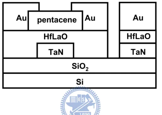
Fig. 2-1 Schematic diagram of HfLaO/pentacene OTFTs and Au/HfLaO/TaN MIM devices………...23
Fig. 2-4 ID-VD characteristics of HfLaO gate dielectric OTFTs with (a) and without (b)
NH3 plasma treatment………..…..26
Fig. 2-5 ID1/2-VG and ID-VG characteristics of HfLaO gate dielectric OTFTs with and
without NH3 plasma treatment………...………27
Fig. 2-6 AFM surface images of pentacene (5μm×5μm) on HfLaO/TaN with (a) and
without (b) NH3 plasma treatment………...…..28
Chapter 3 Small Sub-threshold-Swing and Low-Voltage, Flexible Organic Thin Film Transistors which use HfLaO as the Gate Dielectric
Fig. 3-1 A schematic diagram and image of the high-κ flexible HfLaO/pentacene OTFTs………..……..35 Fig. 3-2 (a) C–V and (b) J–V characteristics of Au/HfLaO/TaN capacitors…………36
Fig. 3-3 ID-VD curve for an HfLaO gate dielectric OTFT………...………37
Fig. 3-4 ID-VG and -ID1/2-VG of an HfLaO gate dielectric OTFT………..…….38
Chapter 4 A Flexible Organic Pentacene Nonvolatile Memory Base on High-κ Dielectric Layers
Fig. 4-1 (a) Schematic cross-sectional diagram and (b) Image of the flexible pentacene OTFT memory devices...47
Fig. 4-3 Band diagram of the TaN-HfLaO-HfON-HfO2-pentacene-Au OTFTs...49 Fig. 4-4 Capacitance-voltage hysteresis for the MIS structure, showing 3-4V
hysteresis. The curves are for different sets of program and erase voltages, as indicated...50
Fig. 4-5 (a) Drain current-Gate Voltage (ID-VG) hysteresis curves for a pentacene
OTFT memory device under VG = -12V, 1 ms program and VG = -12V, 100
ms erase conditions. The ID-VG curves were measured at VD = -1V. (b)
Capacitance-voltage hysteresis curves for a
TaN-HfLaO-HfON-HfO2-Pentacene-Au metal-insulator-semiconductor….51
Fig. 4-6 (a) Program characteristics and (b) erase characteristics of OTFT memory devices for different voltages and times. The erase characteristics were
initially programmed at Vg = -12V for 1ms. The Vth was extracted from the Id
-Vg curve at Vd = -1 V in the linear region……….…….52
Fig. 4-7 (a) Retention characteristics in terms of the threshold voltage, Vth, for the
High-κ MoN/HfAlO/SiON p-MOSFETs
Fig. 5-1. (a) C-V and (b) J-V characteristics of the MoN/HfAlO/SiON and control
MoN/SiON MOS capacitors before or after 1000oC RTA. The device area is
100μm×100μm………...63
Fig. 5-2. Vfb-EOT plot with different HfAlO thickness on constant 1.5 nm SiON…..64
Fig. 5-3. Si 2p XPS spectra of MoN/HfAlO/SiON/Si and control MoN/SiON/Si gate stacks with MoN layer etched back. Lowered peak energy was found after
1000oC RTA……….………..65
Fig. 5-4. C-V characteristics of MoN/HfAlO/SiON and control MoN/SiON MOS
capacitors with F+ implantation……….………66
Fig. 5-5. SIMS profiles of MoN/HfAlO/SiON gate stack (a) without and (b) with F+
implantation. The SiON thickness is 1.5 nm…………...………..67
Fig. 5-6. ID-VG characteristics of MoN/HfAlO/SiON p-MOSFETs……….…………68
Fig. 5-7. Hole mobility versus effective electric field of MoN/HfAlO/SiON and MoN/SiON p-MOSFETs………..……….69
Chapter 1
Introduction
1.1 Overview of High-κ Gate Dielectrics
As the physical thickness of Silicon dioxide (SiO2) based gate dielectric is small
than 1.5 nm, a number of fundamental problems arise in metal-oxide-semiconductor field-effect transistor (MOSFET). Below the physical thickness of 1.5 nm, the gate
leakage current exceeds the 1 A/cm2 due to tunneling mechanism as shown in Figure
1-1 [1.1]. To continue scaling down of SiO2 and to reduce gate leakage current,
hafnium-based high dielectric constant (high-κ) materials have been used to replace
SiO2 as gate dielectric at 45 nm node and beyond [1.2, 1.3].
From an electrical point of view, an MOSFET is a capacitance-operated device, where the source–drain current of the MOSFET depends on the gate capacitance.
t A
C=εoκ (1)
current.
Many high-κ materials have been studied as potential alternative gate dielectrics,
such as Ta2O5, TiO2, HfO2, ZrO2, Al2O3, La2O3, Si3N4 or mixtures of them or
metal-oxide-silicates of the mentioned compounds which have the κ values ranging from 7 to 80. For the aforementioned requirements, the κ value of high-κ material should be over 12, preferably 25-30. Unfortunately, each of these materials is found to have its drawbacks. There is a trade off with the band offset condition, which requires a reasonably large band gap to obtain acceptable gate leakage current [1.4, 1.5]. Table 1 and Figure 1-2 show that the κ value of candidate oxides tends to vary inversely
with the band gap. Al2O3 and Si3N4 were found to have small κ value <10, which can
not meet our future requirements. TiO2 has high-κ value of 80, but it is found to have
a low crystallization temperature of about 400 oC and low conduction band offset.
The κ value of all transition metal oxides is higher than SiO2. However, not
every high-κ oxide can be used as a gate dielectric material. The thermal SiO2, having
been used and studied intensively for more than 40 years, has excellent interface properties with the Si substrate. Instead, the high-κ materials are far less familiar to us and most of their properties are still unclear. For gate dielectric application, the high-κ
at required process temperatures. Moreover, they should have good interface properties with the channel materials so that the structure can have low interface trap density, high channel mobility, low oxide trap density, large band gap, and large band offset.
1.2 Organic Thin Film Transistors
Organic semiconductors have been studied since the late 1940s [1.6]. However, the first description of field effect in organic semiconductor was in 1970 [1.7, 1.8]. Figure 1-3 shows the molecular structures of several common p-type organic semiconductors. Organic thin film transistors (OTFTs) have been identified as potential elements of electronic devices since the report by Koezuka and coworkers using electrochemically polymerized polythiophene in 1986 [1.9]. The performance of OTFTs has undergone great progress, especially in the last several years. OTFTs have many advantages over conventional silicon technology: they can be fabricated at low cost, large area coverage and on flexible substrates. They have attracted considerable attention for use in a wide range of cost effective, high volume
of OTFTs based on rubrene single crystals was found to be 15.4 cm2 /Vs [1.17], which exceeds that of amorphous silicon (a-Si : H) devices.
1.2.1 Charge Transport in Organic Semiconductors
The primary difference between organic semiconductors and inorganic semiconductors is the nature of charge transport. In inorganic semiconductors, such as Si or Ge, the atoms are held together by strong covalent bonds. The strong covalent bonds between atoms lead to the existence of large conduction and valance band widths. The nature of charge transport in inorganic semiconductors is band-like as the system has definite order. The charge carrier mobility of inorganic semiconductors
such as single-crystalline Si is very high, of the order of 103 cm2/Vs. The carrier
mobility in inorganic semiconductors reduces with increasing temperature because the lattice vibrations (phonons) cause scattering.
However, the bonding between organic molecules is weak van der Waals forces. Band-like transport model is invalid in amorphous or organic semiconductors. The charge carrier mobility of organic semiconductors is several orders of magnitude lower than inorganic materials. The nature of charge transport in organic semiconductors is more of the hopping kind. Crystalline organic semiconductors can
materials and charge transfer takes place by hopping. Due to the charge carrier scattering at every step, the carrier mobility is significantly lower. In most organic semiconductors, the mobility increases with increasing temperature as hopping transport is assisted by phonons [1.18, 1.19].
The Multiple Trapping and Release (MTR) model is employed to explain charge transport in organic semiconductors [1.20]. The model suggests a narrow delocalized band be associated with a high concentration of localized levels that act as traps. At low gate voltages, a majority of charge carriers injected in the semiconductor get trapped in these localized states with the deep traps filling up first. As the gate voltage is increased, more traps get successively filled and the Fermi level approaches the valence band edge. In some cases, when a sufficiently high gate voltage is achieved, all trap states are filled and the subsequently injected carriers move with the mobility associated with carriers in the valence band [1.21, 1.22]. However, the temperature-independent mobility reported in some cases (Pentacene and oligothiophenes) is not accounted for by the MTR model [1.23-1.25]. Thus, the
molecular is exceeding to that limit, so that there is still controversy as to whether the conductivity in these materials should be described by localized or delocalized transport.
1.2.2 The Operation Mode and Principles of OTFTs
The general operation mode and structure of OTFTs are developed from insulated gate field-effect transistors fabricated from crystalline or amorphous inorganic semiconductors [1.30]. Figure 1-4 shows the common device configurations used in OTFTs. It is composed of three main components: source, drain, and gate electrodes; a gate dielectric; and an organic semiconductor as a channel layer. The p-type organic semiconductors such as pentacene or P3HT use Au, Pt, or Ni metals with high work function as source and drain electrode to form ohmic-like contact. Although the device structures of OTFTs and inorganic TFTs are similar, there are some differences in the operation mode.
The organic semiconductors are difficult to dope to another type. There are no P-N junctions in source and drain to reduce the off-state leakage current. The low off-state leakage current of OTFTs is due to low conductivity of organic semiconductors. The most OTFTs operate in accumulation or depletion modes that are
linear and saturation regimes as following:
At low drain voltage (VD), drain current (ID) increases linearly with VD (linear
regime) and is approximately determined from the following equation: ) 2 ( D T G i D V V V C L W I = μ − − , VD <VG −VT (2)
where L is the channel length, W is the channel width, Ci is the capacitance per unit
area, VT is the threshold voltage, VG is the gate voltage and μ is the field effect
mobility.
For higher VD, exceed VT, ID tends to saturate (saturation regime) due to the
pinch-off of the accumulation layer, and is modeled by the equation
2 ) ( 2 i G T D C V V L W I = μ − , VD >VG −VT (3)
1.2.3 Parameter Extraction of OTFTs
There are actually four important parameters to be determine the quality of OTFTs: mobility, threshold voltage, sub-threshold swing and on-off-state drive current ratio.
In the saturation regime, the mobility can be calculated by rewriting Equation (3) as: ) ( 2 i G T D C V V L W I = μ − (5)
Equation (5) predicts that plotting the square root of the saturation current
against VG would result a straight line. The mobility is obtained from the slope of the
line.
(2) Threshold voltage
Threshold voltage is defined as the onset voltage for the channel formation. The magnitude of threshold voltage corresponds to power consumption. It can be extracted
from Equation (5) by the x-intercept of ID1/2 −VG
plot. (3) sub-threshold swing
Sub-threshold swing (SS) controls the on-to-off voltage swing, and should be as
low as possible. The SS also represents the interface quality and is defined as
) 1 ( 10 ln log tan i it dep t cons V D G C C C q KT I V SS D + + × × = ∂ ∂ ≡ = (6)
where Cdep is the depletion capacitance density of semiconductor channel layer and Cit
is the capacitance density from charged interface traps. (4) on-off-state drive current ratio
(Ion/Ioff) can be helpful to define the logic level of digital signal. The Ion/Ioff represents
the ratio of the current when the device is turned on and when the device is in the off state. It is another important OTFTs characteristic and is given as
t qN V C I I A r G i off on μ μ 2 / = (7)
where μr and NA are the semiconductor mobility and carrier concentration (in the
off-state), respectively, t is the semiconductor film thickness, and q is the electron
charge. Therefore, the high Ion/Ioff can be obtained by large carrier mobility and a very
low off-conductivity value for the organic semiconductor. Note that Equations (7) are valid only when a number of conditions are satisfied [1.30, 1.31].
1.3 Motivation
Although the mobility of OTFTs is higher than 1 cm2/V.s, there are still several
electrical characteristics need to be improved such as threshold voltage, sub-threshold swing and operation voltage for commercial application. Therefore, how to enhance these characteristics is important.
On the other hand, the threshold voltage control is a critical issue of metal-gate high-κ MOSFETs. The flatband voltage is affected by the interface of High-κ
dielectric and SiO2. For this reason, we use high-κ HfAlO as a capping layer on SiON
to study the flatband voltage shift and device performance of MoN/HfAlO/SiON
p-MOSFETs.
1.4 Dissertation Organization
This dissertation is organized as follow:
In Chapter 2, we discuss the device performance of OTFTs that incorporates high-κ HfLaO as the gate dielectric. The effects of surface treatment on TaN gate electrode are discussed along with the electric characteristics of OTFTs. The focus of this research is the integration of pentance based OTFT with high-κ HfLaO to reach
good electrical characteristics such as a low SS and small VT.
In Chapter 3, we study the integration of pentacene OTFTs with a high-κ HfLaO dielectric onto flexible substrates.
In order to further extend the function of OTFTs, we develop a pentacene OTFT nonvolatile memory fabricated on a flexible polyimide substrate in Chapter 4. This memory function has been achieved by using a high-κ dielectric as charge trapping,
HfAlO capping SiON p-MOSFETs is mentioned in Chapter 5. The mechanisms of flatband voltage shift are discussed. By optimizing thickness of SiON, the good device performance of MoN/HAlO/SiON p-MOSFET can be reached.
Table 1-1 Comparison of relevant properties for high-k candidates [1.4]. Material Dielectric constant (κ) Band gap (ev) ΔEc (ev) to Si Crystal Structure SiO2 3.9 9 3.2 Amorphous Si3N4 7 5.3 2.4 Amorphous Al2O3 9 8.8 2.8 Amorphous Y2O3 15 6 2.3 Cubic La2O3 30 6 2.3 Hexagonal, cubic Ta2O5 22 4.4 0.35 Orthorhombic
TiO2 80 3.5 0 Tetragonal (rutile, anatase)
HfO2 25 5.8 1.4 Monoclinic, Tetragonal, Cubic
Fig. 1-3. Molcular structure of common p-type organic semiconductors: Pentacene, 6T (sexthiophene), P3HT (regioregular poly(3-hexylthiophene)), F8T2
Chapter 2
Low Sub-threshold Swing HfLaO/Pentacene
Organic Thin Film Transistors
2.1 Introduction
Poly-Si thin-film transistors (TFTs) [2.1]-[2.6] are currently used for active matrix liquid crystal displays (AMLCDs) on glass substrates. These poly-Si TFTs are
operated in inversion mode, and the ion-implantation for the n+ source-drain requires
activation using furnace annealing at 600oC, typically for ~12 hours. This extended
annealing slows down the process sequence and the large thermal budget is unfavorable for environment energy conservation. In contrast, organic TFTs (OTFTs) [2.7]-[2.9] can be processed with a significantly lower thermal budget, and without requiring ion implantation or an extended dopant activation period. This is because the OTFTs can be operated in the accumulation mode, where ohmic-like source-drain
issues. Besides displaying a high-κ value of up to 24, HfLaO permits low-temperature processing due to the strong metal-oxide bond enthalpy of both Hf-O
and La-O [2.13]. The adding La2O3 into HfO2 is especially important to decrease the
leakage current at low temperature process due to the larger conduction band offset of
La2O3 (2.3 eV to Si) than that of HfO2 (1.5 eV to Si) [2.14]. The HfLaO MOSFET
also shows less Fermi-level pinning than using HfO2 [2.10]-[2.12].
2.2 Experimental Details
The devices were fabricated on a thick SiO2 layer grown on Si wafers to mimic
poly-Si TFTs fabricated on glass substrates [2.2]. A 50 nm thick TaN gate electrode
was then deposited on the SiO2/Si, through a shadow mask, using reactive sputtering.
The surface of the TaN gate was subsequently treated with an NH3 plasma to improve
the gate leakage current [2.14]-[2.16]. Such nitrogen plasma treatment is the key
factor to achieve low leakage current and small EOT in previous DRAM capacitors [2.14]-[2.16]. The 20 nm thick HfLaO gate dielectric was then deposited by electron
beam evaporation and annealed in O2 at 350oC for 10 min. Next, pentacene (Aldrich
Chemical Co.) was evaporated through a shadow mask onto the sample to form an active layer 70 nm thick. This evaporation was performed at a deposition rate of 0.5
μm and width of 2000 μm. We also deposited Au directly onto HfLaO/TaN to make
200×200 μm2 capacitors to analyze the dielectric properties. The devices were
characterized using an HP4156C semiconductor parameter analyzer and an HP4284A precision LCR meter, under dark and air ambient conditions.
2.3 Results and Discussion
In Figure 2-1 we show the schematic diagram of OTFT. The J-V characteristics
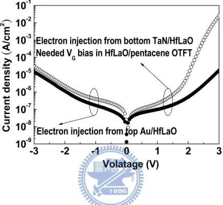
of Au/HfLaO/TaN capacitors are shown in Figure 2-2. The NH3 plasma treatment
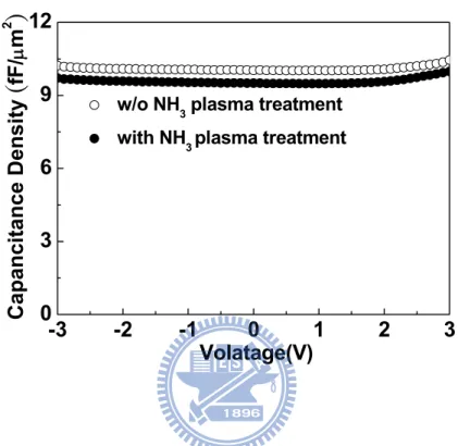
improves the leakage current of both electron injection from top Au/HfLaO and bottom HfLaO/TaN with close capacitance density shown in Figure 2-3. It is important to notice that the leakage current is much worse as electron injected from bottom interface, which is consistent with previous Analog/RF and DRAM MIM capacitors [2.14]-[2.16]. However, such bottom electron injection is needed for the
negative VG used in p-channel OTFTs. The data with NH3 plasma treatment indicate a
leakage current of 5.1×10⁻⁷ A/cm2 at 2 V, at a capacitance density as high as 950
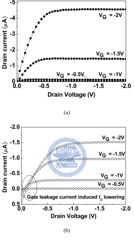
The output characteristics (ID-VD) of a high-κ HfLaO/pentacene OTFT are
displayed in Figure 2-4. The ID-VD characteristics with NH3 plasma treatment are
well-behaved, and suggest possible operation at 2 V, which has the advantage of
reducing the power consumption (ID×VD) in circuit operations. The ID-VD curves
without NH3 plasma treatment show poor characteristics that are due to high gate
leakage current induced ID lowering. The transfer characteristics (ID-VG), as shown in
Figure 2-5, enable the extraction of the mobility (μ) and threshold voltage (VT) from
the –ID1/2 vs. VG plot. The device with NH3treatment improves on current (Ion), SS and
off current (Ioff). The Ion improvement is not due to the pentacene, since the surface
roughness and grain sizes are similar shown in Figure 2-6. The performance
improvements are due to NH3 plasma treatment to reduce gate leakage current. The
device with NH3 plasma treatment shows a record small SS of only 78 mV/decade, a
VT of -1.3 V, and a good μ of 0.71 cm2/V.s, along with an on-off-state drive current
ratio (Ion/Ioff) as high as 1.0×10⁵. To analyze the low SS, we used the relationship:
) 1 ( 10 ln i it dep C C C q KT SS = × × + + (1)
where Cdep is the depletion capacitance density of pentacene, Cit is the capacitance
that for poly-Si TFTs [2.1]-[2.6] and OTFTs [2.7]-[2.9] and is close to theoretical minimum value of 0.06 V/decade at room temperature. We attribute these results to
the high Ci of 950 nF/cm2 and small EOT of 3.6 nm, resulting from the use of
advanced high-κ HfLaO dielectric even processed at low temperature.
The important device parameters are detailed in Table I, where the data from conventional n-channel poly-Si TFTs using solid phase crystallization (SPC) and
LPCVD or PECVD oxides [2.3]-[2.5] are included for comparison. Note that the μCi
term is directly related to ID (W/2L×μCi(VG-VT)2), normalized to the channel length L,
channel width W, and over-drive voltage of VG-VT. The performance of our HfLaO
OTFTs is comparable with that of poly-Si TFTs, which incorporate LPCVD and PECVD TEOS oxides [2.3]-[2.5], but with the additional merits of a better SS, lower
VT, faster process sequence and lower thermal budget process.
2.4 Summary
We have fabricated and characterized low voltage OTFTs that incorporate high-κ HfLaO as the gate dielectric. These devices exhibit good electrical
Table 2-1 Comparison of p-channel HfLaO/pentacene OTFTs with n-channel poly-Si TFTs. HfLaO LPCVD SiO2 PECVD TEOS oxide PECVD TEOS oxide Gate dielectric 20 nm 80 nm [2.3] 60 nm [2.4] 40 nm [2.5] Conduction channel thermally evaporated
pentacene poly-Si by SPC poly-Si by SPC poly-Si by SPC
Ci(nF/cm2) 950 43.1 57.5 86.3 VT (V) -1.3 5.6 8.14 Not extracted μ (cm2/Vs) 0.71 20 12.44 3 SS (V/decade) 0.078 1.4 1.97 2.67 μCi (nF/Vs) 674.5 862.8 715.7 258.8
Fig. 2-1. Schematic diagram of HfLaO/pentacene OTFTs and Au/HfLaO/TaN MIM devices.
-3 -2 -1 0 1 2 3 10-9 10-8 10-7 10-6 10-5 10-4 10-3 10-2 10-1
Electron injection from bottom TaN/HfLaO
Needed VG bias in HfLaO/pentacene OTFT
C u rr ent density
(
A/c m 2)
Volatage (V) Electron injection from top Au/HfLaOFig. 2-2. Leakage current comparison of Au/HfLaO/TaN capacitors with and without
-3 -2 -1 0 1 2 3 0 3 6 9 12 Capancitance Density
(
fF/ μ m 2)
Volatage(V)w/o NH3 plasma treatment
with NH3plasma treatment
Fig. 2-3. C-V characteristics of Au/HfLaO/TaN capacitors with and without NH3
0.0 -0.5 -1.0 -1.5 -2.0 0 -1 -2 -3 -4 -5 VG = -0.5V VG = -1V VG = -1.5V VG = -2V D rain cur re nt
(
μ A)
Drain Voltage (V) (a) 0.0 -0.5 -1.0 -1.5 -2.0 0.5 0.0 -0.5 -1.0 -1.5 -2.0 VG = -0.5V VG = -1V VG = -1.5V VG = -2V D rain current(
μ A)
Drain Voltage (V)Gate leakage current induced ID lowering
(b)
Fig. 2-4. ID-VD characteristics of HfLaO gate dielectric OTFTs with (a) and without (b)
-2.0 -1.5 -1.0 -0.5 0.0 0.0 4.0x10⁻⁴ 8.0x10⁻⁴ 1.2x10⁻³ 1.6x10⁻³ 2.0x10⁻³ 10-11 10-10 10-9 10-8 10-7 10-6 10-5
with NH3 plasma treatment
w/o NH3 plasma treatment
[
ABS(
Dr ain Cur re nt)]
1/ 2 (A ) 1/ 2 Gate voltage (V) VD= -2V ABS (Dr ain cur rent) (A)Fig. 2-5. ID1/2-VG and ID-VG characteristics of HfLaO gate dielectric OTFTs with and
(a)
Chapter 3
Small Sub-threshold-Swing and Low-Voltage,
Flexible Organic Thin Film Transistors which
use HfLaO as the Gate Dielectric
3.1 Introduction
Pentacene-based organic thin-film transistors (OTFTS) have been intensely
investigated due to their low cost and light weight, for potential use in applications such as flexible displays and low-cost flexible integrated circuits (IC) [3.1]-[3.3]. The low thermal budget and rapid processing have strong merits of energy saving and
environment friendly, which in sharp contrast to the extended 600oC annealing times
in conventional solid-phase crystallized (SPC) poly-Si TFTs. Although low thermal budget poly-Si TFTs can also be formed on plastic substrate using excimer laser annealing [3.4]-[3.5], the uniformity is a concern. Alternatively, poly-Si TFTs [3.6] or even single crystal sub-μm MOSFETs [3.7] can be realized on plastic substrate by
gate dielectrics have been applied in OTFTs for low–voltage operation [3.1], [3.3],
[3.11]-[3.14]. In chapter 2 we have studied pentacene OTFTs, on SiO2/Si substrates
using high-κ HfLaO as the gate dielectric. Although the performance is comparable
with SPC poly-Si TFTs, the process temperature of 350oC is still not suitable for
flexible electronics. In this work we further decrease the process temperature to 200oC
and demonstrate HfLaO/pentacene OTFTs, fabricated on low-cost flexible polyimide (PI) (Kapton HPP-ST, Dupont) substrates. These substrates are much more economical than other PI (Kapton E-type, Dupont) substrates [3.1], [3.11] and those which use polyethylene naphthalate (Teonex Q65 PEN, Dupont) [3.2].
3.2 Experimental Details
All the devices were fabricated on 125 μm thick PI substrates (Kapton HPP-ST, Dupont). Prior to the device fabrication process, the PI substrates were annealed in
vacuum environment (3×10⁻⁶ torr) at 200oC [3.2]. A 100 nm SiO
2 thin film was
deposited on the PI substrate by electron beam evaporation to ensure a low internal stress [3.3]. Then a 50 nm TaN gate electrode was deposited by reactive sputtering,
through a shadow mask. The surface of the TaN gate was treated in an NH3 plasma to
Chemical Co.), 70 nm in thickness, was deposited through the shadow mask. A
deposition rate of 0.5 Å/s, at a pressure of 3×10⁻⁶ torr was used, with a temperature of
the substrate at 70oC. Finally, 50 nm of Au was deposited for the source/drain
electrodes. The channel width and channel length were 2000 and 100 μm, respectively.
Metal-insulator-metal (MIM) Au/HfLaO/TaN capacitors, 200×200 μm2 in size, were
also fabricated to analyze the leakage current and the dielectric properties. All electrical characteristics were measured using an HP4156C semiconductor parameter analyzer and an HP4284A precision LCR meter in the dark and an air ambient.
3.3 Results and Discussion
We show a schematic diagram and image of the OTFTs in Figs. 1(a) and (b). The
C-V and J-V characteristics of the Au/HfLaO/TaN capacitors are detailed in Fig. 2 (a)
and (b) respectively. A low leakage current of 3.5×10⁻⁶ A/cm2 at 2.5 V was measured,
along with a capacitance density of 450 nF/cm2. This density yields an
equivalent-oxide-thickness (EOT) of 7.7 nm and a high-κ value of 15.3.
on-off-state drive current ratio (Ion/Ioff) was 1.2×10⁴. These values make the device
suitable for high-switching-speed, low-power ICs. The SS controls the on/off voltage swing, and should be small. The SS of our device is better than values observed for other flexible pentacene OTFTs [3.1]-[3.3], [3.11], [3.12]. The low SS value arises from the high gate capacitance density and small EOT. The relatively smaller mobility
and Ion/Ioff were due to both lower operation voltage and poor surface roughness. A
rms surface roughness of 4.3 nm was measured by Atomic Force Microscopy (AFM) on HfLaO and worse than the 2.0 nm value of BZN [3.3], which is originated from the poor 9.0 nm roughness of very low cost PI substrate (Kapton HPP-ST, Dupont).
In Table 3-1 we summarize some important device parameters, including other
data of low-voltage flexible pentacene OTFTs using Bi1.5Zn1.0Nb1.5O7 (BZN),
polyvinylphenol (PVP), Ta2O5, TiSiO2 and Mn-doped Ba0.6Sr0.4TiO3 (Mn-doped BST)
as gate dielectrics, and fabricated on high quality PI (Kapton E-type) and PEN substrates [3.1]-[3.3], [3.11], [3.12]. The low-voltage OTFTs using
(2-anthryl)undecoxycarbonyldecylphosphonic acid (π-σ-PA1)/AlOx,
octadecylphosphonic acid (OPDA)/AlOx and HfLaO as gate dielectrics, fabricated on
The performance of our HfLaO OTFTs is comparable with other low-voltage flexible pentacene OTFTs for low-power applications, but with the additional merit of a good
SS and the use of economical PI substrates.
3.4 Summary
A high-κ HfLaO dielectric was successfully integrated into pentacene OTFTs fabricated on low-cost flexible substrates. The electric characteristics of these HfLaO/pentacene OTFTs showed a low SS of only 0.13 V/decade, a high
gate-capacitance-density of 450 nF/cm2, a low VT of -1.25 V, a good μ of 0.13 cm2/Vs
and a Ion/Ioff of 1.2×10⁴. This superior performance permits the devices to be operated
at 2.5 V, which could be useful in flexible electronics.
Table 3-1 Comparison of low voltage OTFTs with various gate dielectrics. OTFTs with various gate dielectrics HfLaO [This work] BZN [1] PVP [2] Ta2O5 [3] Mn-doped BST [11] TiSiO2 [12] π-σ-PA1 /AlOx [13] OPDA/ AlOx [14] HfLaO substrate PI Kapton HPP-ST PI Kapton E-type PEN PEN PI Kapton E-type
PEN Si glass SiO2/Si
Dielectric thickness (nm) 30 200 50 150 200 136.4 - - 20 Operating voltage (V) 2.5 2 8 12 10 5 3 2 2 Ci (nF/cm2) 450 221 63.7 141.6 110 142.1 760 600~800 950 VT (V) -1.25 0.1 - 0.8 -1 -0.88 -1.3 0.35 -1.3 μ (cm2/Vs) 0.13 0.5 0.1 0.25 0.32 0.67 0.18 0.04 0.71 SS (V/decade) 0.13 0.3 0.6 - - 0.315 0.085 0.11 0.078 μCi (nF/Vs) 58.5 110.5 6.37 35.4 35.2 95.21 136.8 24~32 674.5 Ion/Ioff 1.2×10⁴ 3.5×10⁵ 1×10⁴ - <1×10³ 1×10⁴ 1×10⁵ 1×10⁴ 1×10⁵
(a)
SiO
2TaN
Au
Au
PI
HfLaO
pentacene
-2 -1 0 1 2 4.4 4.5 4.6 Capacitance density ( fF/ μ m 2 ) Voltage (V) (a) -3 -2 -1 0 1 2 3 10-9 10-8 10-7 10-6 10-5 10-4 Current density ( A/c m 2
)
Voltage (V) (b)0.0 -0.5 -1.0 -1.5 -2.0 0.0 -0.2 -0.4 -0.6 -0.8 -1.0 VG = - 1.2V VG = - 1.6V VG = - 2.0V VG = - 2.4V Drain current ( μ A ) Drain Voltage (V)
-2.5 -2.0 -1.5 -1.0 -0.5 0.0 0.0000 0.0005 0.0010 0.0015 10-13 10-12 10-11 10-10 10-9 10-8 10-7 10-6
[
ABS(
Drain C u rrent)]
1/2 (A) 1/ 2 Gate Voltage (V) IG VD= - 0.5V VD= - 2V AB S (Drain C u rrent ) (A )Chapter 4
A Flexible Organic Pentacene Nonvolatile
Memory Base on High-κ Dielectric Layers
4.1 Introduction
Organic non-volatile memory devices have potential applications in flexible display drive logic, radio frequency identification tags and smart cards [4.1, 4.2]. These non-volatile memory devices supply an essential function for integrated circuits (ICs) based on organic thin-film transistors (OTFTs). The advantages of using organic memory devices, over their inorganic counterparts, are in their low cost, light weight, simple structure, mechanical flexibility, and low-temperature processing. The OTFT-based non-volatile organic memory devices display high drive current, low off-state leakage current and reasonably-fast switching speeds. The memory properties of these OTFT-based devices arise from the electric field modulation in the
removing the stored charges. This charge transfer in the gate dielectric is readable by
measuring the threshold voltage (VT) of the transistor. This program or erase function
can be obtained by having a large electric field across the gate insulator. Previous
charge-trapping OTFTs have used a polymer as the insulator[4.5] or a floating gate
[4.6] – necessitating a high gate voltage (VG) to write the data. Such high voltages are
incompatible with low-power IC designs and challenge existing battery technology. A solution to lowering the program and erase voltages is to use a high-κ dielectric. This has been done by incorporating a high-κ dielectric as the gate insulator in the OTFTs, leading to lower voltage operation [4.7-4.9].
Here we demonstrate a pentacene OTFT non-volatile memory, fabricated on a flexible polyimide (PI) substrate, which shows a program/erase voltage of 12 V, speed of 1 ms/100 ms, initial memory window of 2.4 V and a 0.78 V memory window after 48 hours. This has been achieved by using a high-κ dielectric as charge trapping-, blocking- and tunneling gate insulator layers. This yields to similar program/erase voltages as in charge trapping non-volatile memory devices in Si technology
[4.10-4.14]. The magnitude of the VT writing voltage can be decreased to 6 V by
4.2 Experimental Details
The OTFT memory devices were fabricated on 125 μm thick PI substrates (Kapton HPP-ST, Dupont). Prior to device fabrication, the substrates were cleaned in
de-ionized water and annealed in a vacuum (3×10⁻⁶ torr) at 200°C - to improve the
dimension stability. A 100 nm SiO2 thin film was deposited on the substrate by
electron beam evaporation to create a layer with low internal stress. A 50 nm TaN gate electrode was then deposited by reactive sputtering, through a shadow mask. This
was given a NH3 plasma treatment to improve the metal-electrode/high-κ interface
[4.9]. The 20 nm HfLaO, 20 nm HfON and 6 nm HfO2 were then deposited by
physical vapor deposition and given a 200°C, 30 minute furnace treatment in O2, to
improve the gate oxide quality. This was followed by deposition, through a shadow mask, of the pentacene active layer (Aldrich Chemical Co.), 70 nm in thickness. (The
deposition conditions were: - a deposition rate of 0.5 Å/s, at a pressure of 3×10⁻⁶ torr,
with the substrate being held at 70°C.) Finally, 50 nm of gold was deposited, at rate of 1 Å/s, for the source/drain electrodes. The channel width and channel length were
A schematic diagram of the OTFT non-volatile memory is shown in Figure 4-1(a) and a corresponding image in Figure 4-1(b). The structure comprises a TaN gate
electrode, HfLaO charge blocking dielectric, HfON charge trapping layer, HfO2
charge tunneling dielectric, pentacene semiconductor layer and gold electrodes for the source-drain contacts. Output and transfer characteristics for such a device are displayed in Figures 4-2(a) and 4-2(b). From the transfer characteristics, the mobility,
VT, sub-threshold swing (SS) and on/off current ratio (Ion/Ioff) were 0.1 cm2V-1s-1, -1.4
V, 160 mVdec-1 and 1×10⁴ in the saturation region at a drain voltage (VD) of -3 V. The
low VT and good SS are due to the use of a high-κ material as gate the dielectric
[4.7-4.9].
The energy band diagram our OTFT memory device [4.15, 4.16] is shown in Figure 4-3. The HfLaO gate dielectric has a high dielectric constant, large bandgap and high electron injection barrier with respect to the TaN gate electrode during the erase process [4.9]. The small band-gap HfON, [4.10-4.12] with its deep trapping energy, was chosen as the charge-trapping layer to achieve good charge trapping
characteristics. The thin HfO2 dielectric serves as a charge-tunneling layer. The gold
A Metal-Insulator-Semiconductor (MIS) structure is useful for charge injection studies [4.17]. Figure 4-4 shows the quasi-static capacitance-voltage (C-V)
characteristics, as a function of VG, for a TaN-HfLaO-HfON-HfO2-pentacene-Au MIS
structure. The maximum capacitance density was found to be 2.7 fFμm-2. The
decrease of the capacitance value at positive VG , and increase for negative VG ,
reflects the depletion and accumulation of holes stored in the MIS capacitor,
respectively. No bipolar behavior[4.17] was observed in our OTFT devices. These
results suggest that the pentacene is a p-type semiconductor and that no electron accumulation occurs at the dielectric/pentacene interface. It is important to notice the large C-V hysteresis, with the shifts being as large as 4 V. Since the area under the
C-V curves reflects the trapped charges, the large hysteresis indicates good charge
storage capacity, potentially useful for memory devices. The charges are mainly stored in the HfON layer of our device - this conclusion follows from the observation that, for a similar MIS structure without an HfON layer, no significant C-V hysteresis was found for the same biasing conditions.
application of a reverse Vg of 12 V for 100 ms. Thus the VT value can be shifted,
reversibly, by applying an appropriate gate bias. We investigated the program and
erase characteristics further, and observed different VT shifts as a function of VG, for
program or erase functions (Figure 4-6(a) and 4-6(b)). A 2.6 V VT shift was shown
after a -12 V program voltage pulse applied for 1 ms. The could be erased, with a
large 2.5 V VT shift, after a +12 V voltage pulse for 100 ms. Since a negative voltage
was applied across the HfLaO/HfON/HfO2 gate dielectric stack during the
programming process, hole accumulation occurred at the dielectric/pentacene
interface. The increase of the VT shift with the increase in negative VG indicates that
the accumulated holes were injected over the HfO2 gate dielectric and stored in the
lower energy HfON dielectric. The erase was performed by applying a positive VG to
the TaN gate electrode, where the applied electric field over the HfLaO/HfON/HfO2
gate dielectric stack causes hole depletion in the pentacene. The stored holes in the
HfON may tunnel out, over the HfO2 gate dielectric, into the pentacene; alternatively,
the minority carriers (electrons), generated in the depletion region of the pentacene,
can also tunnel through the HfO2 and into the HfON – all of which gives rise to the
MIS capacitor is shown in Figure 4-5 (b)
For non-volatile memory applications good retention characteristics are essential.
To investigate the retention we applied a VG of -12 V at 1 ms to program the device,
and 12 V at 100 ms for the erase function. In Figures 4-7(a) and 4-7(b) we show the
retention data. The VT was extracted in the linear region of the ID-VG characteristics at
VD= -1V. The initial memory window was 2.4 V, which decreased to 0.78 V after 48
hours. The significant charge loss of 50% at 103 s is possibly related to the increase in
the leakage current due to the surface roughness of the PI substrates, as well as defects
in the low-temperature-formed HfO2. Atomic force microscopy showed that the rms
surface-roughness was approximately 5 nm. Improvements in the leakage current can
be expected from smoother substrates and replacing the HfO2 with a higher-quality
gate dielectric. Finally in figure 8 we display the endurance characteristics of the memory device. A large memory window of 2.3 V, with a degradation of less than 5 %,
was obtained after 102 cycles.
memory window of 2.4 V. .
(a)
(b)
Fig. 4-1. (a) Schematic cross-sectional diagram and (b) Image of the flexible pentacene OTFT memory devices.
0.0 -0.5 -1.0 -1.5 -2.0 0.0 -0.1 -0.2 -0.3 VG = - 1.5V VG = - 2V VG = - 2.5V VG = - 3V D rain cur rent
(
μ A)
Drain Voltage (V) (a)-3
-2
-1
0
0
2x10
-44x10
-46x10
-48x10
-410
-1110
-1010
-910
-810
-710
-6[
ABS (Dra in Cu rre n t)]
1/ 2 (A) 1/2 Gate Voltage(
V)
VD = - 3V ABS (Dra in Cu rre n t ) ( A) (b)Fig. 4-2. (a) Output and (b) transfer characteristics of pentacene OTFT memory devices.
-6 -4 -2 0 2 4 1 2 3 +8V : -8V +10V : -10V +12V : -12V -8V : +8V -10V : +10V -12V : +12V Capacitan ce Density
(
fF μ m -2)
Bias Voltage (V)Fig. 4-4. Capacitance-voltage hysteresis for the MIS structure, showing 3-4V hysteresis. The curves are for different sets of program and erase voltages, as indicated.
0 -1 -2 -3 -4 10-12 10-10 10-8 10-6 VD = - 1V initial VD= -12V 1ms program VD= 12V 100ms erase Erase Program Initial
Drain Current (A)
Gate Voltage (V) (a) -6 -5 -4 -3 -2 -1 0 1 0.5 1.0 1.5 2.0 2.5 3.0 Initial Erase Program initial VG= -12V 1ms program VG= 12V 100ms erase Capacitance density
(
fF/ μ m 2)
Gate Voltage (V) (b)10-3 10-2 10-1 100 -1 -2 -3 -4 -5 Initial VT VG = -12V program VG = -10V program VG = -8V program Threshold Vol tage ( V )
Program Time (sec)
10-7 (a) 10-3 10-2 10-1 100 -1 -2 -3 -4 -5 Initial program : VG = -12V at 1ms VG = 8V erase VG = 10V erase VG = 12V erase Threshold Voltage ( V )
Erase Time (sec) (b)
Fig. 4-6. (a) Program characteristics and (b) erase characteristics of OTFT memory devices for different voltages and times. The erase characteristics were
initially programmed at Vg = -12V for 1ms. The Vth was extracted from the
100 101 102 103 104 105 106 -1 -2 -3 -4 -5 0.78V VG= -12 1ms program VG= 12V 100ms erase Threshol d Vol ta g e (V)
Retention Time (sec)
(a) 100 101 102 103 104 105 106 0.0 0.5 1.0 V G = -12V 1ms program Norm alized V T (V) shift
Retention Time (sec) (b)
10
010
110
2-1
-2
-3
-4
-5
Program : -12V 1ms Erase: 12V 100 msNumber of Cycles
Thr
eshold Voltage (
V )
Chapter 5
Interfacial SiON Thickness Dependence on
Device Performance of High-κ
MoN/HfAlO/SiON p-MOSFETs
5.1 Introduction
Although the high-κ gate oxide and metal gate have been successfully implemented into 45 nm node CMOSFETs and below, the undesired high threshold
voltage (VT) is still a difficult challenge [5.1]-[5.14]. This challenge is even worse at
small equivalent-oxide thickness (EOT) by the flat-band voltage (Vfb) roll-off effect
[5.4]-[5.6]. The unwanted high Vt issue is particularly harder for p-MOSFET than
n-MOSFET due to very limited elements of metal-gate in the Periodic Table that have
the needed high effective work-function (φm-eff) >5.2 eV [5.1].One effective method to
reduce the VT is to use the unique negative or positive Vfb property of high-κ La2O3
In this chapter we have investigated the devices performance and mechanisms of
HfAlO capping on different thickness SiON. The F+ implantation is also performed to
study the Vfb shift on MoN/HfAlO/SiON p-MOS capacitors. Under the optimized
condition, small EOT, low VT, good sub-threshold swing (SS) and high mobility are
simultaneously reached in the gate-first MoN/HfAlO/SiON p-MOSFETs.
5.2 Experimental Details
The gate-first MoN/HfAlO/SiON p-MOSFET was fabricated on 12-in N-type Si wafer. After standard cleaning, different 0.83, 1.5 or 2.1 nm thick SiON (8% N) was grown by using in-situ steam-generated (ISSG) oxide. Next, a 1 nm HfAlO [5.1]
dielectric was deposited by physical vapor deposition (PVD), followed by a 500oC O
2
post-deposition anneal. The composition ratio of Hf and Al in HfAlO is 1:1. Then 50-nm MoN and 200-nm TaN were deposited ex-situ by PVD. The nitrogen content in
TaN and MoN is 50%. After gate definition, self-aligned BF2+ was implanted at 35
KeV and 5×1015 cm-2 for p+source-drain regions and activated at 1000oC by rapid
thermal annealing (RTA) for 1 sec. For comparison, MoN/SiON p-MOSFETs were
also formed. We also studied the effect of F+ implantation on p-MOS devices,
radiation and detected at a take-off angle of 60o. The fabricated devices were characterized by capacitance-voltage (C-V) and gate current density-voltage (J-V) measurements using the HP4284A precision LCR meter and HP4156C semiconductor
parameter analyzer, respectively. The Vfb and EOT values were extracted from
measured C-V curves using a CVC simulator [5.20] that accounts for the quantum-mechanical effects. The mobility of MOSFET was extracted directly from
the measured Id-Vg characteristics.
5.3 Results and Discussion
A. Positive Vfb shift of MoN/HfAlO/SiON gate capacitors
Figures 5-1(a) and 5-1(b) show the C-V and J-V characteristics of MoN/HfAlO/SiON gate capacitors with various SiON thicknesses and control MoN/2.1nm SiON. The C-V measurements were performed at a frequency of 100 kHz.
The positive Vfb value of as-deposited MoN/HfAlO/SiON capacitor is nearly identical
to the control MoN/2.1nm SiON device, which is consistent with the previous report
after 1000oC RTA. The capacitor with the thinnest 0.83 nm SiON shows the largest
Vfb that may be due to Al diffusion through SiON and react with Si channel layer. The
EOT is improved with decreasing SiON thickness from 2.1 to 1.5 nm, but degrades at the thinnest 0.83 nm. The leakage current is higher at thinner EOT, where the MoN/HfAlO/1.5-nm-SiON p-MOS capacitor has the highest leakage current of
5×10⁻³ A/cm2 at 1 V. The achieved large V
fb and low gate leakage current were due to
the using high-work function MoN gate and HfAlO. In addition, the high temperature
RTA is also crucial to reach further positive Vfb shift of HfAlO/SiON gate dielectric.
At optimized 1.5 nm interfacial SiON, a small EOT of 0.85 nm was obtained using quantum-mechanical C-V calculation.
B. The mechanism
To investigate the needed positive Vfbshift after 1000oC RTA, we have performed
the XPS measurements on HfAlO/SiON gate dielectric. Figure 5-3 exhibits the Si 2p photoemission spectra of MoN/HfAlO/SiON gate stack, where the top MoN was
etched back for XPS measurements by using reactive ion etching (RIE) with BCl3/Cl2
plasma. The XPS spectrum of MoN/SiON was also added for comparison. There are two major peaks in the XPS data after Gaussian function de-convolution. The peak at
The Si-O bonding energy of as-deposited MoN/HfAlO/SiON is 102.6 eV that lowers
to 102.1 eV after 1000oC RTA. This 102.1 eV value is very close to the reported data
[5.23]-[5.24] that is attributed to AlSiO silicate formation. This is originated from the
Al2O3 reacting with Si substrate [5.23] or Si3N4 dielectric [5.24]. During the silicate
formation with a lower 0.5 eV Si-O binding energy, the charged oxygen vacancies in
Al2O3 may also be formed after 1000oC RTA:
Al2O3 + SiO1.92N0.08 → Al2O3-x + SiO1.92+xN0.08 (1)
The formation is thermo-dynamically favorable due to the lower bond enthalpy of
Al2O3 (511 kJ/mol) and SiN (470 kJ/mol) in SiON than that of SiO2 (800 kJ/mol)
[5.1]. Similar formation of charged oxygen vacancies was also reported in HfLaO/Si
MOS capacitor after high temperature RTA [5.6] and responsible to the Vfb roll-off at
smaller EOT [5.5]-[5.6], [5.25]. This charged oxygen vacancies can lead to the unique
positive Vfb of Al2O3 from theoretical calculation [5.26], which explains well the
measured >0.5 V positive Vfbshift of HfAlO/SiON gate stack after 1000oC RTA.
We have used the F+ implantation to further study the effect of V
these without (Fig. 5-1(a)).
The SIMS depth profiles were measured to study the degradation in MoN/HfAlO/SiON device. Figures 5-5(a) and 5-5(b) show the SIMS profiles for
MoN/HfAlO/1.5-nm-SiON gate stack without and with F+ implantation, respectively.
After 1000oC RTA, the Al and Mo are diffused closer to SiON/Si that explains the
achieved higher capacitance density or smaller EOT than as-deposited case. The poor EOT for MoN/HfAlO/0.83-nm-SiON device may also be related to the diffusion of
Al2O3 through the very thin SiON and reaction with bottom Si. In F+-implanted
sample, the F-atoms were diffused strongly and accumulated into high-κ gate
dielectric after 1000oC RTA. This phenomenon is related to the F-atoms bonding with
the charged oxygen vacancies in high-κ gate dielectric because of the largest electro-negativity, but no such bonding can be formed in defect-free single crystal Si
substrate. This bonding further blocks the Vfb shift by decreasing oxygen vacancies in
Al2O3. This mechanism can also explain the degraded EOT with F+ implantation,
since the formed SiOF [5.16] in gate stack is a well known low κ dielectric (κ<3.9)
for backend isolation. The above results strongly suggest the positive Vfb shift of
Figure 5-6 shows the transistor ID-VG characteristics of MoN/HfAlO/SiON
p-MOSFETs. Low Vt values of -0.01, -0.10 and -0.08 V are obtained from the linear
ID-VG plot of transistors with SiON thickness of 0.83, 1.5 and 2.1 nm, respectively.
These low VT values are due to the large Vfb values in C-V characteristics shown in Fig.
1(a). The metal-gate/high-κ p-MOSFET with the thinnest 0.83-nm SiON interfacial layer also shows the poorest SS of 90 mV/dec, while SS of 68 mV/dec are obtained for transistors with 1.5-nm and 2.1-nm interfacial SiON.
Figure 5-7 shows the mobility as a function of effective electric field of MoN/HfAlO/SiON p-MOSFETs with different SiON thickness. Peak hole mobility of
91, 80 and 60 cm2/Vs are obtained for MoN/HfAlO/SiON p-MOSFETs with SiON
thickness of 2.1, 1.5 and 0.83 nm, respectively. The thinnest 0.83-nm SiON shows the lowest hole mobility that is attributed to the increased remote Coulomb scattering of
Al2O3 [5.27] or interaction of diffused Al2O3 with Si channel. This result further
suggests that the optimized thickness of interfacial SiON is important to obtain not only small EOT but also good hole mobility.
MoN/HfAlO/SiON p-MOSFETs. The large positive Vfb shift after 1000oC RTA is
explained due to the forming charged oxygen vacancies in AlSiO silicate, which is
originated from diffusion and interaction of Al2O3 and SiON by XPS and SIMS
analysis. The mechanism is further supported by the poorer Vfb shift with F+
implantation, where the oxygen vacancies can be lowered by bonding with F-atoms. Our gate-first metal-gate/high-κ p-MOSFET has extra merit of full process compatibility with current VLSI line.
-1.0 -0.5 0.0 0.5 1.0 1.5 2.0 2.5 0.0 0.5 1.0 1.5 2.0 2.5 3.0
as-deposited MoN/HfAlO/1.5nm SiON
after 1000oC RTA MoN/2.1nm SiON MoN/HfAlO/2.1nm SiON MoN/HfAlO/1.5nm SiON MoN/HfAlO/0.83nm SiON Voltage (V) Capacitance (μ F/cm 2 ) (a) 0.0 0.5 1.0 1.5 2.0 10-12 10-10 10-8 10-6 10-4 10-2 100 after 1000oC RTA MoN/2.1nm SiON MoN/HfAlO/1.5nm SiON MoN/HfAlO/0.83nm SiON MoN/HfAlO/2.1nm SiON Voltage (V) Curren t Density ( A/cm 2 ) (b)
0 1 2 3 4 0.0 0.5 1.0 1.5 2.0 2.5 φm-eff = 5.1 eV Flatband V o ltage (V) EOT (nm)
96
98
100
102
104
106
Si-O Si-Si
Intensity(a.u.)
Binding Energy (eV)
MoN/HfAlO/SiON/Si 1000oC RTA
MoN/HfAlO/SiON/Si as-deposit
MoN/SiON/Si 1000oC RTA
Si 2p 0.5 ev
Fig. 5-3. Si 2p XPS spectra of MoN/HfAlO/SiON/Si and control MoN/SiON/Si gate stacks with MoN layer etched back. Lowered peak energy was found after
![Fig. 1-1. Leakage current versus voltage for various thickness of SiO 2 layers [1.1]](https://thumb-ap.123doks.com/thumbv2/9libinfo/8760544.208079/28.892.207.686.282.744/fig-leakage-current-versus-voltage-various-thickness-layers.webp)
![Fig. 1-2. Static dielectric constant versus band gap for candidate gate oxides [1.5]](https://thumb-ap.123doks.com/thumbv2/9libinfo/8760544.208079/29.892.226.676.276.684/fig-static-dielectric-constant-versus-band-candidate-oxides.webp)
![Table 2-1 Comparison of p-channel HfLaO/pentacene OTFTs with n-channel poly-Si TFTs. HfLaO LPCVD SiO2 PECVD TEOS oxide PECVD TEOS oxide Gate dielectric 20 nm 80 nm [2.3] 60 nm [2.4] 40 nm [2.5] Conduction channel thermally evaporated](https://thumb-ap.123doks.com/thumbv2/9libinfo/8760544.208079/37.892.131.754.376.859/comparison-channel-pentacene-dielectric-conduction-channel-thermally-evaporated.webp)