國
立
交
通
大
學
電機學院 電子與光電學程
碩
士
論
文
以 1.95 奈米閘極厚度之 65 奈米互補式金屬氧化半導體元
件實現之具可靠度及容許高壓輸入之雙電源輸出輸入介面
電路設計
A Reliable Dual Supply Single Gate Oxide I/O Driver with High
Voltage Tolerant Input Feature Built in a 1.95nm Tox, 65nm CMOS
Technology
研 究 生:林秀玟
以 1.95 奈米閘極厚度之 65 奈米互補式金屬氧化半導體元件實現
之具可靠度及容許高壓輸入之雙電源輸出輸入介面電路設計
A Reliable Dual Supply Single Gate Oxide I/O Driver with High Voltage
Tolerant Input Feature Built in a 1.95nm Tox, 65nm CMOS Technology
研 究 生:林秀玟 Student:Hsiu-Wen Lin
指導教授:黃 威 Advisor:Prof. Wei Huang
國 立 交 通 大 學
電機學院 電子與光電學程
碩 士 論 文
A Thesis
Submitted to College of Electrical and Computer Engineering National Chiao Tung University
in partial Fulfillment of the Requirements for the Degree of
Master of Science in
Electronics and Electro-Optical Engineering March 2007
Hsinchu, Taiwan, Republic of China
以 1.95 奈米閘極厚度之 65 奈米互補式金屬氧化半導體元
件實現之具可靠度及容許高壓輸入之雙電源輸出輸入介面
電路設計
學生 : 林秀玟
指導教授 : 黃 威 教授
國立交通大學 電機學院 電子與光電學程碩士班
摘 要
本論文的核心在於提出了一個新的介面電路設計:僅使用耐一
倍電源電壓的薄閘極厚度元件來實現輸出達兩倍電源電壓,並容
許高於三倍電源電壓訊號輸入的輸出輸入介面電路。本設計主要
的挑戰在於元件閘極氧化層間的過壓問題和電路在穩態操作下的
漏電流,以及電路整體的速度表現。故在輸出級提出了三個新的電
路區塊來解決這些問題。可包括動態偏壓電路,閘極電壓保護電路
以及浮動 N 型井偏壓電路。輸入級具有可將輸入門檻電壓設計於
1/2 輸出電壓的設計並與輸出級共用動態偏壓電路。此僅以薄閘極
厚度元件實現之輸出輸入介面電路已經成功的以 65 奈米元件模型
驗證其閘極氧化層的可靠度與各項操作功能。在“PAD"端負載
30pF 且“C"端負載 0.1pF 並在最差的模擬條件下,此電路的傳送
輸出速度高達 500MHz 且接收訊號的速度達 300MHz。
A Reliable Dual Supply Single Gate Oxide I/O Driver with
High Voltage Tolerant Input Feature Built in a 1.95nm Tox,
65nm CMOS Technology
Student : Hsiu-Wen Lin
Advisors : Prof. Wei Hwang
Degree Program of Electrical and Computer Engineering
National Chiao-Tung University
ABSTRACT
In this thesis, the new dual supply I/O buffer that uses only 1xVDD device to drive 2xVDD voltage and capable of tolerant 3xVDD input voltage is presented. Major challenges, e.g., gate oxide overstress issue, static current and circuit performance are overcome to achieve a reliable low power and high speed I/O driver design. Three new circuit blocks of output stage including dynamic bias circuit, gate tracking circuit and floating N-well tracking circuit are proposed for troubleshooting. Input stage with configured input threshold at half I/O power voltage is proposed and it shares the same dynamic bias circuit with output stage. The single gate oxide (SGO) I/O driver is verified successfully by N65LP spice model and consumes nano-ampere scale static current at all operation modes. The operation speed is up to 500MHz at transmitting modes and 300MHz at receiving modes with 30pF loading in port “PAD” and 0.1pF in port “C” in worst case condition.
Acknowledgements
First of all, I would like to express my sincere gratitude to my advisor, Prof. Wei Hwang, for the advanced research direction, wise advices and constructive suggestions. With his full support and inspiring, I have much confidence on my research. Next, I would like to thank my colleagues of Taiwan Semiconductor Manufacturing Company. In tsmc, I learned practical industry techniques and knowledge which are very helpful for my research. Moreover, I would also like to thank the understanding people of LPSOC lab and my classmates in NCTU. They provided an interesting place for life and study as well as gave me much support on my school work. My school life is colorful with their accompanying. Finally, I would like to thank my family and friends for their support and encouragement. They always listen to my voice patiently and accompany me when I am disappointed. Thank you all very much.
CONTENTS
Chapter 1 Introduction ... 1
Chapter 2 I/O Buffer Overview... 3
2.1. Introduction ... 3
2.2. Reliability Issues of I/O Buffer ... 4
2.2.1. Gate Oxide Reliability... 4
2.2.2. Hot-Carrier Degradation... 5
2.2.3. Junction Breakdown ... 7
2.3. Conventional I/O Buffer Design Concept ... 7
2.3.1. Regular I/O Buffer... 7
2.3.2. Conventional HVT I/O Buffer... 9
2.4. SGO I/O Buffer Overview... 11
2.4.1. Challenges of SGO I/O Buffer ... 12
2.4.1.1. Gate Oxide Reliability Issue... 12
2.4.1.2. Standby Leakage Current ... 13
2.4.1.3. Circuit Performance... 14
2.5. Conclusion... 14
Chapter 3 Single Supply SGO I/O with Input HVT Feature ... 15
3.1. Introduction ... 15
3.2. Previous Design Overview ... 16
3.2.1. Prior Art 1... 16
3.2.2. Prior Art 2... 18
3.2.3. Prior Art 3... 20
3.3.1. Design Concept and Technique of the Proposed Circuit... 24
3.3.2. Simulation Results... 27
3.4. Conclusion... 29
Chapter 4 Dual Supply SGO I/O with Input HVT Feature... 31
4.1. Introduction ... 31
4.2. Design Concept and Block Diagram ... 32
4.2.1. Output Stage ... 33
4.2.2. Input Stage... 35
4.3. Circuit Implementation... 36
4.3.1. Dynamic Bias Circuit ... 36
4.3.2. Gate Tracking Circuit ... 39
4.3.3. Floating N-well Tracking Circuit ... 43
4.3.4. Input Stage... 46
4.3.4.1. Input Buffer Circuitry... 46
4.3.4.2. Input Buffer Circuitry with Configured Threshold Voltage 47 4.3.5. Bias Check... 50
4.3.6. Simulation Results... 52
4.3.7. Under-Drive Application... 66
4.4. Layout Implementation ... 73
4.5. Conclusion... 76
Chapter 5 Conclusions and Future Works... 78
5.1. Conclusions ... 78
5.2. Future Works ... 80
LIST OF FIGURES
Fig. 2. 1 Typical bias-lifetime behavior for minimum length MOS transistor... 6
Fig. 2. 2 Regular I/O buffer block diagrams... 8
Fig. 2. 3 Conventional HVT I/O buffer block diagrams ... 11
Fig. 2. 4 Undesirable static current path and gate-oxide overstress when operation at HVT input mode... 13
Fig. 3. 1 The 1.2V I/O buffer tolerant 2.5V input uses only thin gate oxide devices... 18
Fig. 3. 2 The reliable and high voltage compatible CMOS I/O buffer... 20
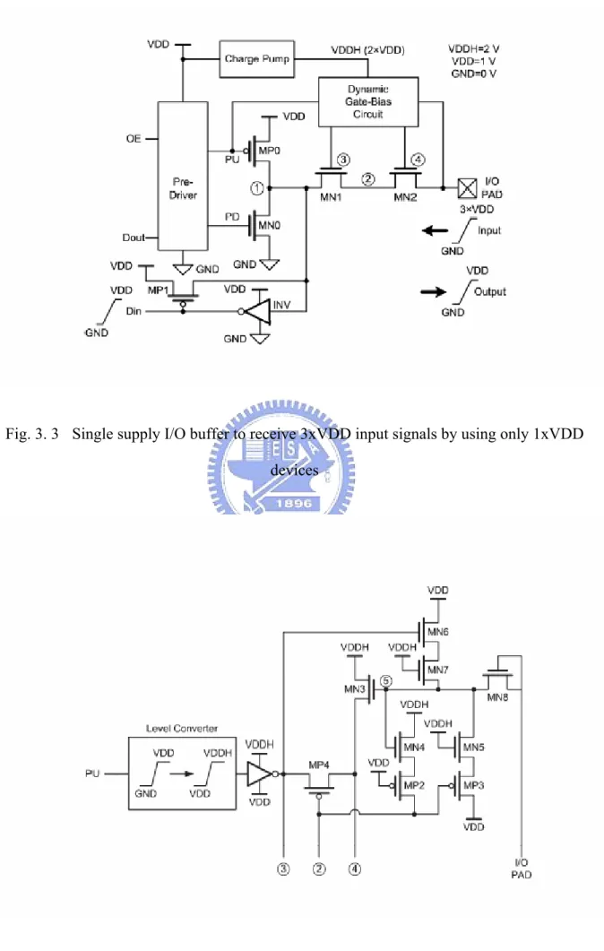
Fig. 3. 3 Single supply I/O buffer to receive 3xVDD input signals by using only 1xVDD devices ... 23
Fig. 3. 4 The circuit implementation of dynamic gate bias circuit using 1xVDD devices. ... 24
Fig. 3. 5 The proposed single supply SGO I/O driver with HVT input feature ... 26
Fig. 3. 6 Simulation waveforms of receiving mode ... 28
Fig. 3. 7 Simulation waveforms of transmitting mode... 28
Fig. 4. 1 The proposed dual power supply HVT SGO I/O output stage ... 34
Fig. 4. 2 The proposed dual power supply HVT SGO I/O input stage ... 36
Fig. 4. 3 The proposed dynamic bias circuit without static current at all operation modes ... 38
Fig. 4. 4 The proposed gate tracking circuit of dual supply SGO HVT I/O driver... 42
Fig. 4. 5 The proposed floating N-well tracking circuit ... 44
Fig. 4. 6 The proposed input buffer circuitry ... 47
Fig. 4. 7 The proposed input buffer circuitry with configured input threshold voltage ... 49
Fig. 4. 8 The input threshold voltage simulation results of configured input stage ... 50
Fig. 4. 10 Functional check waveforms of output mode simulation ... 53
Fig. 4. 11 Overstress check waveforms of output mode simulation... 54
Fig. 4. 12 Power current waveforms of output mode simulation ... 54
Fig. 4. 13 Functional check waveforms of input mode simulation ... 55
Fig. 4. 14 Overstress check waveforms of input mode simulation ... 56
Fig. 4. 15 Power current waveforms of input mode simulation ... 56
Fig. 4. 16 Functional check waveforms of HVT input mode simulation ... 58
Fig. 4. 17 Overstress check waveforms of HVT input mode simulation ... 59
Fig. 4. 18 Power current waveforms of HVT input mode simulation... 59
Fig. 4. 19 Functional check waveforms of output mode simulation at 500MHz ... 62
Fig. 4. 20 Overstress check waveforms of output mode simulation at 500MHz ... 63
Fig. 4. 21 Power current waveforms of output mode simulation at 500MHz ... 63
Fig. 4. 22 Functional check waveforms of HVT input mode simulation at 500MHz ... 64
Fig. 4. 23 Overstress check waveforms of HVT input mode simulation at 500MHz ... 65
Fig. 4. 24 Power current waveforms of HVT input mode simulation at 500MHz... 65
Fig. 4. 25 Functional check waveforms of under-drive output mode simulation at 133MHz... 67
Fig. 4. 26 Overstress check waveforms of under-drive output mode simulation at 133MHz... 68
Fig. 4. 27 Power current waveforms of under-drive input mode simulation at 133MHz 68 Fig. 4. 28 Functional check waveforms of under-drive input mode simulation at 133MHz ... 69
Fig. 4. 29 Overstress check waveforms of under-drive input mode simulation at 133MHz ... 70
Fig. 4. 30 Power current waveforms of under-drive output mode simulation at 133MHz ... 70
Fig. 4. 32 Overstress check waveforms of under-drive HVT input mode simulation at
133MHz... 72
Fig. 4. 33 Power current waveforms of under-drive HVT input mode simulation at 133MHz... 72
Fig. 4. 34 The cross section of deep N-well structure ... 73
Fig. 4. 35 Layout view of dual supply SGO HVT I/O driver... 74
LIST OF TABLES
Table2. 1 The truth table of input operation mode ... 9
Table2. 2 The truth table of output operation mode ... 9
Table3. 1 Operation modes of the proposed I/O circuitry... 24
Table3. 2 The static current at all operation modes... 28
Table3. 3 The cell delay and transition time of path I to PAD and path PAD to C ... 29
Table4. 1 Operation modes of the proposed I/O circuitry... 33
Table4. 2 The voltage table of dynamic bias circuit... 39
Table4. 3 The voltage table of gate tracking circuit at all operation modes... 42
Table4. 4 The voltage table of Floating N-well tracking circuit at all operation modes.. 46
Table4. 5 The bias table at each operation mode ... 51
Table4. 6 Simulation condition table... 52
Table4. 7 The cell delay and transition time of path I to PAD and path PAD to C. ... 57
Table4. 8 DC driving strength table ... 57
Table4. 9 The static current at all operation modes... 60
Chapter 1
Introduction
Conventional I/O buffers adopt both core devices and I/O devices to realize pre-decoding and post-decoding circuit blocks. The production needs more masks and process steps than base-line process. Single Gate Oxide (SGO) I/O buffer uses only core devices to achieve I/O function, and at least 4 masks including NLDD, PLDD, PW and NW of I/O devices can be saved to reduce manufacturing cost. Especially in the deep-submicron generation, the thickness of gate oxide has been scaled down to achieve higher speed performance and supply voltage also decreased [16] for lower power consumption. Only thin devices of CMOS technology are adopted to optimize speed, decrease manufacturing cost and simplify mask steps.
The penalty is the complexity of I/O circuitry to overcome the gate oxide reliability issues [10] and to prevent standby leakage current. Devices must be reliable for extended product lifetime. The targeted nominal lifetime is typically 5–10 years of continuous operation under specified worst-case operating conditions [4]. Three electric field strengths appear to be dominant for the lifetime of MOS transistors: the vertical and lateral electric field in the transistors and electric fields across junctions. The three lifetime-determining mechanisms corresponding to these fields are denoted as oxide breakdown [1], hot-carrier degradation [33], [3], and junction breakdown [8], respectively. The device reliability issue and traditional I/O driver design will be briefly discussed in chapter 2.
In chapter 3, the single supply SGO HVT I/O driver is presented. The I/O buffer realized with low-voltage devices and supplied with core voltage is capable of transmitting 1xVDD (core power) voltage levels but receiving 2xVDD input voltage levels without extra bias or charge bump circuit. Three prior arts are introduced in the chapter.
Nevertheless the SGO I/O buffers have the demand to drive peripherals with higher voltage than nominal core supply voltage. The new low power dual supply I/O buffer that uses only 1xVDD device to drive 2xVDD voltage and capable of tolerant 3xVDD input voltage is proposed in chapter 4. Three major circuit blocks including dynamic bias circuit, gate tracking circuit and floating N-well tracking circuit are proposed. They are also the most important innovation part of the thesis. Except product life time issue, low power and high performance are also the major challenges of SGO I/O driver design. Design technique and details are presented in this chapter.
Chapter 2
I/O Buffer Overview
2.1. Introduction
The reliability issue is the dominant factor of product life-time [1], [3]. Three main reliability issues are introduced in section 2.2, including the gate oxide reliability issue, hot-carrier degradation and junction breakdown.[4]
In section 2.3, two dual supply conventional I/O buffers are introduced. The regular I/O buffer and the conventional HVT I/O buffer with High Voltage Tolerant (HVT) input feature. The logic supply voltage or core voltage “VDD” is for logic base-band inside chips and the I/O supply voltage “VDDIO” is the output voltage level of I/O buffer to drive compatible standardized protocols. Most chips in advanced CMOS processes must be able to interface at voltages higher than their nominal supply voltage level. For example, 5V interfacing is required for ICs realized in processes with a nominal supply voltage of 3.3V. That is so-called high voltage tolerant (HVT) input I/O buffer.
A robust high-voltage-tolerant I/O which does not need process options is presented with Single Gate Oxide (SGO) I/O buffer. Only the core device is processed to reduce the manufacture cost. It also results to several problems. The I/O must be reliable for high yield and extended product lifetime. Except the main reliability concerns for the SGO I/O such as hot carrier injection degradation effects and time-dependent dielectric breakdown[5], [6],
[7], immunity from static current at all operation modes is required for reducing power consumption. In addition, I/O performance and AC characterization is very important in application. The I/O driver must have equal timing performance at each I/O level. This characteristic prevents board designers from being forced to retune the interface for optimal operation at each I/O level. The major challenges of single gate oxide I/O design are discussed in section 2.4.
2.2. Reliability Issues of I/O Buffer
Modern CMOS processes are optimized to get the maximum performance for the transistors used in ICs. Devices must be reliable for extended product lifetime. The targeted nominal lifetime is typically 5–10 years of continuous operation under specified worst-case operating conditions. Three electric field strengths appear to be dominant for the lifetime of MOS transistors: the vertical and lateral electric field in the transistors and electric fields across junctions. The three lifetime-determining mechanisms corresponding to these fields are denoted as oxide breakdown [1], [32], hot-carrier degradation [3], [33], and junction breakdown [8], respectively. These three mechanisms will be briefly discussed in the next parts of this section.
2.2.1. Gate Oxide Reliability
the device, if a certain amount of charge-per-area passed through the oxide. The oxide current, and hence the transistor’s lifetime, is a strong function of the applied electric field across the oxide. This value typically corresponds to a tolerable oxide voltage 20%~30% higher than the process’s nominal supply voltage [4].
At the source and drain sides of the transistor, the oxide voltage equals the source-gate voltage Vsg and the drain-gate voltage Vdg respectively. The oxide voltage
somewhere between the source and drain region is between Vsg and Vdg if the MOS
transistor is “on.” If the transistor is switched “off,” an applied bulk-gate voltage Vbg is
subdivided over a depletion layer in the silicon and over the gate oxide; the majority of the voltage falls across the depletion layer [4].
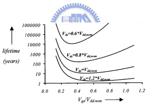
2.2.2. Hot-Carrier Degradation
With large drain–source voltages and transistors operating in saturation, carriers flowing from source to drain may gain high energies and become hot close to the drain region. Upon collisions with the silicon lattice, a small fraction of these hot carriers shoot into the gate oxide near the drain area, thereby slowly degrading the gate oxide and the transistor’s performance [3], [9], [28]. This so-called hot-carrier degradation effect depends among others on the transistor’s length and its biasing conditions [11]. The relation between the drain–source voltages and lifetime is exponential for deep submicron processes therefore their dependency is much close.
B
L
Tlife∝ where B= 1–5 [4] (2.1)
The relation between gate-source voltage and lifetime is more complex. For low gate-source voltages the transistor is “off” resulting in no current and hence in no hot carriers. For very high gate-source voltages (and fixed drain–source voltage) the transistor is in the linear region resulting in no hot carriers either. Somewhere in the middle, both the drain current is large and the transistor is well in saturation. In this region, the hot-carrier degradation is maximum and hence the lifetime is minimum [4].
Fig. 2. 1 Typical bias-lifetime behavior for minimum length MOS transistor
A typical hot-carrier-based lifetime versus biasing plot for a minimum length transistor is given in Fig. 2. 1 [4]; for longer transistors the lifetime is longer. The
2.2.3. Junction Breakdown
The third lifetime-threatening mechanism is junction breakdown [8]. For modern CMOS processes this junction breakdown occurs at voltages of at least a number of times the nominal supply voltage, therefore it is not a real concern for circuits. However, for reverse voltages somewhat higher than the nominal supply voltage, the junction goes into weak avalanche. With this effect, the reverse diode current, i.e., the leakage current increases with increasing reverse bias levels.
2.3. Conventional I/O Buffer Design Concept
The I/O buffer plays the role as interface between the chips and the peripherals in a system. They are the ports of chips to transmit or receive signal from other ICs. In order to interface chips with different supply voltage in a system, the I/O buffer must be able to tolerant higher voltage than its nominal power supply [12]. In the following sections, two I/O buffer design concepts are introduced. Note that this mixed voltage system may lead to several problems such as static leakage current and gate oxide reliability issue.
2.3.1. Regular I/O Buffer
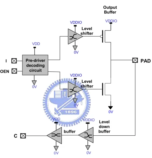
Conventional I/O buffer design concept diagram is presented as Fig. 2. 2. Input pin “OEN” controls the buffer to transmit (output) signals from “I” to “PAD” or to receive (input) signals from “PAD” to “C”. The level shifters level up signals from VDD to
transmit signal level of “PAD” to “C”. And the output buffer drives “PAD” with a specified driving strength. The truth tables of input operation and output operation are shown in Table2. 1 and Table2. 2 respectively.
I OEN VDD 0V Pre-driver decoding circuit PAD VDDIO 0V VDDIO 0V VDDIO 0V Level shifter VDDIO 0V VDDIO 0V Level shifter C Output Buffer Level down buffer
Fig. 2. 2 Regular I/O buffer block diagrams
The “VDD” is the nominal power supply for core device, and the “VDDIO” is the nominal power supply for I/O device. In mature technology, i.e. 0.25um process, the voltage level of VDD is biased at 2.5V, and VDDIO is supplied at the voltage of 5V. As
decreased to 1.0V in the typical low voltage 0.13-µm CMOS process and the I/O power voltage is still 3.3V for interfacing with mature peripherals [13].
output port OEN PAD I C 1 0 x 0 1 1 x 1 1 Z x x INPUT MODE input port
Table2. 1 The truth table of input operation mode
output port OEN I PAD 0 0 0 0 1 1 OUTPUT MODE input port
Table2. 2 The truth table of output operation mode
2.3.2. Conventional HVT I/O Buffer
The Conventional High Voltage Tolerant (HVT) I/O buffers basically have the same operation mechanism with regular I/O buffer introduced in previous section. The only one difference is the maximum tolerant voltage level of input stage. Some peripheral
components or other ICs are operated at higher voltage levels than I/O buffer’s nominal power supply of post decoder. For example, I/O buffers can output voltage level of 3.3V (I/O power) to drive peripherals but have to receive 3.3V or higher voltage, i.e. 5V from other chips in the system [29], [31]. This is so-called high voltage tolerant (HVT) input feature. Technological solutions can be pursued (e.g., multiple gate oxides [26]-[27]) which yield high-voltage-tolerant transistors at the cost of a more expensive process: masks and processing steps must be added to the baseline process.
The design concept diagram is presented as
Fig. 2. 3. When operation in High Voltage Tolerant (HVT) input mode, gate tracking circuit tracks the high voltage level of “PAD” to turn off output buffer PMOS to prevent static leakage current from “PAD” to “VDDIO”. Meanwhile, the floating N-WELL is charged to high voltage level. The MN1 levels down HVT input to ( VDDIO-Vt ) from PAD to prevent Vgd overstress of the lower cascade NMOS of output buffer. In the same
way, the MN2 levels down HVT input to ( VDDIO-Vt ) of PAD to protect the input stage buffers.
I OEN VDD 0V Pre-driver decoding circuit VDDIO 0V VDDIO 0V Level shifter VDDIO 0V VDDIO 0V Level shifter C Output Buffer VDD 0V buffer VDDIO 0V Level down buffer VDDIO 0V Gate Protection circuit VDDIO 0V Gate Protection circuit 0V VDDIO Floating N-well tracking circuit 0V VDDIO Floating N-well tracking circuit 0V VDDIO VDDIO PAD MN1 MN2 VDDIO float
Fig. 2. 3 Conventional HVT I/O buffer block diagrams
2.4. SGO I/O Buffer Overview
Both core devices and I/O devices are built in pre decoding and post decoding circuit blocks respectively of conventional I/O buffers. The production needs more masks and process steps than base-line process. Single Gate Oxide (SGO) I/O buffer uses only core devices to achieve I/O function [14],[30],and some innovative circuits are used to achieve high-voltage tolerance [20]-[25]. At least 4 masks including NLDD, PLDD, PW and NW of I/O device can be saved to reduce manufacturing cost. The penalty is the complexity of I/O circuitry to overcome the gate oxide reliability issues [10] and prevent standby leakage current. The voltages across all transistors’ terminals are carefully limited to sufficient low
values to ensure product lifetime at all operation modes.
2.4.1. Challenges of SGO I/O Buffer
2.4.1.1. Gate Oxide Reliability Issue
Generally speaking, minimum-length transistors operated at the nominal supply voltage will live at least the nominal lifetime. Higher stress results in shorter lifetime, lower stress results in longer lifetime. For MOS transistors, this stress usually corresponds to electric field strength in the device.
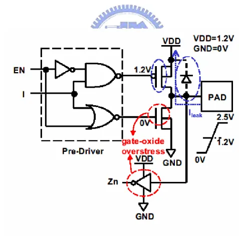
Single gate oxide (SGO) design uses only core device to tolerant high voltage of I/O power or high input voltage from the peripherals. For example, single supply I/O buffer using 1.2V device to tolerant 2.5V input voltage could be overstressed across Vgs ,Vgd ,Vgb
and even Vds as showninFig. 2. 4 [17]. Time-dependent-dielectric breakdown of thin gate
oxide is the main reliability concerns of SGO I/O design. More complicated circuit technique shall be applied to control stress across all CMOS terminals. Limitation of the electric fields is typically achieved at the cost of chip area. If a cost-efficient circuit implementation is also targeted, it is important not to design an overly robust circuit. Therefore knowledge of dominant lifetime-determining effects is essential in order to prevent both waste of chip area and to prevent insufficient lifetime [5][7].
2.4.1.2. Standby Leakage Current
An undesirable static current is induced once the voltage level of PAD is higher than power supply VDDIO about a diode turn-on voltage. Both PMOS and parasitic diode are turned on to lead to unexpected static current. This may happen when operation in HVT input mode as shown in Fig. 2. 4 [17]. Extra power consumption should be avoided to achieve low power design, especially in portable application.
Otherwise, circuitry with static current path at normal operation should be avoided to minimize power consumption.
Fig. 2. 4 Undesirable static current path and gate-oxide overstress when operation at HVT input mode.
2.4.1.3. Circuit Performance
Operation speed is the check point of circuit performance. In addition, the I/O driver must have equal timing performance at each I/O level. This characteristic prevents board designers from being forced to retune the interface for optimal operation at each I/O level. The I/O driver must drive capacitive loads at least 10 pF in low driving mode.
2.5. Conclusion
The reliability issues, design concerns and functions of I/O drivers are briefly introduced in this chapter. To design a reliable, low cost and high performance I/O driver is our target, and SGO design is exactly the low cost and high speed solution. The penalty is the complexity of I/O circuitry to overcome the gate oxide reliability issues and to prevent standby leakage current. It is important not to design an overly robust circuit to prevent waste of chip area. The design techniques will be presented in the following chapters.
Chapter 3
Single Supply SGO I/O with Input HVT Feature
3.1. Introduction
In the deep-submicron generation, the thickness of gate oxide has been scaled down to achieve higher speed performance and supply voltage also decreased [16] for lower power consumption application. The I/O buffer realized with low-voltage devices and supplied with core voltage can transmit 1xVDD (core power) voltage levels but receive 2xVDD input voltage levels without extra bias or charge bump circuit. The design concept and circuit implementation will be introduced in this chapter.
Three previous designs will be introduced in section 3.2. The prior art 1 and prior art 2 which are able to transmit 1xVDD voltage levels as well as receive 2xVDD input voltage levels use only thin gate oxide devices in implement. The prior art 3, a mixed-voltage I/O buffer designed with 1xVDD devices to receive 3xVDD input signals was reported [15]. The most advantage of the disclosure is that the input tolerant voltage level is up to three times core voltage VDD. However it only capable of driving 1xVDD voltage level and extra charge pump circuitry is needed.
In section 3.3, the proposed single supply SGO HVT I/O buffer is introduced. It achieves the same function as prior art 1 and prior art 2 but with reduced circuitry and layout area. Up to 30% reduction in floating N-well and gate tracking circuits compared to
prior art 2. Simulation results and circuitry implementation are presented in this section.
This chapter is introductory for Chapter 4. In next chapter, the reliable dual supply I/O buffer uses only 1xVDD device to drive 2xVDD voltage and capable of tolerant 3xVDD input voltage will be proposed.
3.2. Previous Design Overview
3.2.1. Prior Art 1
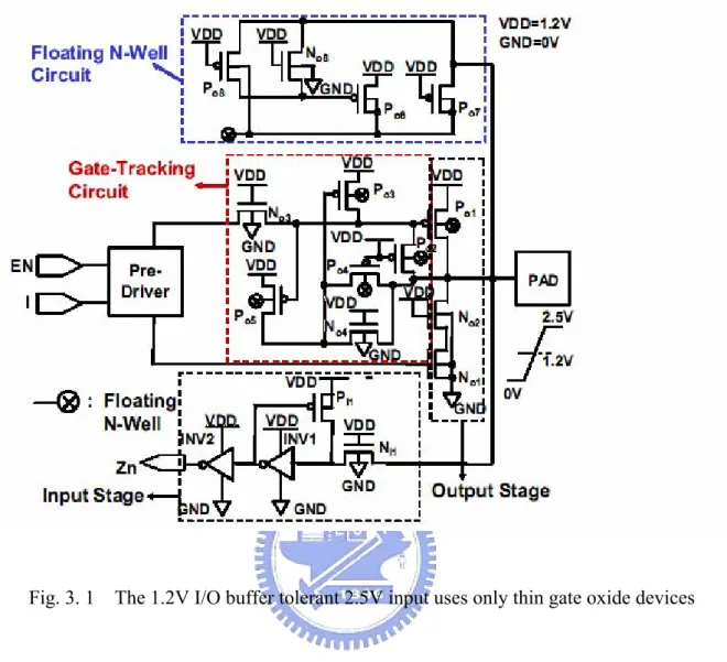
This 1.2V I/O buffer tolerant 2.5V input uses only thin gate oxide devices (1.2V devices) to realize I/O functions is shown in Fig. 3. 1 [17]. The operation description is as following.
When the I/O buffer is operated in the receiving mode, the upper and lower output ports of pre-driver will be 1.2V and 0V, respectively. The input signal coupled to pad for logic 0 is 0V, and for logic 1 is 2.5V. If the pad voltage is coupled to 2.5V, the PMOS devices Po7 and Po8 in the floating N-well circuit are turned on. Therefore, the PMOS Po6 is turned off for its gate voltage coupled to 2.5V through Po8, and the N-well voltage is coupled to 2.5V through Po7. On the other hand, Po2 and Po4 in the gate-tracking circuit are also turned on in this operating condition. Therefore, Po3 is turned off for its gate voltage coupled to 2.5V through Po4, and the gate voltage of Po1 is coupled to 2.5V
voltage is coupled to 0V, the gate voltage of Po6 is coupled to 0V through No8. Therefore, Po6 is turned on and the N-well voltage is kept at 1.2V through Po6. On the other hand, the gate voltage of Po3 is coupled to 0V through No4. Therefore, Po3 is turned on and the gate voltage of Po1 is coupled to 1.2V through Po3. With such arrangement, this I/O buffer can be correctly operating in the receiving mode in the mixed-voltage interface.
When the I/O buffer is operated in the transmitting mode, the upper and lower output ports of pre-driver will be controlled by the signal coupled to I, and the pad voltage is controlled by I. The input signal coupled to I for logic 0 is 0V, and for logic 1 is 1.2V. If the signal coupled to I is 0V, the two output ports of pre-driver are biased at 1.2V, and No1 of the output stage is turned on to kept the pad voltage at 0V. Therefore, the N-well and the gate voltages of Po1 in the output stage are kept at 1.2V by the floating N-well circuit and the gate-tracking circuit. If the signal coupled to I is 1.2V, the two output ports of pre-driver are biased at 0V, and Po1 is turned on to keep the pad voltage at 1.2V. In order to keep the gate voltage of Po1 at 0V exactly, Po5 is added to quickly turn off Po3 in this operating condition, where to avoid charging effect on the gate of Po1. On the other hand, the N-well voltage is kept at 1.2V because all the transistors in the floating N-well circuits are off without leakage path [17].
Fig. 3. 1 The 1.2V I/O buffer tolerant 2.5V input uses only thin gate oxide devices
3.2.2. Prior Art 2
Functions and specifications of this design [18] are similar to prior art 1 [17]. The most advantage of the disclosure is the reduced floating N-well circuit compared to prior art 1. The floating N- well is charged to VDDH through MP5 when the I/O driver is operated at high voltage tolerant mode. Except that it is charged only through parasitic diode and may not be charged to full VDD at normal transmitting and receiving modes. It is about the voltage level of (VDD-Vdiode). This is also the weakness of the I/O driver. The
The CMOS I/O buffer is shown in Fig. 3. 2 [18]. The left part is a pre-driver circuit and the other part is the main circuit. When OEN=“0” and the input signal DIN= “l”, the node “b” is discharged to 0V and the node “c” is also discharged to 0V. Therefore PAD voltage is pulled up to VDD by MP1 and MN2 is turned off. For the node “d” is discharged to 0V, the WELL voltage can be pulled up to VDD by MP6 via PAD. When the input signal DIN is “0”, the node “b” is initially pulled up to (VDD-Vt) and the node “c” is pulled up to VDD. Therefore, MN2 is turned on and the node “e” is discharged to 0V. So the node “b” can be pulled up to VDD to turn MP1 completely off. For the voltage level of node “d” is VDD, the WELL voltage can be pulled up to VDD by MP2.
When OEN= “l”, it is for input buffer use. It means that MP1 and MN2 are at off state. When the input high signal coupled to PAD is VDDH, the voltage of node “b” can be pulled up to VDDH by MP5 and the voltage of node “a” is pulled to (VDD-Vt). MP1 is turned off and MP4 is turned on to pull the voltage of node “e” to VDDH to keep MP3 off. The WELL voltage is pulled to VDDH by MP6 for the gate voltage of MP6 is coupled to VDD. Therefore, there are no leakage current paths and no gate-oxide overstress condition in all devices of the circuit. The “floating N-well” structure may lead to latch-up problem. Therefore, the double guard ring structure should be applied to avoid the issue [18].
Fig. 3. 2 The reliable and high voltage compatible CMOS I/O buffer
3.2.3. Prior Art 3
A mixed-voltage I/O buffer designed with 1xVDD devices to receive 3xVDD input signals was reported [15]. The most advantage of the disclosure is that the input tolerant voltage level is up to three times core voltage VDD. However it only capable of driving 1xVDD voltage level and extra charge pump circuitry is needed. The penalty of tolerant 3xVDD voltage input is the much more complicated circuitry and layout area.
(2V) of 2×VDD can be generated by an on-chip charge pump from VDD with 1×VDD devices[19]. Thus, the proposed I/O buffer can receive 3×VDD (3V) input signals without gate-oxide reliability issue by controlling the gate voltages of MN1 and MN2. The pre-driver can generate signals PU and PD to control the output transistors, MP0 and MN0. The protection devices, MN1 and MN2, are used to avoid high-voltage overstress. The dynamic gate-bias circuit controls the gate voltages of MN1 and MN2.
When the I/O buffer transmits a logic low (0V), the gate voltages of MN1 and MN2 are controlled at VDD, so the logic low can be transmitted from node 1 to the I/O pad. When the I/O buffer transmits a logic high (1V), the gate voltages of MN1 and MN2 are controlled at VDDH, so the logic high can be transmitted from node 1 to the I/O pad. When the I/O buffer receives a logic low (0V), the gate voltages of MN1 and MN2 are biased at VDD. Thus, the logic low signal can be transmitted to node 1 from the I/O pad. When the I/O buffer receives a logic high (3V), the gate voltages of MN1 and MN2 are biased at VDD and VDDH, respectively. In the 3×VDD receive mode, the voltage on node 2 (node 1) is pulled up to VDDH-Vt (VDD-Vt), where Vtis the threshold voltage of NMOS. Then, signal Din is pulled down to 0V to turn on MP1. Finally, the voltage on node 1 is fully restored to VDD, so the inverter INV has no DC leakage current. In this design, the gate-drain, gate-source, and drain-source voltages of every transistor do not exceed VDD. Thus, the I/O buffer with 1×VDD devices can tolerate 3×VDD input signals without gate-oxide reliability issue.
The dynamic gate-bias circuit is shown in Fig. 3. 4 [15]. In both transmit and receive modes, the signal PU has an inverting logic level of node 3. The voltage swing of signal PU is from GND (0V) to VDD (1V), but that of node 3 is from VDD (1V) to VDDH (2V).
Thus, a 0/1V-to-1/2V level converter followed by an inverter is used to generate the signal level of node 3 to control the gate of MN1. In the transmit mode, node 3 has the same signal level of node 4. Thus, nodes 3 and 4 are connected by MP4, whose gate is connected to node 2 to avoid the gate-oxide overstress. The voltage on node 5 must be biased at VDD and VDDH alternately in the transmit mode due to the gate-oxide reliability issue of MN3. When the I/O buffer transmits a logic low (0V), the gate voltages of MN1 and MN2 are kept at 1V, and MP3 is turned on to keep the voltage level on node 5 at VDD. When the I/O buffer transmits a logic high (1V), the gate voltages of MN1 and MN2 are kept at 2V, and MN6 is turned on to keep the voltage level on node 5 at VDD. The gate-drain and gate-source voltages of MN3 are always lower than 1V in the transmit mode, so there is no gate-oxide overstress issue on MN3.
The gate voltage (node 3) of MN1 is always kept at VDD in the receive mode. The gate voltage (node 4) of MN2 is controlled at VDD or VDDH by the input signal on the I/O pad. When the I/O buffer receives a logic high (3V), the voltage on node 5 is pulled up to the voltage level of 3×VDD-Vt through the diode-connected transistor MN8. At this
moment, MN3 and MN4 are turned on to pull the voltages on nodes 4 and 2 both up to VDDH. When the I/O buffer receives a logic low (0V), MP4 is turned on to pull the voltage on node 4 down to VDD, because the voltage on node 3 is VDD. At this moment, MP3 is turned on to pull the voltage on node 5 down to VDD to prevent the gate-oxide overstress on MN3. Besides, MP2, MN5, and MN7 can protect MN4, MP3, and MN6 against gate-oxide overstress.
Fig. 3. 3 Single supply I/O buffer to receive 3xVDD input signals by using only 1xVDD devices
Fig. 3. 4 The circuit implementation of dynamic gate bias circuit using 1xVDD devices.
3.3. The Proposed Single Supply SGO I/O Driver with HVT
Input Feature
3.3.1. Design Concept and Technique of the Proposed Circuit
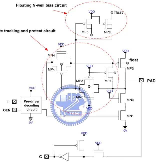
The proposed single gate oxide I/O driver with high voltage tolerant input feature saves up to 30% layout area of gate tracking and floating N-well dynamic bias circuits compared to prior art 1. The floating N-well is charged to the highest operation voltage levels at any modes to overcome the weakness in prior art 2. Totally four operation modes are listed in Table4. 1. VDD denotes the nominal power voltage, 1.2V and VDDHVP is the high tolerant input voltage, 2.5V. Two major circuit blocks: Gate tracking and protect circuit and dynamic floating N-well bias circuit are presented in Fig. 3. 5. The operation of input and output modes is described as below.
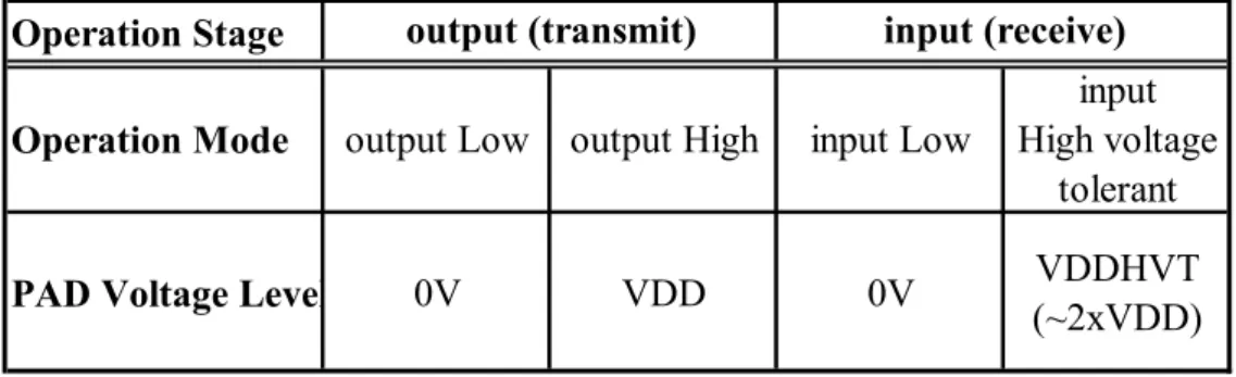
Operation Stage
Operation Mode output Low output High input Low
input High voltage
tolerant
PAD Voltage Level 0V VDD 0V VDDHVT (~2xVDD)
output (transmit) input (receive)
When OEN=1, the I/O buffer is operated at the receiving mode, and the upper and lower output ports of pre-driver will be 1.2V and 0V, respectively. If the pad voltage is coupled to 2.5V, the PMOS MP5 is turned off for its gate voltage coupled to 2.5V through MP3, and the N-well voltage is coupled to 2.5V through MP6. On the other hand, MP1 in the gate-tracking circuit is also turned on in this operating condition. Therefore, MP0 is turned off for its gate voltage coupled to 2.5V through MP1. Because the N-well and the gate voltages of MP0 are both coupled to 2.5V, there is no leakage path from pad to VDD when pad voltage is coupled to 2.5V. If the pad voltage is coupled to 0V, the gate voltage of MP5 is coupled to 0V through MN3. Therefore, MP5 is turned on and the N-well voltage is kept at 1.2V through MP5. On the other hand, the source side voltage of MP6 is coupled to 0V through MN3. Therefore, MP6 is turned off to prevent leakage path from floating N-well via MN3 to PAD. With such arrangement, this I/O buffer can be correctly operating at receiving mode.
When OEN=0, the I/O buffer is operated in the transmitting mode, and the upper and lower output ports of pre-driver will be controlled by the signal coupled to I. The input signal coupled to I for logic 0 is 0V, and for logic 1 is 1.2V. The PAD voltage is controlled by I. If the signal coupled to I is 0V, the two output ports of pre-driver are biased at 1.2V, and MN1 of the output stage is turned on to kept the PAD voltage at 0V. Therefore, the N-well and the gate voltages of MP0 in the output stage are kept at 1.2V by the floating N-well circuit and the gate-tracking circuit. If the signal coupled to I is 1.2V, the two output ports of pre-driver are biased at 0V, and MP0 is turned on to keep the PAD voltage at 1.2V. On the other hand, the N-well voltage is kept at 1.2V through MP5 for its gate voltage coupled to (VDD-Vt) through MN3. The parasitic diode composed by the drain side of MP0 and N-well helps to charge the N-well quickly. With such arrangement, this
I/O buffer can be correctly operating at transmitting mode. VDD VDD VDD VDD VDD VDD VDD VDD VDD VDD float 0V VDD VDD VDD VDD VDD VDD C float I OEN VDD 0V Pre-driver decoding circuit
3.3.2. Simulation Results
The circuitry is simulated with N65LP spice model in typical case at 25 . It drives ℃ capacitive loads of 30pF in PAD and 0.1pF in port C when operated at 300MHz sample rates. The nominal power supply VDD equals 1.2V and high voltage tolerant input VDDHVP equals 2.5V.
The function simulation waveforms of receiving and transmitting operation modes are illustrated in Fig. 3. 6 and Fig. 3. 7 respectively. It is verified successfully with N65LP spice model that the circuitry is immunity from static current at all operation modes as shown in Table3. 2.
Fig. 3. 6 Simulation waveforms of receiving mode
Fig. 3. 7 Simulation waveforms of transmitting mode
static cu rren t(A) I_ VDD
output 1.2V 3.34E-09
output 0V 4.18E-09
input 2.5V 4.70E-10
The timing checks of paths I to PAD at output mode and path PAD to C at input mode are well balanced as shown in Table3. 3.
Timing path rise_cell_delay rise_transition falling_cell_delay fall_transition I->PAD 9.28E-11 4.37E-11 9.61E-11 4.25E-11
PAD->C 1.35E-10 8.86E-11 1.41E-10 9.80E-11
Table3. 3 The cell delay and transition time of path I to PAD and path PAD to C
3.4. Conclusion
In this chapter, the I/O driver realized with low-voltage devices and supplied with core voltage can transmit 1xVDD (core power) voltage levels and receive 2xVDD input voltage levels is introduced and verified successfully with N65LP spice model. The proposed single gate oxide I/O driver with high voltage tolerant input feature saves up to 30% layout area of gate tracking and floating N-well dynamic bias circuits compared to prior art 1. The floating N-well is charged to the highest operation voltage levels at any modes to overcome the weakness in prior art 2. Nevertheless the demand of outputting higher voltage levels to drive the peripherals outside ICs is requested.
The I/O drivers with dual power supply and capable of outputting higher voltage levels ( I/O power) are the most popular I/O designs in modern semiconductor industry [2]. They are realized with both core devices and I/O devices practically. Extra mask steps, longer manufacture time and lower speed of I/O devices are suffered.
In next chapter, the low power consumption and high operation speed I/O drivers with dual power supply will be proposed. The reliable dual supply I/O buffer uses only 1xVDD device to drive 2xVDD voltage and capable of tolerant 3xVDD input voltage. That’s the new low power, high performance and low cost solution for I/O drivers.
Chapter 4
Dual Supply SGO I/O with Input HVT Feature
4.1. Introduction
Drivers with dual power supply are the most popular I/O design in modern semiconductor industry. The low voltage serves the base band area which contributes to the major part inside ICs to achieve low power consumption. Operation speed is also optimized for thinner gate oxide in deep-submicron technology. The high voltage supplies the I/O devices which are usually applied in analog modules and post-driver of I/O buffers. However the I/O devices suffer from lower speed for thicker gate oxide.
Only thin devices of CMOS technology are adopted to optimize speed, decrease manufacturing cost and simplify mask steps. Nevertheless the I/O buffers applied with only thin oxide still have to drive peripherals with high voltage and receive even higher voltage from other ICs. Gate oxide reliability, standby leakage current and circuitry performance are major challenges. The new low power dual supply I/O buffer that uses only 1xVDD device to drive 2xVDD voltage and capable of tolerant 3xVDD input voltage will be proposed in this chapter.
In section 4.2, the design concept and block diagram are introduced. The circuitry is divided into two major parts: output stage and input stage. The output stage transmits the logic level of input signal “I” to “PAD”. The input stage receives signals from “PAD” and
transmits its’ logic level to “C”. Major circuit blocks and their functions are described too.
The circuit implementation and design techniques are presented in section 4.3. Three major circuit blocks of output stage including dynamic bias circuit, gate tracking circuit and floating N-well tracking circuit are introduced. Two input stage circuits are proposed, and it’s a trade-off between layout area and performance. The overstress check is critically examined. Not only check gate oxide stress in steady state but also dynamically monitor the oxide stress condition in transient state. Simulation results of function, oxide stress and power consumption are presented too.
In section 4.4, layout of the I/O driver is implemented. The deep N-well structure is applied to isolate P-well with different potential. Guard rings and space between different N-wells should be carefully arranged to prevent latch-up problems.
In this chapter, the dual supply single gate oxide I/O driver with HVT input features circuitry is proposed. Three major challenges including gate oxide reliability issue, standby leakage of bias circuit and timing performance are solved and successfully verified with N65LP spice model.
4.2. Design Concept and Block Diagram
are presented in this section respectively.
Table4. 1 Operation modes of the proposed I/O circuitry
4.2.1. Output Stage
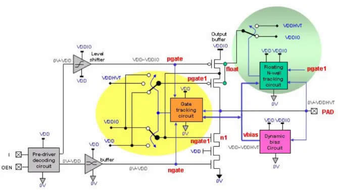
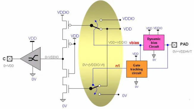
The block diagram of proposed dual power supply HVT SGO I/O output stage is illustrated in Fig. 4. 1. It is composed of pre-driver decoding circuit, buffer, level shifter, dynamic bias circuit, gate tracking circuit, output buffer stage, and floating N-well tracking circuit. Three major block; dynamic bias circuit, gate tracking circuit, and floating N-well tracking circuit will be emphasized in the following sections. All of them are supplied by core supply “VDD” or I/O supply “VDDIO”. The voltage level relations: VDDHVP=3xVDD, VDDIO=2xVDD.
Operation Stage
Operation Mode Output Low Output High Input Low Input High
Input High Voltage
Tolerant
PAD Voltage Level 0V VDDIO
(2XVDD) 0V
VDDIO (2XVDD)
VDDHVP (3xVDD)
Fig. 4. 1 The proposed dual power supply HVT SGO I/O output stage
Except operation at output “low” mode, the dynamic bias circuit senses the voltage level of “PAD” to output “vbias” between VDD~VDDHVT. Note that “vbias” presents a collection of various nodes including “bias”, “biasp”, and “biasl” which provide different voltage levels as shown in Fig. 4. 3. The generated bias voltage levels are fed to floating N-well tracking circuit and gate tracking circuit. According to the voltage levels received, these two circuit blocks will output control signals to switch the tracking levels. Only at output “low” mode, the dynamic bias circuit will be triggered by the gate tracking circuit and then feedback to the gate tracking circuit to work normally. It plays the role as the commander of the tracking and detecting system and doesn’t consume static current at all operation modes.
control signals and switch the voltage levels between VDD, VDDIO and VDDHVT to guarantee gate reliability of post decoder.
Floating N-well tracking circuit senses nodes of ”vbias”, ”pgate1” and “PAD” to dynamically control floating N-well voltage between VDDIO and VDDHVP. It charges the floating N-well of PMOS to the highest operation voltage to prevent leakage path of parasitic diode between PMOS drain side and N-well junction.
The biasing and tracking must be very fast in any state including the “transient state” in which the rise and fall times in the sub-nanosecond range may occur.
The level shifter transmits voltage level from 0~VDD to VDD~VDDIO. Previous design is adopted for circuit implementation.
4.2.2. Input Stage
The input stage receives the signals from port “PAD” and transmits its’ logic level to port “C”. The input logic high levels could be VDDHVP or VDDIO, and they would be leveled down to core voltage VDD for interfacing with internal core circuits. The block diagram is illustrated as Fig. 4. 2. The input stage shares the same dynamic bias circuit and gate tracking circuit with the output stage described in section 4.2.1. The “vbias” controls the switch of upper PMOS, and the signal “n1’ controls the switch of the second stack NMOS in the input buffer respectively.
Fig. 4. 2 The proposed dual power supply HVT SGO I/O input stage
4.3. Circuit Implementation
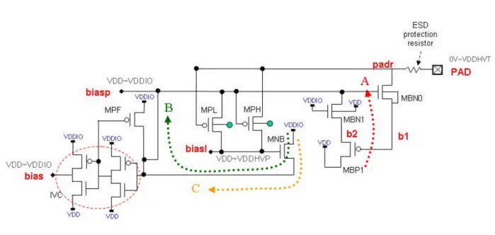
4.3.1. Dynamic Bias Circuit
In previous design, the biasing generation circuitry led to static leakage current and increased power consumption [7]. New bias method is proposed to provide bias levels for reliable and low power consumption operation. It senses the voltage level of “PAD” and dynamically feedback bias levels to other circuit blocks.
z The path A: When “PAD” =0V, pass VDD to “biasp”. The node “biasp” is charged to (VDD-Vt) through P-well of MBN1 to turn on MBN0. Then the node of “b1” is
coupled to 0V through MBN0 to turn on MBP1. Therefore the node “b2” is coupled to VDD through MBP1and the voltage level VDD is passed to “biasp” through MNB1. The voltage level VDD of “biasp” will fully turn on MBN0. The path A and MBN0 construct a positive feedback loop to charge the “biasp” to VDD when “PAD” =0V.
z The paths B: When “PAD”=VDDIO, pass (VDDIO-Vt) to “biasp”. It depends on the previous voltage level of “biasp” to decide the charge path. If its previous level is biased lower than (VDDIO-Vt), then “biasl” will be coupled to the voltage level of “PAD”, VDDIO, through MPH. Therefore MNB is turned on and “biasp” is pulled up to (VDDIO-Vt) through MNB. The path B is activated. Else if the voltage level of “biasp” is
higher than (VDDIO-Vt), it will be kept as VDDIO through positive feedback circuit “IVC” and “MPF”
z The path C: When “PAD” =VDDHVP, pass VDDIO to “biasp”. High voltage VDDHVP can pass MPH to turn on MNB, thus power supply voltage VDDIO is delivered to “biasp” through MNB.
z The inverter chain “IVC” speeds up “bias” to charge to VDD or VDDIO. It also works with MPF to positively feedback “biasp” to VDDIO.
z PMOS “MPL” passes voltage level of VDD to “biasl” to limit Vgd of MNB at (VDDIO-VDD) When “PAD” =0V.
z The P-well of MBN0 is connected to node “b1” to prevent junction breakdown when “PAD” =VDDHVP.
Fig. 4. 3 The proposed dynamic bias circuit without static current at all operation modes
The dynamic bias circuit detects the voltage level of “PAD” to generate respective bias levels which are fed to other circuit blocks for limiting the stress across Vgs,Vgd, Vds,
and Vgb. Only at output “low” mode, the dynamic bias circuit will be triggered by the gate
tracking circuit and then feedback to the gate tracking circuit to function normally. Typically, the stress value corresponds to a tolerable oxide voltage 20%~30% higher than the process’s nominal supply voltage [4]. The voltage table of dynamic bias circuit at all operation modes is shown in Table4. 2.
Node
PAD 0V VDDIO VDDHVP
biasp VDD VDDIO VDDIO
bias VDD VDDIO VDDIO
biasl VDD ~VDDIO VDDHVP
b1 0V VDDIO-Vt VDDIO-Vt
b2 VDD VDDIO-Vt VDDIO-Vt Voltage Level
Table4. 2 The voltage table of dynamic bias circuit
4.3.2. Gate Tracking Circuit
The signals “bias” and “biasp” generated by dynamic bias circuitry are fed to gate tracking circuit for gate protection. The gate tracking circuitry not only transmits logic levels to “PAD” but also protects output buffer stage not to be damaged by high voltage input (VDDHVP).The operation is described as following.
When the I/O buffer transmits a logic low (0V), the gate voltages of MON3 is controlled at VDD, and the node “pd” is biased at 0V to turn on MGP2 .So the node “pr” is coupled to VDD and then the voltage level of node “biasp” is coupled to (VDD-Vt) through MGN2 to turn on MON1. Therefore the logic low can be transmitted from ground through nodes n2 and n1 to the I/O port “PAD”. The dynamic bias circuit detects the voltage level 0V of “PAD”, and feedbacks a bias level as VDD to signal “bias” and pulls the voltage level of node “biasp” from (VDD-Vt) to full VDD. The MGN1 is turned on for its gate voltage level is coupled to VDD. The voltage level of node “pgate” is controlled at VDDIO to turn off MOP1. Then the voltage level of node “pgate1” is coupled to VDD through MGN3 to limit the stress between “pgate1” and “PAD” as VDD. The PMOS MGP1 is turned off for its Vsg=0V. Therefore the logic low can be transmitted to “PAD”
without static current and gate overstress.
When the I/O buffer transmits a logic high (VDDIO), the voltage level of node “pgate” is controlled at VDD to turn on MOP1. Then “bias” is coupled to VDDIO through
MOP1 to turn on MGN1. And the voltage level of node “pgate1” is coupled to VDD through MGN1 to turn on MOP2. Therefore the logic high (VDDIO) can be transmitted from I/O power supply VDDIO through MOP1 and MOP2 to the I/O port “PAD”. The dynamic bias circuit detects the voltage level “VDDIO” of “PAD”, and feedbacks a bias level as VDDIO to signal “biasp” to turn off MGP1 and MGN3 and turn on MON1. The voltage level of node “n1” is coupled to (VDDIO-Vt) through MON1 and leveled down to (VDD-Vt) through MON2 at node “n2”. The gate voltage of MON3 is controlled at 0V, and the node “pd” is biased at VDD to turn off MGP2. The NMOS MGN2 blocks voltage level “VDDIO” of node “biasp” to protect MGP2. Meanwhile the voltage level of node “pr” is coupled to near VDD. Therefore the logic high can be transmitted to “PAD” without static current and gate overstress.
When the I/O buffer receives a logic low (0V), the voltage levels of node “ngate” and “pgate” are controlled at 0V and VDDIO respectively to turn off MON3 and MOP1. And the node “pd” is controlled at VDD to turn off MGP2. The dynamic bias circuit detects the voltage level 0V of “PAD”, and generates a bias level as VDD to signals “biasp” and “bias”. Therefore the node “pgate1” is coupled to VDD through MGN3 to limit the Vgd of
MOP2 at VDD. The NMOS MON1 is turned on because its gate voltage level is charged to VDD. The node “n1” is coupled to 0V through MON1 and the node “n2” is coupled to 0V through MON2. Therefore, there are no leakage current paths and no gate-oxide overstress condition in all devices of the circuit.
circuit detects the voltage level VDDHVP of “PAD”, and feedbacks a bias level as VDDIO to signals “biasp” and “bias”. Therefore the node “pgate1” is coupled to VDDHVP through MGP1 to turn off MOP2. MGN1 and MGN3 are turned off for their Vgs=0V. The node
“n1” is coupled to (VDDIO-Vt) through MON1 and leveled down to (VDD-Vt) at node “n2” through MON2 to protect MON3. MGN2 blocks VDDIO of node “biasp” to protect MGP2. The P-well of MON1 is connected to node “n1” to prevent junction breakdown when “PAD” =VDDHVP.
When the I/O buffer receives a logic high (VDDIO), the voltage levels of node “ngate” and “pgate” are controlled at 0V and VDDIO respectively to turn off MON3 and MOP1. And the node “pd” is controlled at VDD to turn off MGP2. The dynamic bias circuit detects the voltage level VDDIO of “PAD”, and feedbacks a bias level as VDDIO to signals “biasp” and “bias”. Therefore the node “pgate1” is coupled to (VDDIO-Vt) through MGN1 and MGN3. MGP1 is turned off for its Vsg=0V. The node “n1” is coupled to
(VDDIO-Vt) through MON1 and leveled down to (VDD-Vt) at node “n2” through MON2 to protect MON3. MGN2 blocks VDDIO of node “biasp” to protect MGP2. Therefore, there are no leakage current paths and no gate-oxide overstress condition in all devices at high voltage input mode.
Fig. 4. 4 The proposed gate tracking circuit of dual supply SGO HVT I/O driver
The voltage table of gate tracking circuit at all operation modes is shown in Table4. 3.
Mode Output 0V Output VDDIO Input 0V Input VDDIO Input VDDVT
pagate VDDIO VDD VDDIO VDDIO VDDHVP
bias VDD VDDIO VDD VDDIO VDDIO
pagate1 VDD VDD VDD VDDIO-Vt VDDHVP
biasp VDD VDDIO VDD VDDIO VDDIO
biasl VDD ~VDDIO VDD ~VDDIO VDDHVP
PAD 0V VDDIO 0V VDDIO VDDHVP
n1 0V VDDIO-Vt 0V VDDIO-Vt VDDIO-Vt
n2 0V VDD-Vt 0V VDD-Vt VDD-Vt
4.3.3. Floating N-well Tracking Circuit
To prevent undesirable static current flowing through the parasitic diode composed by the drain oxide and N-well junction of the PMOS, the voltage level of floating N-well must be higher than the voltage level of its source or drain. The proposed floating N-well tracking circuit dynamically tracks a proper voltage level in response to the voltage level of “PAD”. When I/O circuitry is operated at high voltage tolerant input mode, the floating N-well is charged to high voltage VDDHVP. Otherwise it tracks the I/O power voltage VDDIO.
The tracking circuit also suffers from gate oxide overstress issue. The node voltage should be biased well at all operation modes. The floating N-well tracking circuit is proposed as Fig. 4. 5.
Fig. 4. 5 The proposed floating N-well tracking circuit
Three main voltage tracking paths and the circuit operation are described as following:
z The path A: It is the floating N-well bias path when the I/O driver operates at all output modes and at input “low” mode. The node “pgate1” is biased at VDD when operation at all output modes and at input “low” mode. Therefore the PMOS MWP5 is turned on and VDDIO is coupled to node “float”. When it is operated at input VDDIO mode, the voltage level of node “pgate1” is (VDDIO-Vt) and MWP5 may not be turned on.
high mode.
z The path B: VDDHVP can be passed to floating N-well when the I/O driver operates at HVT input mode. The node “bias” is coupled to VDDIO when operation at HVT input mode to turn on MWP2. The node “float” is coupled to VDDHVP through MWP2 and MWP1. Meanwhile the nodes “pgate1” and “fg” are coupled to VDDHVP to turn off MWP5 and MWP4 respectively. Therefore no standby current flows to VDDIO when operation at HVT input modes.
z The path C: It is only disabled when operation at HVT input mode and enabled at all nominal input and output modes. The voltage level of node “fg” is coupled to VDDHVP to turn off MWP4 at HVT input mode. This can prevent static current flowing to VDDIO through MWP4. The node “fg” is coupled to ~VDD at all nominal input and output modes. Therefore the node “float” is coupled to VDDIO through MWP4. This path is enabled especially at input “high” (VDDIO) mode to assist path A.
z The bias node “biasl”: Connect drain side of MWP2 to“biasl” to limit the Vds of MWP2= VDD when “PAD"transients from VDDHVP to 0V
When the I/O driver operates from HVT input into VDDIO input mode, the float N-well will discharge from VDDHVP to VDDIO slowly through junction leakage path if the PMOS MWP5 is not fully turned on. It neither disturbs normal function nor contributes side effects to gate reliability issue. To discharge rapidly can be achieved by tying PAD to 0V first to reset the N-well potential.
Table4. 4 The voltage table of Floating N-well tracking circuit at all operation modes
4.3.4. Input Stage
Two input stage circuits are proposed. The first input buffer circuitry has simpler circuitry and about 30% smaller layout area compared to the second proposal. But its threshold voltage can not be biased at half VDDIO when the circuitry operates at input high mode. The second proposal with configured input threshold voltage solves the problem but occupied larger layout area
4.3.4.1. Input Buffer Circuitry
The input buffer circuit implementation is illustrated in Fig. 4. 6, and described as following:
z The NMOS “MN1” levels down voltage level of “PAD” from VDDHVP to
Mode Output0V VDDIOOutput Input0V VDDIOInput VDDHVTInput
bias VDD VDDIO VDD VDIO VDDIO
pagate1 VDD VDD VDD VDDIO-Vt VDDHVP
biasl VDD ~VDDIO VDD ~VDDIO VDDHVP
fg ~VDD ~VDD ~VDD ~VDD VDDHVP
z The NMOS “MND” levels down the voltage level of node “nc” from (VDDIO-Vt)
to (VDD-Vt) to prevent overstress between Vgs and Vgd of MN1.
z The PMOS “MPU” pulls up node “cb” from (VDD-Vt) to full VDD.
z It’s unable to bias the input threshold voltage at 1/2xVDDIO. The Vth of the
proposed input buffer circuitry without threshold configured is about 1/2xVDD.
Fig. 4. 6 The proposed input buffer circuitry
4.3.4.2. Input Buffer Circuitry with Configured Threshold Voltage
Proposed input buffer circuitry with configured input threshold voltage is illustrated in Fig. 4. 7. The Vth of the proposed circuitry is biased at 1/2xVDDIO. The operation is
described as following:
The input signal coupled to pad for logic 0 is 0V, and for logic 1 is VDDIO and VDDHVP. Signals “bias” and “n1” are fed by dynamic bias circuit and output buffer stage introduced in previous section. When the circuitry is operated at input HVT mode, the pad voltage is coupled to VDDHVP, and the node “bias” is coupled to VDDIO to turn off MIP1. The voltage level of node “n1” is coupled to (VDDIO-Vt) to turn on MIN5 and transmit VDD to node “np” to turn on MIN2. Therefore the voltage level of node “nc” is coupled to 0V and propagated to node “cb” to turn on MIP3. The voltage level of node “c1” is coupled to VDD through MIP3 and propagated to port “C”. The same operation when the voltage of “PAD” is coupled to VDDIO.
When the circuitry is operated at input low mode, the pad voltage is coupled to 0V, and the node “bias” is coupled to VDD to turn on MIP1. The voltage level of node “n1” is coupled to 0V to turn off MIN5 and transmit to node “np” through MIN4 to turn off MIN2. Therefore the voltage level of node “nc” is coupled to VDDIO through MIP1 and MIP2 and leveled down to (VDD-Vt) through MND. Thus the node of “cb” is coupled to (VDD-Vt) to turn on MIN3. The node “c1” is pulled down to 0V through MIN3 and meanwhile the PMOS MIP3 is slightly turned on for its gate voltage level is (VDD-Vt). The PMOS MPU is turned on to pull up the voltage level of node “cb” to full VDD and turn off MIP3 completely. Finally the voltage level of 0V is propagated to port C.
z The NMOS “MIN4” and “MIN5” level down voltage of “n1” from 0 ~ (VDDIO-Vt) to 0 ~ (VDD-Vt) to avoid overstress between neighbor gate oxides.
z The NMOS “MND” levels down VDDIO to VDD to guarantee the gate reliability of the next stage.
z The PMOS “MPU” pulls up node “cb” from (VDD-Vt) to full VDD.
z The input threshold voltage is configured at 1/2xVDDIO for wider noise margin. Simulation waveform is shown in Fig. 4. 8.
z The node “bias” swings from VDD~VDDIO is fed from dynamic bias circuit.
z The node “n1” is fed from the output buffer stage of post driver as shown in Fig. 4. 1.
Fig. 4. 8 The input threshold voltage simulation results of configured input stage
4.3.5. Bias Check
The bias levels of major nodes at each operation mode are listed in Table4. 5. Overstress check of gate oxide reliability is presented as control path matrix as shown in Fig. 4. 9. Arrows denote the dependency of the control path. Stress conditions of all the control paths are checked by simulator to guarantee gate oxide reliability no matter operation in steady or transient state.
PAD
Mode Output 0V Output VDDIO Input 0V Input VDDIO Input VDDVT
pagate VDDIO VDD VDDIO VDDIO VDDHVP
bias VDD VDDIO VDD VDDIO VDDIO
pagate1 VDD VDD VDD VDDIO-Vt VDDHVP
biasp VDD VDDIO VDD VDDIO VDDIO
biasl VDD ~VDDIO VDD ~VDDIO VDDHVP
PAD 0V VDDIO 0V VDDIO VDDHVP
n1 0V VDDIO-Vt 0V VDDIO-Vt VDDIO-Vt
n2 0V VDD-Vt 0V VDD-Vt VDD-Vt
ngate VDD 0V VDD 0V 0V
float VDDIO VDDIO VDDIO VDDIO VDDHVP
Table4. 5 The bias table at each operation mode
4.3.6. Simulation Results
The dual supply single gate oxide I/O driver with HVT input features circuitry is simulated with N65LP spice model in typical case at 25℃. It drives capacitive loads of 30pF in PAD and 0.1pF in port C and is operated at 300MHz sample rate. Supply voltage levels are listed as following: The core supply VDD=1.2V, I/O supply VDDIO=2.5V and high voltage tolerant input VDDHVP=3.6V. The specifications are summarized in Table4. 6. N65LP TT / 25℃ 300MHz VDD 1.2V VDDIO 2.5V VDDHVP 3.6V PAD 30pF C 0.1pF Spice Model Loading Case / Temp. Simulation Speed Supply Levels
Table4. 6 Simulation condition table
The functional check, overstress check and power current waveforms of output mode simulation are illustrated respectively in Fig. 4. 10, Fig. 4. 11, and Fig. 4. 12. The overstress check includes all control paths which have been introduced in previous section as bias check matrix (Fig. 4. 9). The stress levels should be operated less than 1.56V
The same functional check, overstress check and power current waveforms of nominal input mode simulation are presented respectively in Fig. 4. 13, Fig. 4. 14, and Fig. 4. 15. The received voltages of PAD swing from 0V up to 2.5V and level down to 1.2V in port C.
The timing checks of paths I to PAD at output mode and path PAD to C at nominal input mode are well balanced as shown in Table4. 7. DC driving strength table is shown as Table4. 8.
Timing Path (S) rise_cell_delay rise_transition fall_cell_delay fall_transition I->PAD 3.26E-10 1.38E-10 3.22E-10 1.26E-10
PAD->C 2.07E-10 8.35E-11 2.26E-10 8.06E-11
Table4. 7 The cell delay and transition time of path I to PAD and path PAD to C.
Parameter Driving Strength (A) Ioh @ Voh=1.7V 1.49E-02
Iol @ Vol=0.7V 1.27E-02
Table4. 8 DC driving strength table
The simulation waveforms of functional check, overstress check and power current at HVT input operation mode are presented respectively in Fig. 4. 16, Fig. 4. 17, and Fig. 4. 18. The voltage level of HVT input up to 3.6V is leveled down to 1.2V before propagating to internals of ICs.
Fig. 4. 17 Overstress check waveforms of HVT input mode simulation