i
國 立 交 通 大 學
電子工程學系 電子研究所碩士班
碩 士 論 文
射頻金氧半場效電晶體之元件佈局對高頻
特性與低頻雜訊之影響以應用於
射頻與類比電路
RF MOSFET Layout Effect on
High Frequency Characteristics and
Low Frequency Noise for RF and Analog
Circuit Applications
研 究 生:古智友
指導教授:郭治群 博士
i
射頻金氧半場效電晶體之元件佈局對高頻特性與
低頻雜訊之影響以應用於射頻與類比電路
RF MOSFET Layout Effect on High Frequency
Characteristics and Low Frequency Noise
for RF and Analog Circuit Applications
研究生: 古智友 Student : Chih-You Ku
指導教授:郭治群 博士 Advisor : Dr. Jyh-Chyurn Guo
國 立 交 通 大 學
電子工程系 電子研究所
碩 士 論 文
A Thesis
Submitted to Department of Electronics Engineering & Institute of Electronics
College of Electrical Engineering and Computer Science
National Chiao Tung University
in partial Fulfillment of the Requirements
for the Degree of Master
In
Electronics Engineering September 2010
Hsinchu, Taiwan, Republic of China
i
射頻金氧半場效電晶體之元件佈局對高頻特性
與低頻雜訊之影響以應用於射頻與類比電路
學生:古智友 指導教授: 郭治群 博士
國立交通大學 電子工程學系 電子研究所碩士班
摘要
本論文主要是探討元件佈局造成的 STI 應力,和經由 STI 製程頂邊所產生的圓角 TCR(Top Corner Rounding)與隨之而來的W 效應對直流 I-V 特性、電導(Gm),以及載子遷移
率(eff)的影響。同時我們也分析此兩種機制對元件低頻雜訊與高頻特性所產生的影響。
為了提高的 STI 垂直方向的應力,我們設計了狹窄型 OD 和多重 OD MOSFETs 兩種元 件,其概念是由標準多指元件(Standard multi-finger MOSFETs)延伸而來的。而維繞式 MOSFET 是我們所設計的另一種全新結構,它在從垂直方向完全不受到 STI 應力影響,
關鍵就是在於它完全在 width 方向避開了的 STI/OD 界面,並藉此改善低頻雜訊。 但是 在某些元件的量測結果顯示,我們無法從 STI 的應力解釋在極端狹窄的元件的反而有更 低的低頻雜訊。因次我們從 STI 頂邊 TCR 導致的W 的角度去分析,推導出一
semi-empirical 模型,能夠模擬以預測 width 微縮對eff 與 Gm之影響,藉由這些模型可
以準確的求出有效的通道寬度 Weff。 STI 應力愈強將導致介面缺陷電荷(Nit)的增加,但
是此效應確遠不及W 明顯,對於狹窄型元件來說是一項優點。但不幸的是狹窄型元件
的截止頻率還是會因為 Cgg 增加而下降,而且無法經由去寄生的方式改善。
在低頻雜訊與高頻特性之間有著權衡的 RF 元件佈局設計考量。因此基板接點的元件 設計是一個有趣的課題,我們設計各種基板接點結構的 4-port 測試元件並將基板端獨
ii
立接出來,將我們提出新的 body network 模型萃取元件參數如基板電阻,它影響高頻元 件特性與低頻雜訊特性。量測結果顯示愈大的基板電阻會產生愈大的低頻雜訊,我們可 以藉由多重環狀佈局的方式設計基板接點形狀,藉此大量降低基板電阻,但同樣地此舉 也會使閘極至基板接點間的雜散電容增加而降低截止頻率。
iii
RF MOSFET Layout Effect on High Frequency
Characteristics and Low Frequency Noise for
RF and Analog Circuit Applications
Student:Chih-You Ku Advisor:Dr. Jyh-Chyurn Guo
Department of Electronics Engineering Institute of Electronics
National Chiao Tung University
Abstract
The impact of layout dependent STI stress and W from STI top corner rounding (TCR) on I-V characteristics, transconductance (Gm), effective mobility (eff), low frequency noise
(LFN), and high frequency performance has been investigated in this thesis. Narrow-OD and
multi-OD MOSFETs are two structures derived from standard multi-finger MOSFET for
enhancing transverse stress ⊥. Donut MOSFET is another structure created to keep free from
⊥, due to the elimination of STI/OD boundary along the channel width direction.
The compressive stress from STI cannot explain the lower LFN in extremely narrow
devices. STI top TCR induced W is identified as an important factor responsible for the
increase of Gm and the reduction of LFN with width scaling to nanoscale regime. A
semi-empirical model was derived to simulate eff degradation from STI stress and the
increase of effective width (Weff) from W. The proposed model can accurately predict width
scaling effect on Gm based on a trade-off between eff and Weff. The enhanced STI stress may
lead to an increase of interface traps density (Nit) but the influence is relatively minor and
overcome by Weff effect. Unfortunately, the extremely narrow devices suffer fT degradation
iv
deembedding. The trade-off between LFN and high frequency performance provides an
important layout guideline for analog and RF circuit design.
Body contact layout effect on LFN and high frequency performance is one more
interesting topic of research in this thesis. Four-port test structures were implemented to
accommodate 4-terminal MOSFETs with separate body terminal and a new body network
model has been developed to simulate the body contact layout and body biases effects. The
measurement result reveals that the higher body resistance will lead to the worse LFN
characteristic. We can significantly reduce the body resistance by applying multi-ring body
contacts, but this may contribute larger parasitic capacitance from poly gate to body contacts
v
誌謝
首先,我要感謝我的指導教授--郭治群教授。在研究方法及態度上的指導,不斷地 替學生尋找研究資源,並且嚴格要求學生完成許多基礎工作。在這過程中,除了建立許 多研究領域相關的能力,在國際學術會議及期刊發表論文,也體會到許多待人接物的觀 念,相信將會成為我未來工作上或者研究上的準則。 此外,還要感謝 NDL 的研究員—黃國威博士,在研究設備上的支持,讓我能夠接 觸並學習到高頻量測設備。也感謝 RFTC 的工程師們,邱佳松、林書毓、蕭治華在量測 實驗上的協助以及建議,讓我能夠順利完成量測。 感謝 LAB635 中的所有成員們,國良學長、冠旭學長、依修學長、仁嘉學長在研 究上的幫忙,也感謝敬文、弈岑、唯倫、智翔、德昌的陪伴 ,讓我在實驗室的生活更 豐富有趣。 最後,我要感謝一直在背後支持我的家人,他們在我求學與成長的路上付出許多。vi
Contents
Chinese Abstract
...iEnglish Abstract
...iiiAcknowledgement
...vContents
...viFigure Caption
...ixTable Caption...xvii
Chapter 1 Introduction
1.1 Research Motivation...11.2 Thesis Organization...2
Chapter 2 Low Frequency Noise Theory and Measurement Method
2.1 An Overview of CMOS Technology and Low Frequency Noise...42.2 Low Frequency Noise Theory...8
2.2.1 Number Fluctuation Theory...9
2.2.2 Mobility Fluctuation Theory...10
2.3 Low Frequency Noise Measurement System...12
2.4 Low Frequency Noise Data Analysis Method...18
Chapter 3 Analysis of Layout Effect on STI Stress and Device Parameters
3.1 STI Stress Mechanics in RF MOSFET...233.2 MOSFET Layouts for STI Stress Modulation (Multi-finger, Multi-OD, and Doughnut Structures) ...25
3.3 Layout Effect on DC Characteristics...27
3.4 STI Top Corner Rounding (TCR) Effect on Weff and Gm...36
3.5 STI Top Corner Rounding (TCR) Technique – Stress and W...38 3.6 C-V Characterization and Fringing Capacitances Simulation for Accurate
vii
Mobility Extraction...40
3.6.1 Open Deembedding Methods for Intrinsic Cgg Extraction...40
3.6.2 3-D Fringing Capacitances Simulation and Analysis using Raphael...45
3.6.3 Effective Mobility Extraction for MOSFETs with Various Layouts...51
3.7 CP Current Measurements for Interface States Extraction and Analysis of STI Stress Effect...58
Chapter 4 RF MOSFET Layout effect on Low Frequency Noise
4.1 Low Frequency Noise Analysis in Two-port 3T MOSFET...614.2 Narrow-OD MOSFET and Comparison with Standard MOSFET...61
4.3 Multi-OD MOSFET and Comparison with Standard MOSFET1...63
4.4 Doughnut MOSFET and Comparison with Standard MOSFET...66
4.5 Comparison between NMOS and PMOS...68
4.6 Layout Dependence of Interface States and Low Frequency Noise...70
4.7 Low Frequency Noise Model Parameter Extraction for Simulation...74
Chapter 5 RF MOSFET Layout Effect on High Frequency Characteristics
5.1 Two-port S-parameters Measurement and Deembedding...765.2 Two-port 3T MOSFET with Multi-finger, Multi-OD, and Doughnut Structures....77
5.2.1 Intrinsic Device and Parasitic RLC Parameters Extraction and Analysis – Layout Effect and Bias dependence...78
5.2.2. High Frequency Performance Analysis (fT, fMAX, NFmin)...83
5.3 Four-port 4T MOSFET with Various Body Contact Layouts...93
viii
5.3.2 Intrinsic Device and Parasitic RLC Parameters Extraction and Analysis – Body Contact Layout Effect and Bias dependence...97
Chapter 6 Conclusion
6.1 Summary...102 6.2 Future Work...103
ix
Figure Captions
Chapter 2
Fig.2.1 Schematical illustration of phase noise spectrum in VCO...7
Fig.2.2 Schematical illustration of electrons in the channel of MOSFET moving in and out of
the traps giving rising to fluctuations in the inversion carrier density and thereby the drain current...10
Fig.2.3 Schematic of SR570 flicker noise measurement system setup with SR570 LNA
(trans-resistance amplifier), Agilent DSA 35670 (dynamic signal analyzer), and HP4142B (DC power supply)...14
Fig.2.4 Schematic of low frequency noise measurement system consisting of model 5184
LNA (voltage amplifier), HP4142B for DC supply, and Agilent 35670 for dynamic signal analyzer...16
Fig.2.5 New solution for using model 5184 LNA (a) Battery (b) ultra low noise DC source
(PA14A1) as a power supply...16
Fig.2.6 Schematic illustration of Celestry 9812B Noisepro system consisting of HP4145 for
DC supply, 9812B for pre-amplifier, and Agilent 35670 for dynamic signal analyzer...17
Fig.2.7 Normalized PSD of drain current noise SID/IDS2 measured from (a) NMOS and (b)
PMOS with increasing frequency, under various VGT (|VGT |=0.1, 0.3, and 0.5V). NMOS and
PMOS fabricated in 90nm low leakage process...21
Fig.2.8 Normalized PSD of drain current noise SID/IDS2 measured from (a) NMOS and (b)
PMOS under increasing |VGT| and fixed |VDS|=0.05V. ...22
Fig.2.9 Normalized PSD of drain current noise SID/IDS2 versus frequency, measured from (a)
NMOS and (b) PMOS under |VGT|=0.3V and |VDS|=0.05V. NMOS and PMOS were fabricated
in 90nm low leakage CMOS process...22
Chapter 3
x
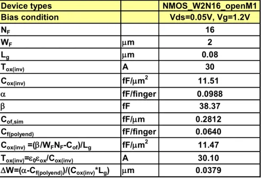
Fig.3.2 Schematics of narrow-OD MOSFETs with three layouts (a) W2N16 (WF×NF=2m×16)
(b) W1N32 (WF× NF=1m × 32) (c) W05N62 (WF× NF=0.5m × 64) corresponding to
Wtot=32m...26
Fig.3.3 Schematics of multi-OD MOSFETs with three layouts (a) OD1 (WOD × NOD=2m×1)
(b) OD8 (WOD × NOD=0.25m×8) (c) OD16 (WOD×NOD=0.125m×16)...26
Fig.3.4 A brief layout of donut MOSFET with two major layers, such as active region (OD)
and poly gate (PO) (a) D1S1 (poly gate to STI edge distance =0.3m (min. rule) (b) D10S10 (poly gate to STI edge distance =3m=10x min. rule), 4-side polygons length is 16 m x4...27
Fig.3.5 Schematics of STI stresses along the longitudinal and transverse directions, defined as
// and ⊥ in MOSFETs with different layouts (a) standard multi-finger MOSFET (b)
narrow-OD MOSFET...30
Fig.3.6 Linear VT versus WOD for narrow-OD NMOS with various layouts like W2N16
(WOD=2m, NF=16), W1N32 (WOD=1m, NF=16), W05N64 (WOD=0.5m, NF=16) under the
biases of VDS=50mV and VBS=0V...31
Fig.3.7 (a) The drain current IDS vs. VGT (b) transconductance Gm vs. VGT measured from
narrow-OD NMOS W1N32 (WF=1m, NF=32) and W05N64 (WF=0.5m, NF=64), and
standard multi-finger NMOS W2N16 (WF=2m, NF=16). All of the devices have the same
total finger width, WF×NF=32m...32
Fig.3.8 Schematics of STI stresses along the longitudinal and transverse directions, defined as
// and ⊥ in MOSFETs with different layouts (a) standard multi-finger MOSFET (b)
multi-OD MOSFET with multiple OD finger and multiple gate finger...32
Fig.3.9 Linear VT versus WOD for multi-OD NMOS with various layout dimensions : OD1
(NOD=1, WOD=2m), OD8 (NOD=8, WOD=0.25m), and OD16 (NOD=16, WOD=0.125m).
Bias condition : VDS=50mV and VBS=0V...33
Fig.3.10 (a) The drain current IDS vs. VGT (b) transconductance Gm versus VGT measured
from multi-OD NMOS OD8 (NOD=8, WOD=0.25m) and OD16 (NOD=16, WOD=0.125m),
and standard NMOS OD1 (NOD=1, WOD=2m). All of the devices have the same finger
xi
Fig.3.11 Schematics of STI stresses along the longitudinal and transverse directions, defined
as // and ⊥ in MOSFETs with different layouts (a) standard multi-finger MOSFET (b)
donut MOSFET with 4-side polygons for gate and OD...34
Fig.3.12 (a) The drain current IDS vs. VGT (VDS=0.05V) (b) transconductance Gm vs. VGT
measured from donut NMOS D1S1 and D10S10 (16mx4) and standard multi-finger NMOS W2N32 (WF=2m, NF=32)...35
Fig.3.13 (a) The drain current IDS vs. |VGT|(VDS=-0.05V) (b) transconductance Gm vs. |VGT|
measured from donut PMOS D1S1 and D10S10 (16mx4) and standard multi-finger PMOS W2N32 (WF=2m, NF=32)...36
Fig.3.14 Schematically drawn cross-sectional view of a MOSFET in the channel width
direction (a) the sharp STI corner without edge recess and top corner rounding (TCR) (b) the rounded STI corner contributes larger Weff due to W from edge recess and
TCR...39
Fig. 3.15 Layout of dummy open test structures for multi-finger MOSFETs (a) dummy
openM3 for open deembedding to M3 (b) dummy openM1 for open deembedding to M1...41
Fig. 3.16 3-D dummy open test structures for Raphael simulation (a) M3 only for openM3
(open deembedding to M3) (b) M3/M2/M1 stack for openM1 (open deembedding to M1)...43
Fig. 3.17 Gate capacitances Cgg(DUT,OM3) and Cgg(DUT,OM1) extracted through openM3 and
openM1 deembedding on multi-finger NMOS (W2N16, W1N32, W05N64) with fixed WFNF
(a) Cgg(DUT,OM3) vs. NF : linear function '=0.4107 fF/finger, '=38.1 fF (b) Cgg(DUT,OM1) vs. NF :
=0.0988 fF/finger, =38.4 fF...44
Fig. 3.18 Schematical drawing of 3-D MOSFET structure for Raphael simulation. The 3-D
structure incorporates four conducting regions, such as poly gate, channel region, source/drain diffusion region, and contact to source/drain...45
Fig. 3.19 Multi-finger MOSFET structure built in Raphael for 3-D capacitance simulation (a)
xii
Fig. 3.20 Parasitic capacitances Cg,CT, Cg,Diff, Cof, simulated by Raphael for MOSFETs with
square contact versus device geometry parameters (a) gate length, Lg (b) gate to CT space,
Lgct (c) gate electrode thickness, Tg (d) gate dielectric thickness, Tox...47
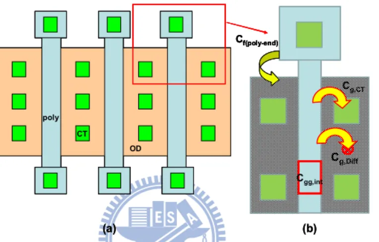
Fig. 3.21 (a) Schematical illustration of multi-finger MOSFET layout (b) three components of
fringing capacitances associated with each gate finger : Cf(poly-end) represents finger-end
fringing capacitance, Cg,Diff, and Cg,CT are gate sidewall fringing capacitances...48
Fig. 3.22 Effective mobility eff versus VGT for narrow-OD NMOS determined with
consideration of W in Weff and Cgg,int for Qint. Narrow-OD NMOS : W1N32, W05N54,
standard : W2N16. Linear operation condition : VDS=0.05V, VGT=VGS - VT...52
Fig. 3.23 Effective mobility eff versus VGT for multi-OD NMOS determined with
consideration of W in Weff and Cgg,int for Qint. Multi-OD NMOS : OD8 (WOD=0.25m),
OD16 (WOD=0.125m), standard : OD1 (WOD=2m)W2N16. Linear operation condition :
VDS=0.05V, VGT=VGS - VT...53
Fig. 3.24 Effective mobility eff versus VGT for donut MOSFET determined with
consideration of W in Weff and Cgg,int for Qint. (a) NMOS (b) PMOS, donut : D1S1, D10S10,
standard : W2N32. Linear operation condition : VDS=0.05V, VGT=VGS - VT...54
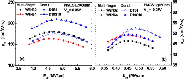
Fig. 3.25 Effective mobility eff versus Eeff for narrow-OD NMOS determined with
consideration of W in Weff and Cgg,int for Qint. Narrow-OD NMOS : W1N32, W05N54,
standard : W2N16. VDS=0.05V, Eeff (VGT 2VT) / 6Tox inv( )...55
Fig. 3.26 Effective mobility eff versus Eeff for multi-OD NMOS determined with
consideration of W in Weff and Cgg,int for Qint. Multi-OD NMOS : OD8 (WOD=0.25m),
OD16(WOD=0.125m), OD1 (WOD=2m). VDS=0.05V, Eeff (VGT 2VT) / 6Tox inv( )...56 Fig. 3.27 Effective mobility eff versus Eeff for donut MOSFET (D1S1, D10S10) determined
with consideration of W in Weff and Cgg,int for Qint (a) NMOS : Eeff (VGT 2VT) / 6Tox inv( ) (b)
PMOSEeff (VGT 3VT) / 9Tox inv( )...56
Fig. 3.28 Effective mobility eff versus Eeff for donut MOSFET (D1S1, D10S10) and a
xiii
( )
( 2 ) / 6
eff GT T ox inv
E V V T (b) PMOSEeff (VGT 3VT) / 9Tox inv( )...57
Fig. 3.29 Effective mobility eff versus Eeff for multi-finger NMOS (W2N16, W1N32, W05N64). Eeff (VGT 2VT) / 6Tox inv( ) . Three regions corresponding to three scattering mechanisms : coulomb scattering in low field, phonon scattering in medium field, and surface roughness scattering in high field...57
Fig.3.30 Schematic of experimental set-up of the charge pumping measurement applied to MOSFET with four terminals...59
Fig.3.31 CP pulse waveform : tr and tf are the rising and falling times, Vbase and Vh are swept from accumulation (Vbase <VFB) to inversion (Vh >VT), under fixed pulse amplitude Va=Vh-Vbase,...60
Chapter 4
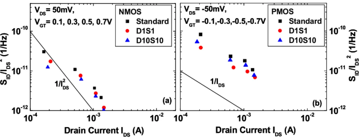
Fig. 4.1 The low frequency noise SID/IDS2 measured for the multi-finger NMOS W2N16, W1N32, and W05N64...62Fig. 4.2 SID/IDS2 vs. IDS under varying |VGT| (0.1~0.7V) for NMOS narrow-OD devices...63
Fig. 4.3 SID/IDS2 vs. IDS under varying VGT (0.1~0.7V) for OD1 and OD16 devices...63
Fig. 4.4 SID/IDS2 vs. IDS under varying |VGT| (0.1~0.7V) for NMOS multi-OD devices...64
Fig. 4.5 The low frequency noise SID/ID2 measured for the multi-OD devices, OD1, OD8, and OD16...65
Fig. 4.6 SID/IDS2 vs. IDS under varying |VGT| (0.1~0.7V) for PMOS multi-OD devices...66
Fig. 4.7 The low frequency noise SID/ID2 measured for the standard and donut devices (a) NMOS (b) PMOS: Standard (multi-finger W2N32), Donut D1S1, and D10S10...67
Fig. 4.8 SID/IDS2 vs. IDS under varying |VGT| (0.1~0.7V) for standard and donut devices (a) NMOS (b) PMOS Standard : multi-finger W2N32, Donut, D1S1 and D10S10...68
xiv
Fig. 4.9 Normalized PSD of drain current noise SID/IDS2 vs. frequency, measured from (a)
W2N32 NMOS and PMOS (b) W1N64 NMOS and PMOS, under |VGT|=0.3V and
|VDS|=0.05V...69
Fig. 4.10 Normalized PSD of drain current noise SID/IDS2 vs. frequency, measured from
multi-OD MOSFET (a) OD8 (WODxNOD=0.25mx8) : NMOS and PMOS (b) OD16
(WODxNOD =0.125mx16) : NMOS and PMOS, under |VGT|=0.3V and |VDS|=0.05V. multi-OD
MOSFET : NF=16, WODxNOD =2 m...69
Fig. 4.11 Comparison of measured charge pumping current with different pulse amplitude
(Va)...71
Fig. 4.12 Charge pumping current measurement of standard and multi OD device...72
Fig. 4.13 Interface trap density Nit of OD1 and OD16 devices extracted by using Weff and W,
measured at VD=VS= VB= 0V and Va = 1.7V...73
Fig. 4.14 Charge pumping current of three narrow OD devices, and maximum charge
pumping current comparison among each measurement die...74
Fig. 4.15 Interface trap density Nit of narrow-OD devices extracted by using Weff and W,
measured at VD=VS= VB= 0V and Va = 1.7V...74
Fig. 4.16 Hooge’s parameter versus gate-over-drive voltage |VGT| for standard and doughnut
devices biased at |VGT|= 0.1~0.7V...75
Chapter 5
Fig. 5.1 General two-port network...76 Fig. 5.2 The extracted Rg of standard and doughnut devices as a function of frequency with
VDS= 1.2V, VGS= 1V...78
Fig. 5.3 Comparison of (a) Z-method and (b) Y-method Rg extraction for NMOS standard and
doughnut devices...79
Fig. 5.4 Comparison of (a) Z method and (b) Y method Rg extraction for PMOS standard
xv
Fig. 5.5 Comparison of (a) Z method and (b) Y method Rg extraction for NMOS narrow-OD
Device...82
Fig. 5.6 Comparison of (a) Z method and (b) Y method Rg extraction for NMOS multi-OD
Device...83
Fig. 5.7 (a) The cut-off frequency fT versus VGT measured for multi-OD devices(b) Cgg versus
VGS extracted from Y-parameters for multi-OD devices...85
Fig. 5.8 (a) Ugain and (b) fMAX extraction for multi-OD NMOS...86
Fig. 5.9 (a) Ugain and (b) fMAX extraction for narrow-OD NMOS...87
Fig. 5.10 The cut-off frequency fT vs. Vgs measured for standard and donut devices (a) NMOS
(b) PMOS. Standard : multi-finger W2N32. Donut : D1S1 and D10S10...87
Fig. 5.11 Cgg vs. Vgs extracted from Y-parameters for standard and donut devices (a) NMOS
(b) PMOS. Standard : multi-finger W2N32. Donut : D1S1 and D10S10...88
Fig. 5.12 Comparison of NFmin measurement result of standard and doughnut devices
of NMOS (left) and PMOS (right)...90
Fig. 5.13 Comparison of Rn measurement result of standard and doughnut devices
of NMOS (left) and PMOS (right)...90
Fig. 5.14 Comparison of Ysopt measurement result of standard and doughnut devices of
NMOS (left) and PMOS (right)...91
Fig. 5.15 Comparison of noise parameters measurement result of standard and narrow-OD
devices, (a) NFmin (b) Rn...92
Fig. 5.16 Comparison of noise parameters Re(Ysopt) and Im(Ysopt) measurement result of
standard and narrow-OD devices...92
Fig. 5.17 Comparison of noise parameters measurement result of standard and multi OD
xvi
Fig. 5.18 Cjs extraction versus frequency (a) without Rbb calibration and (b) after Rbb...97
Fig. 5.19 Cjd extraction versus frequency (a) without Rbb calibration and (b) after Rbb
calibration ...98
Fig. 5.20 Cgs and Cgd extraction versus frequency of ring type body contact layout...99
Fig. 5.21 Cjs extraction versus frequency of ring type body contact layout...99
Fig. 5.22 Cjd (Cbd and Cdb) andCjd (Cbs and Csb) extraction versus body bias (a) standard and
xvii
Table Captions
Chapter2
Table 2.1 (a) RF and Analog Mixed-Signal CMOS Technology Requirements – Near term [4]...6 Table 2.1 (b) RF and Analog Mixed-Signal CMOS Technology Requirements – Long term [4]...7 Table 2.2 Load resistors and filter resistors used in 9812B pre-amplifier...18
Chapter3
Table 3.1 Stress favorable for mobility enhancement in NMOS and PMOS along longitudinal
and transverse directions [29]...24
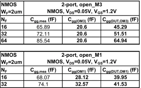
Table 3.2 Gate capacitances measured from multi-finger MOSFET (Cgg,mea), dummy open
structures (Cgg(OM3), Cgg(OM1)), Cgg(DUT,OM3) and Cgg(DUT,OM1) after openM3 or openM1
deembedding...43
Table 3.3 Cgg(DUT,OM3) and Cgg(DUT,OM1), extracted from openM3 and openM1 deembedding on
multi-finger NMOS with NF=16, 32. Cgg(M3) and Cgg(M1~M3) calculated by Raphael simulation
for dummy openM3 and dummy openM1. A comparison of Cgg(M1~M3)=Cgg(DUT,OM3)-
Cgg(DUT,OM1) from measurement and Cgg(M1~M3)=Cgg(M1~M3)-Cgg(M3) from simulation...43
Table 3.4 Multi-finger MOSFET device parameters extracted from DC I-V and RF C-V
characterization flow...51
Chapter5
Table. 5.1 The optimized parameters (Ag and B) for Z method Rg extraction of standard
W2N32 device...80
Table. 5.2 The optimized parameters (Ag and B) for Z method Rg extraction of doughnut
D1S1 device...80
Table. 5.3 The optimized parameters (Ag and B) for Z method Rg extraction of doughnut
D10S10 device...81
Table. 5.4 The layout view and classification of each kind body contacts...95 Table. 5.5 Cjs extraction versus Vgb extraction...98
xviii
Table. 5.6 The increment of Cjs with the body ring number increased...98
Table. 5.7 Body resistance and deep-N-well capacitance with different body
1
Chapter 1
Introduction
1.1 Research Motivation
Recent advances in the CMOS technology, which possesses the advantage of high
integration and low power, is finding more and more important applications in the area of
analog, mixed mode, and RF circuits [1,2]. RF integrated circuit design requires accurate
device models up to the operating frequency, especially when the operating frequency of the
circuit approaches the cutoff frequency (fT) or maximum oscillation frequency (fMAX).
As devices scaled down into the nanometer-scale regime, the stress induced from shallow
trench isolation (STI) process and its impact on the device performance becomes significant
[3]. The longitudinal stress effect has been widely investigated; however, relatively fewer
studies were focused on the transverse stress effects. Besides, STI stresses, either longitudinal
or transverse, exhibits high sensitivity to device layouts, which may significantly impact the
analog circuit performance. Meanwhile, the increase of effective, namely W from STI top
corner rounding (TCR) emerges as an important factor besides STI stress to affect DC
characteristics (drain current and trans-conductance), low frequency noise, and high
frequency performance.
The multi-finger transistors have been widely as the standard layout in RF circuits to
enhance fMAX and reduce RF noise by minimizing the parasitic gate resistance. In this thesis,
three kinds of layouts, namely doughnut (donut), narrow-OD, and multi-OD MOSFETs have
been designed to investigate layout dependence of STI stress, particularly the transverse stress.
A comprehensive characterization was carried out to investigate the transverse stress effect on
mobility, current, low frequency noise (LFN), and high frequency performance. Mullti-finger
2
Four-port test structures adopting five kinds of body contact layouts, denoted as multi-ring,
U-shape, L-shape, parallel, and perpendicular stripe have been designed to explore the
influence on basic device parameters like body resistance and junction capacitances, and the
proliferated impact on low frequency noise and high frequency performance.
1.2 Thesis Organization
This thesis presents our research results of RF MOSFET layout effect on low frequency
noise and high frequency characteristics, with major purpose for RF and analog circuit
applications. The main effect of our focus is the mechanical stress introduced from shallow
trench isolation (STI), which increases with technology scaling and becomes dramatically
significant in nanometer scale devices. In this thesis, three types of new MOSFET layout,
namely narrow-OD, multi-OD, and donut devices are proposed to modulate the transverse
stress from STI.
At first, an overview on low frequency noise theory and measurement methods is presented
in chapter 2. Then, the layout dependence of STI stress and its effect on device parameters
like drain current (IDS), transcondutance (Gm), and effective mobility (eff) are described in
chapter 3. The proposed new MOSFETs with layouts of narrow-OD, multi-OD, and donut
were fabricated in 90 nm low leakage CMOS process. An extensive device characterization
has been carried out through I-V, C-V, S-parameters, and charge pumping (CP) current
measurements. Note that the C-V characterization was performed based on S-parameters
measurement, which can solve the problems of conventional C-V measurement, such as the
parasitic capacitances from pads, interconnection lines, and substrate coupling and gate
leakage induced abnormal C-V fall-off. However, one more parasitic capacitance arising from
3-D gate fringing effect cannot be removed from the open deembedding method implemented
in S-parameters characterization. Thus, 3-D RLC simulator like Raphael was employed in this
3
Based on the mentioned characterization techniques, STI top corner rounding (TCR) is
identified as a key factor affecting I-V, Gm, gate capacitances, LFN, and high frequency
performance, etc.
In chapter 4, MOSFET layouts effect on LFN will be presented, with a
comprehensive characterization on all of the device structures such as standard multi-finger,
narrow-OD, multi-OD, and donut MOSFETs, and covering both NMOS and PMOS. The
layout effect can be examined through an extensive comparison between different device
structures. Also, the interface trap density Nit extracted by CP method is taken as one of key
parameters responsible for flicker noise, i.e. LFN under the condition that number fluctuation
model is the dominant mechanism, tentatively for NMOS. Two more topics to be covered in
chapter 4 are the body contact layouts effect and strain effect on LFN. In this study, totally
five body contact layouts, such as multi-ring, U-shape, L-shape, parallel and perpendicular
stripes are designed for an investigation on their effect on LFN. A review of strain effect will
be classified as stress from strain engineering in 65nm high speed CMOS process and STI
stress from new MOSFET layouts introduced in chapter 3. Chapter 5 will focus on MOSFET
layout effect on high frequency characteristics, such as fT, fMAX, and RF noise parameters. An
extensive characterization will cover different device structures and also the dependence of
frequency and bias. Note that two-port or four-port deembedding is indispensable in high
frequency characterization for parasitic RLC extraction and elimination, which is necessary
for an accurate extraction of intrinsic device performance under high frequency operation. As
for body contact layout effect, four-port test structure is required to accommodate 4-terminal
MOSFETs with separate body terminal and a new body network model has been developed to
simulate the body contact layout and body biases effects. In the end, chapter 6 concludes this
4
Chapter 2
Low Frequency Noise Theory and Measurement Method
2.1 An Overview of CMOS Technology and Low Frequency Noise
It has been well known that noise exists as a fundamental problem in semiconductor
devices and electronic circuits. In electronic devices, noise appears as random fluctuations in
current or voltage around their DC level, due to fluctuations in carriers transport through the
conduction channel. The impact from noise on the desired signal may cause failure of
electronic circuits operation when the noise power becomes too large to keep sufficient signal
to noise ratio (SNR). Furthermore, the mentioned problem becomes increasingly tough in
miniaturized devices accompanied with supply voltage scaling and squeezed dynamic range.
Attributed to the nature of random fluctuations, noise is generally characterized by probability
density function (PDF) based on multiple measurements over time. The time average of the
measured noise currents or noise voltages approaches zero when integrated long enough and
provides no useful information; instead, the square quantities namely power spectral density
(PSD) is used to characterize noise. The PSD is measured with a spectrum analyzer or
dynamic signal analyzer, which will be described in section 2.2.
The experimental indicates that the noise spectral density increases with decreasing
frequency at lower frequencies and becomes white thereafter. The corner frequency between
the frequency dependent noise and white noise is typically from few Hz up to MHz range and
may vary with device types, device dimensions, and bias conditions, etc. The physical
mechanism behind the white noise source is well known. However, the excess noise at low
frequencies, namely low frequency noise (LFN) brings many questions with lot of debates
and open up an interesting research area. Note that the LFN is also known as flicker noise or
5
The aggressive advancement of CMOS technology into nanoscale regime in recent five
years has driven transistor gate delay to below 10 ps and intrinsic cut-off frequency (fT) well
above 100 GHz [4]. According to International Technology Roadmap for Semiconductor
(ITRS) [4], the demand on devices and interconnection lines scaling in the area of analog and
RF is not as stringent as that for high speed logic CMOS. However, much more stringent
criterion on the flicker noise at low frequencies (i.e., LFN) and thermal noise at high
frequencies is required and specified for analog and RF circuit design, as shown in Table 2.1(a)
and (b) for near term and long term, respectively [4]. The yellow blocks marked for
2011~2014 represent that the manufacturing solutions are known but not yet optimized.
Unfortunately, the red blocks marked for 2015 and thereafter highlight the problems for which
the manufacturable solutions do not exist today. Obviously, the 1/f noise, i.e. LFN emerges as
a big roadblock from 2015 and on. As compared with bipolar transistors, CMOS transistors
generally suffer higher flicker noise (LFN), due to the nature of surface channel conduction.
As a result, the solutions to suppressing LFN become more challenging to CMOS technology,
even though CMOS is superior in terms of scalability, high integration, low cost, and low
standby power. To facilitate the extension of CMOS technology into RF and analog domain,
an in-depth study on LFN in MOSFETs and its dependence on layouts and geometry scaling
becomes critically important and is selected as one of research topics in this thesis. It has been
recognized that LFN in transistors introduces particular problem in analog and RF circuits
like voltage controlled oscillators (VCOs) and mixers. For VCOs, the LFN is upconverted to
phase noise at small frequency offsets from the carrier frequency and then sets the ultimate
separation limitation to two channels [5-8]. Fig. 2.1 illustrates schematically phase noise
spectrum and different physical origins. As for mixers, the LFN originated from transistors
may lead to severe degradation of SNR [9,10]. This can be understood if the signal is
6
overwhelm the signal, particularly worse for low voltage operation. The impact from LFN on
mixer may be relieved by using long channel transistors; however the penalty of to be paid is
the degradation of transconductance and circuit speed.
7
Table 2.1(b) RF and Analog Mixed-Signal CMOS Technology Requirements – Long term [4]
8
2.2 Low Frequency Noise Theory
In the past several decades, the origins and physical mechanisms underlying flicker
noise remain an open question, with lot of debates and arguments in the experimental results
and modeling to match the measurement. Number fluctuation model and mobility fluctuation
model appear as two most popular mechanisms to explain and predict the measured flicker
noise [11,12]. In 1957, McWhorter published a flicker noise model based on quantum
mechanical tunneling transitions of electrons between the gate oxide and channel [11]. In
practice, the tunneling time varies exponentially with distance, and it is assumed that trap
density is uniform in both energy and distance from the channel interface to extract the time
constants for generating flicker noise. The McWhorter model, namely number fluctuation
model may be useful due to its simplicity and good agreement with experimental, particularly
for n-channel MOSFETs [12,13]. However, the mobility fluctuation model appears to better
explain the flicker noise measured from p-channel MOSFETs [14,15]. As compared to surface
channel MOSFETs, buried-channel MOSFETs or bipolar junction transistors (BJT)
demonstrate significantly lower flicker noise [16-21]. The published results are in favor of the
number fluctuation model that the flicker noise is originated from the traps in the oxide or at
oxide/channel interface. However, the surface carrier mobility is reduced compared to the
bulk value due to additional surface scattering (acoustic phonon and surface roughness),
which has an impact on the mobility fluctuation. Hooge mobility noise [22], which is
sensitive to the crystalline quality, can be employed to explain the higher flicker noise for
surface channel devices in which the carriers are in close proximity to the gate oxide and may
suffer aggravated mobility fluctuation. In the following, the number fluctuation and mobility
9
2.2.1 Number Fluctuation Theory [11]
The physical mechanism underlying the number fluctuation noise is the interaction
between the channel carriers and slow traps in the gate oxide, which is illustrated in Fig. 2.2.
The dynamic exchange of carriers between the gate oxide and channel causes a fluctuation in
the surface potential (S) and then gives rise to fluctuations in the inversion carrier density
Qinv. This in turn leads to noise in the drain current. Note that Qinv (the fluctuation in the
inversion carrier density) can occur even without a current flowing the channel and the
channel current is only used to sense the fluctuations. The mathematical formulas for
expressing number fluctuation model in different operation regions are provided as follows
In weak inversion region
2 2 2 2 , 1 DS I t D it DS ox B ox S N q C C f m I WLC k T m C (2.1)
In strong inversion region
2 2 1 : m m ox eff DS DS GS T g W linear region g C V L I V V (2.2) 2 2 2 2 2 2 2 3 2 1 DS I B t m B t ox eff DS DS ox DS DS S q k T N g q k T N WC V I f WLC I f L I (2.3) 2 2 1 saturation : m m ox sat DS GS T g region g WC I V V (2.4) 2 2 2 2 2 1 1 DS FB I B t V DS GS T ox GS T S q k T N S I V V f WLC V V (2.5) : -t
N the density of traps at quasi Fermi level
The frequency dependence with the exponent may deviate from 1 under the condition that
the trap density Nt is not uniform in depth. For the case when the trap density near the gate
10
smaller than 1. For the opposite case, may become larger than 1. As for the bias dependence
predict by the number fluctuation model, the normalized drain current noise SIDS/IDS2 varies
with approximately as 1/IDS2 or 1/(VGS-VT)2 in strong inversion region given by (2.2)~(2.5)
while is nearly independent of bias in weak inversion region, shown in (2.1). In this work, the
LFN in terms of SIDS/IDS2 measured from n-channel MOSFETs just follows number
fluctuation model and varied with IDS according to the relationship of 1/IDS2.
Fig.2.2 Schematical illustration of electrons in the channel of MOSFET moving in and out of the traps giving rising to fluctuations in the inversion carrier density and thereby the drain current.
2.2.2 Mobility Fluctuation Theory
Mobility fluctuation is another mechanism, which can contribute flicker noise. The
mobility fluctuation model was first proposed by F.N. Hooge with an empirical formula given
for the resistance fluctuation [23]. According to the Hooge empirical formula, the drain
current noise generated by fluctuation in the channel carrier mobility can be written as (2.6).
2 DS I H DS inv S q I fWLQ (2.6)
where H is a dimensionless parameter and referred as Hooge parameter. The typical values of
H range between 10-3 and 10-6 for surface channel transistors. H may be down to 10-7 for
buried channel transistors like N+ gate pMOSFETs and even lower to the order of 10-8 for
11
fluctuation noise [22]. The effective mobility eff of the channel carriers is determined by
different scattering mechanisms, which vary in different ways with the effective normal field
E⊥eff as a function of inversion carriers density QINV and body depletion charge QB. As a result,
H is not only dependent on technology but also on the bias conditions. In general, each
scattering process generates mobility fluctuation noise with the amount given by each
respective Hooge parameter, denoted as Hj. Assume the scattering processes are independent
of each other and then Matthiessen’s rule can be applied as follows
1 1
j
eff j
(2.7)The fluctuations in different scattering processes are assumed independent. Then the variation
applied to (2.7) can lead to
2 2 j eff j eff j
(2.8)The power spectral density can be derived as
2 2 2 j DS I eff j DS j j S S I
(2.9) , 2 j H j j inv S q fWLQ (2.10) 2 2 , Hj eff eff H H H j j j inv j inv j q q fWLQ fWLQ
(2.11) It can be understood from (2.11) that H varies with biases due to the bias dependent factor
eff /j
2. The total drain current noise is evaluated by adding the noise contribution from each channel segment derived for linear region as follows.2 2 0 2 DS DS V I H eff H eff DS DS DS DS S q W q dV V I fWL I fL I
(2.12)12 2 1 1 ( ) DS I H H DS ox GS T ox GT S q q I f WLC V V f WLC V (2.13)
The drain current noise contributed from mobility fluctuation as shown in (2.13) predicts that
the larger H and shorter channel length (L) will lead to higher flicker noise whereas the
wider channel width (W) and higher gate overdrive VGT can help reduce the flicker noise. The
thinner gate oxide thickness is another beneficial factor, which can suppress flicker noise. In
our experimental, the mobility fluctuation model can provide much better fit to the flicker
noise measured from p-channel MOSFETs than number fluctuation model.
2.3 Low Frequency Noise Measurement System
Three flicker noise measurement systems with different equipment configurations are
employed in this thesis for characterization of low frequency noise (LFN) in MOSFETs with
different layouts. The conventional one is Celestry 9812B Noisepro system, which is
supported by NDL and has been commonly used in transistor flicker noise characterization
but limited to measurement using DC probes. The other two are new systems built up in our
RF Lab. – one is SR570 system and the other one is model-5184 system. The major difference
from Celestry 9812B is that these two LFN systems can support both RF and DC test
structures, with RF GSG probes and DC probes, respectively. SR570 system shown in Fig.
2.3 is equipped with SR570 LNA (trans-resistances amplifier), Agilent DSA 35670 (dynamic
signal analyzer), and HP4142B (DC power supply). The model-5184 LNA shown in Fig. 2.4
contains 5184 LNA (voltage amplifier), PA14A1 for ultra low noise DC source, low pass filter,
Agilent 35670, and HP4142B. Note that Agilent ICCAP is adopted for measurement
auto-control and data collection.
1) SR570 Low Frequency Noise Measurement System
13
trans-resistances amplifier produced by Stanford Research Systems. Essentially, LNA acts as
a key element in this flicker noise measurement system through which it can provide the
second stage low noise gain to reduce system noise and offer sufficiently large signal
amplitude to dynamic signal analyzer (DSA) without increasing the undesired noises. In
practice, the SR570 LNA can provide an offset current source at the DUT output (i.e., drain
terminal of MOSFETs), which serves as an input to the amplifier. The DUT output current can
be modulated by the low noise offset current source, so as not to drive the amplifier into
saturation. The SR570 is also equipped with a filter with different options, such as low-pass,
high –pass or bandpass filter. In our applications, we typically set bandpass filter to select the
frequency range of our interest, i.e. 1 ~ 100k Hz. The HP4142B DC power supply was
controlled by ICCAP to provide the gate bias for MOSFET through a low pass filter in order
to remove the power supply’s noise within the frequency range of interest that is above 1Hz.
In other words, the supply voltage through the low pass filter is nearly a pure DC voltage
source under the condition that the signal above 1Hz was removed by the low pass filter. The
LNA output is connected to DSA, which can perform dynamic signal (V/ Hz) measurement
and analysis. All the equipments such as 4142B, SR570 LNA, and Agilent DSA 35670 are
integrated together and the measurement can be carried out through the control of ICCAP .
Through a dynamic signal analysis done by DSA, we can obtain the measured noise from
ICCAP. In general, we have to make a simple calculation to recover the original noise
measured from DUT output stage. The measured noise is transformed to current spectrum
14
Fig.2.3 Schematic of SR570 flicker noise measurement system setup with SR570 LNA
(trans-resistance amplifier), Agilent DSA 35670 (dynamic signal analyzer), and HP4142B (DC power supply)
Unfortunately, The measurement system adopting SR570 LNA has a stringent current
limitation of 5 mA. For advanced multi-finger RF MOSFETs, which sometimes have large
total width for sufficient current drivability and transconductance, this current limitation
generally restricts the DUTs to limited operation conditions, such as linear or subthreshold
regions. To solve the mentioned problem, we proposed a new system configuration by using
model-5184 LNA to overcome the current limitation. Unlike SR570, model 5184 LNA is a
kind of voltage amplifier with a separated output bias source. In the following, we will have a
discussion on this new LFN measurement system.
2) New Configuration with Model 5184 LNA and ultra low noise DC source (PA14A1)
An appropriate operation of SR570 LNA requires that the gain setting resistor should be
lower than the output resistance of DUT (rout). As for the new solution using model 5184 LNA
(voltage amplifier), the voltage gain and LNA noise are independent of the output resistance
of DUT. In this way, the LNA noise is independent of the DUT and thus we can obtain a
system noise level from measurement without DUT. The noise floor of the system can be
pushed to 10-20 (V2/Hz), which is well below that of DUT in the frequency range of our
15
DUT output biasing source, thus reducing the system integration level. Therefore, a reliable
and ultra-low noise DC source at DUT output is required to minimize the extra noise
contributed from the system. Battery is one of low noise sources, which can effectively reduce
the noise generated from power supply. Besides the simple setup using batteries, we propose a
new solution using an ultra low noise DC source (PA14A1) instead of batteries. A complete
system configuration incorporating batteries or low noise DC source (PA14A1) is illustrated
in Fig. 2.4. In practice, we implement on a PCB (printed circuit board) the metal lines in three
paths for connecting LNA (model 5184), low noise source (PA14A1), and DUT drain terminal
as shown in Fig. 2.5 (a) and (b).
In Fig.2.5(b), the ultra low noise DC source (PA14A1) was used. The advantage of using
PA14A1 is that it can achieve the desired output voltage but a simple setup with batteries
shown in Fig. 2.5(a) cannot meet the requirement.
In conclusion, we can obtain almost the same measurement results under the same bias
condition by using SR570 LNA and model 5184 LNA either with batteries or PA14A1.
Besides the mentioned achievement, we have extended this work to 4-terminal MOSFET
16
Fig.2.4 Schematic of low frequency noise measurement system consisting of model 5184
LNA (voltage amplifier), HP4142B for DC supply, and Agilent 35670 for dynamic signal analyzer
(a)
PA14A1 Low noise DC soruce
CH1
(b)
Fig.2.5 New solution for using model 5184 LNA (a) Battery (b) ultra low noise DC source
17 3) Celestry 9812B NoisePro System
Fig. 2.6 illustrate the configuration of Celestry 9812B system, later named as ProPLUS
NoisePro system, which consists of 9812B analyzer (hardware), NoisePro software with
automatic control, and built-in 1/f noise SPICE model parameter extraction routine to
provides off-the-shelf 1/f noise system.
Fig.2.6 Schematic illustration of Celestry 9812B Noisepro system consisting of HP4145 for
DC supply, 9812B for pre-amplifier, and Agilent 35670 for dynamic signal analyzer.
Celestry 9812B system can support noise characterization and model parameter extraction
for MOSFETs, BJTs, diodes and resistors, based on either public or proprietary models. This
system offers V-mode and I-mode biasing modes with accuracy specification of user options.
Detachable pre-amplifier unit can be placed closer to DUTs or in the measurement chamber,
which greatly reduces the system noise floor. The battery operated current amplifier provides
as low as 0.5pA/(Hz)1/2 @ 1 KHz floor noise and voltage amplifier provides 1nV/(Hz) 1/2 @ 1
KHz floor noise.
When proceeding a system calibration, NoisePro will automatically perform a leakage
testing, and the system will apply voltage of 1-Volt and measure the leakage current. The
measured values of leakage and load resistors will be saved in a file to be used in the noise
18
and version of noise amplifier, their values differ. Table 2.2 lists the default values of load
resistors (Rload) used in noise amplifiers and those of filter resistors in load circuit. If 9812B is
selected, user needs to choose the type of amplifier : current or voltage amplifier, internal or
external amplifier. If external amplifier is selected, the user needs to provide method of
converting the A, B, C values.
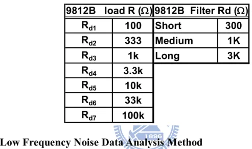
Table 2.2 Load resistors and filter resistors used in 9812B pre-amplifier
Rd1 100 Short 300 Rd2 333 Medium 1K Rd3 1k Long 3K Rd4 3.3k Rd5 10k Rd6 33k Rd7 100k 9812B load R () 9812B Filter Rd ()
2.4 Low Frequency Noise Data Analysis Method
As mentioned previously, an extensive noise characterization indicates that low frequency
noise (LFN) in nMOSFETs follows the number fluctuation model whereas that in pMOSFET
is in better agreement with mobility fluctuation model. For MOSFETs, the measured LFN is
generally expressed as normalized PSD (power spectral density) of drain current noise,
denoted as SID/IDS2 to identify which model is the dominant one in the devices under test.
According to the normalized PSD derived for number fluctuation model for subthreshold,
linear, and saturation regions in (2.1), (2.3), and (2.5), respectively, the SID/IDS2 is proportional
to 1/IDS2 and increases linearly with oxide trap density Nt. On the other hand for the
normalized PSD governed by mobility fluctuation model, expressed in (2.12) and (2.13) as a
function of IDS and VGT, respectively, the SID/IDS2 is proportional to 1/IDS or 1/ VGT and
19
overdrive VGT can suppress LFN. Sometimes, the experimental present VGS dependence
stronger than what predicted by model. McWhorter’s carrier trapping model may provide one
of mechanisms responsible for the stronger VGS dependence. The oxide trap density Nt is
known to be a function of the potential energy across the band gap of semiconductor substrate.
When VGS is varied, Fermi level of the channel moves accordingly. If the number of particular
traps that cause flicker noise drastically changes along with the VGS, the noise amplitude
could be a stronger function of the bias. Another factor that we should take into account is the
fact that carrier mobility is also a function of VGT. Regarding device scaling effect, both
models reveal dependence of device dimensions in terms of 1/WLCox2, which means the
channel length and width scaling will lead to increase of SID/IDS2 but the oxide thickness TOX
scaling can help reduce LFN in terms of SID/IDS2. Note that W, L, Cox, eff, H, and VGT appear
as key parameters in LFN models and how to accurately extract or determine the mentioned
parameters becomes critical for LFN data analysis and diagnosis. In LFN models, W and L
represent effective channel width and effective channel length, rather than drawn dimensions
on layout or physical dimensions from optical measurement. The accurate extraction of
effective channel dimensions brings additional challenges for miniaturized MOSFETs with
short channel and narrow width to sub-100 nm regimes in 90nm technology and below. STI
top corner rounding (TCR) effect on effective channel width will be described in chapter 3. As
for Cox, it represents the gate capacitance density per unit area, under strong inversion
condition in which Cox is contributed from three major capacitances in series – gate oxide
capacitance, gate depletion capacitance, and inversion channel capacitance. Again, an
accurate extraction of Cox becomes difficult in miniaturized MOSFETs, due to several
complicated factors like deviations in effective channel length and width, gate depletion effect,
inversion channel quantization effect, and more importantly the parasitic capacitances from
20
enough to minimize or even eliminate the deviation of effective channel dimensions is
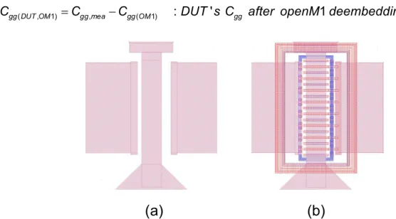
adopted to solve this problem. Furthermore, a dedicated open deembedding to the bottom
metal, i.e. M1 is necessary to approach an accurate extraction of Cox.
The accuracy or deviation of mentioned basic device parameters will have direct impact
on the determination of eff and H. Furthermore, both eff and H are a function of scattering
mechanisms and biases. The bias dependence ofeff and H comes from electrical field effect
on carriers transport and their scattering through the conduction channel. Note that the gate
bias dependence manifests normal field effect and is expressed in terms of gate overdrive
VGT=VGS -VT in which VT variations from processes, geometries, profiles, and biases can be
taken into account. As shown in Fig. 2.7, the measured LFN in terms of SID/IDS2 decrease with
increasing |VGT| for both NMOS and PMOS. Fig. 2.8 (a) and (b) illustrate SID/IDS2 versus VGT
for NMOS and PMOS, respectively and reveal the difference of VGT dependence between
NMOS and PMOS. The results can be explained by (2.3) and (2.5) for NMOS governed by
number fluctuation, and (2.13) for PMOS dominated by mobility fluctuation.
Frequency dependence is one more key factor for LFN analysis and modeling. Assuming
an ideal condition that trap density Nt is a constant, the frequency dependence of flicker noise
will follow 1/f. However, in most of real cases, the exponent in frequency dependence may
deviate from 1 due to the fact that the trap density Nt is not uniform in depth. For the case
when the trap density near the gate oxide/channel interface is higher than that in the interior of
the gate oxide, tends to be smaller than 1. For the opposite case, may become larger than 1.
Referring to Fig. 2.7, the frequency dependence of PMOS (Fig.2.7(b)) follows 1/f very
consistently but that of NMOS (Fig. 2.7(a)) reveals certain deviation from 1/f , with the
exponent < 1.
It has been a conventional belief from analog circuit design using N+ poly gate technology
21
buried channel PMOS, attributed to deeper channel and less surface scattering. However, the
advancement of CMOS process has driven phase-out of N+ poly gate technology and
deployment of dual gate technology, i.e. N+ /P+ poly gate for N/P MOSFET, since 0.25m
technology node and beyond. The dual gate technology can realize surface channel for both
NMOS and PMOS and help push VT scaling for low voltage operation. In this way, the
advantage of PMOS over NMOS, in terms of flicker noise can no longer be maintained. Fig.
2.9 makes a comparison of measured LFN (SID/IDS2) between NMOS and PMOS under the
same bias, i.e. |VGT|=0.3V and |VDS|=0.05V. As can be seen clearly that SID/IDS2 of PMOS is
higher than NMOS by around one order at very low frequency (<10 Hz) and the difference
decreases at higher frequency. The results suggest that conventional design using PMOS in
VCO for low phase noise is no longer valid. A detailed analysis of LFN to investigate the
mechanisms responsible for NMOS and PMOS and the optimization design for suppressing
LFN become an important task.
101 102 103 10-12 10-11 10-10 10-9 (a) VGT=0.2V VGT=0.3V SID /IDS 2 ( 1 /H z ) Frequency (Hz) UMC90nm-97C W2N32 NMOS Vds=0.05V VGT=0.1V 101 102 103 10 -12 10-11 10-10 10-9 (b) SID /IDS 2 ( 1 /H z ) Frequency (Hz) VGT=-0.5V VGT=-0.3V VGT=-0.1V UMC90nmW2N32 PMOS Vds= -0.05V
Fig.2.7 Normalized PSD of drain current noise SID/IDS2 measured from (a) NMOS and (b)
PMOS with increasing frequency, under various VGT (|VGT |=0.1, 0.3, and 0.5V).
22 0.1 1 10-11 10-10 (a) VGT (V) SID /ID S 2 ( 1 /H z ) 90nm NMOS W2N32 W1N64 0.1 1 10-11 10-10 10-9 S ID /I D S 2 ( 1 /H z ) (b) |VGT| (V) 90nm PMOS W2N32 W1N64
Fig.2.8 Normalized PSD of drain current noise SID/IDS2 measured from (a) NMOS and (b)
PMOS under increasing |VGT| and fixed |VDS|=0.05V.
101 102 103 10-12 10-11 10-10 10-9 S ID /I D S 2 ( 1 /H z ) PMOS NMOS Frequency (Hz) 90nm W2N32 |V DS|=0.05V, |VGT|=0.3V
Fig.2.9 Normalized PSD of drain current noise SID/IDS2 versus frequency, measured from (a)
NMOS and (b) PMOS under |VGT|=0.3V and |VDS|=0.05V. NMOS and PMOS were fabricated
23
Chapter 3
Analysis of Layout Effect on STI Stress and Device Parameters
3.1 STI stress Mechanics in RF MOSFET
Shallow trench isolation (STI) emerged to replace LOCOS as the standard isolation
technology in CMOS process at 0.25 m node and below [24,25]. The technology transition
proves itself the success that STI enables continuous scaling of active and isolation regions to
far beyond 0.25m node, and realize higher integration level for IC design. Also, STI brings
the advantages like reduced sidewall capacitance for AC performance and improved surface
planarity for high integration [26]. In spite of the mentioned advantages, STI indeed
introduces some other impacts, such as mechanical stress from refilled trench or known as
Length of Oxide Definition (LOD) stress-effect [27,28]. The STI stress may have a significant
influence on MOSFETs’ electrical characteristics, such as threshold voltage (VT), carrier
effective mobility (eff), transconductance (Gm), gate speed, cut-off frequency (fT), and low
frequency noise, etc. The mentioned impacts always increase with devices scaling and
becomes the key factors of consideration in MOSFETs layout for integrated circuit design,
particularly for RF and analog circuits of our focus in this thesis.
The STI module implemented in standard CMOS processes from 0.25m to 65nm
nodes generally introduce compressive stress, either along or transverse to the channel
length, i.e. the current flow direction. The stress along the channel length is defined as
longitudinal stress //, and that transverse to the channel length is denoted as transverse
stress⊥. The reverse type of stress, namely tensile stress will introduce its influence in the
opposite direction with that of compressive stress. The impact from STI stress on device
characteristics is strongly dependent on the device types and orientations. Table 3.1
summarizes the stress favorable for mobility enhancement and reveals fundamental