行政院國家科學委員會專題研究計畫 成果報告
具有低介電常數阻障介電薄膜製程整合之研究(2/2)
計畫類別: 個別型計畫 計畫編號: NSC92-2215-E-009-019- 執行期間: 92 年 08 月 01 日至 93 年 07 月 31 日 執行單位: 國立交通大學電子工程學系 計畫主持人: 施敏 共同主持人: 張鼎張 報告類型: 完整報告 報告附件: 出席國際會議研究心得報告及發表論文 處理方式: 本計畫可公開查詢中 華 民 國 93 年 11 月 22 日
行政院國家科學委員會專題研究計畫期末報告
具有低介電常數阻障介電薄膜製程整合之研究(2/2)
Study on the integration of barrier dielectric with low
dielectric constant
計畫編號:NSC 92-2215-E-009-041
執行期間:92 年 8 月 1 日至 93 年 7 月 31 日
計畫主持人:施 敏
共同主持人:張鼎張
計畫參與人員:蔡宗鳴、陳紀文、張大山、陳世璋
一.中文摘要 研究積體電路製造技術中的多層導體 連線製程。隨著半導體技術的進步,元件的 尺寸也不斷地縮小,而多層金屬導體連線的 設計,也成為超大型積體電路技術所必須採 用的方式。然而,隨著金屬導線層的數目增 加及導線間的距離不斷縮小,電子訊號在金 屬連線間傳送時,金屬連線的電阻-電容延 遲時間(RC delay time),變成半導體元件 速度受限的主要原因。為了降低訊號傳遞的 時間延遲,現今已經發展以金屬銅(電阻率 為 1.7μΩ-cm)來取代金屬鋁(電阻率為 2.7μΩ-cm)成為導線的連線系統。而在降 低電容方面,則朝向低介電常數 ( low-k ) 材料發展。但是在銅與鑲嵌的製程與電性操 作的環境下,溫度與電場的作用,銅極易擴 散至低介電常數材料中,並與之發生反應, 造成材料特性的劣化與漏電流增大,甚至導 致介電質崩潰。因此,在符合製程相容性要 求的前提之下,發展具抗銅金屬擴散特性的 介電阻障層材料,便成為重要的研究課題。 目前一種含氧碳化矽(silicon carbide)材料薄 膜,具有低的介電係數(k~3.7),因此受到廣 大的矚目,而被應用於介電阻障層技術中, 用 來 取 代 傳 統 具 高 介 電 係 數 的 氮 化 矽 (silicon nitride) (k~8),以降低導線系統的延 遲時間。本研究將討論含氧碳化矽膜的基本 物性及電性,以及其在製程整合時遇到氧電 漿處理以及後段製程受溫度的影響其薄膜 對抗銅能力的探討。最後,將樣品放置在低 溫的環境下,探討其漏電機制 關鍵詞:低介電數材料, 含氧碳化矽 Abstract
We know that the metal linewidth and spacing decreases with the device scaling, resulting in large RC time delay. Copper is an applicable alternative due to its low resistivity (1.7 µΩ-cm), which is much lower than that of Al (2.7 µΩ-cm). Besides, copper is more resistant to electromigration problem, which is a vital issue in device reliability. The diffusion barrier layer is also served as the etch stop layer during trench formation if necessary. Silicon nitride (SiN) is the currently standard barrier layer material since it has been employed as a masking and passivating layer for a long time against diffusion of metal ions and moisture. Unfortunately, the relative high
dielectric constant (~7) of SiN conflicts with the requirement of low dielectric IMD. Therefore, it is urgently desirable to seek a new barrier layer material. Recently, a newly-developed dielectric barrier material, amorphous SiOC:H has aroused much attention.
In this thesis, we study the fundamental concepts and the intrinsic properties and the effect of O2 plasma ashing and temperature in BEOL process on the barrier properties of the SiOC:H film against copper penetration. Finally, we let the sample at low temperature and measure its electrical characteristics Key word: low-k, SiOC:H
二.緣由與目的
Cu has been recognized as the most appropriate alternative for Al as wiring material due to its low electrical resistivity and excellent electromigration resistance [1], [2]. Dual damascene process is the well-accepted patterning technology since it is difficult to pattern Cu film by plasma etching. However, some challenges exist while Cu is to be integrated into the process. It is known that Cu is a serious contamination source for both silicon and silicon dioxide. To prevent Cu from diffusion into IMD, Cu must be sealed by diffusion barriers. The main IMD is essentially some kind of low dielectric constant (low-k) materials. Moreover, a dielectric diffusion barrier layer depositing on Cu wires is necessary to seal Cu and served as the etch stop layer during the via etching of the subsequent layer. This diffusion barrier layer is also served as the etch stop layer during trench formation if necessary. Silicon nitride (SiN) is the currently standard barrier layer material since it has been employed as a masking and passivating layer for a long time against diffusion of metal ions and moisture [3], [4], [5]. Unfortunately, the relative high dielectric constant (~7) of SiN conflicts with
the requirement of low dielectric IMD [6]. The impact of SiN on interconnection capacitance becomes more prominent with the decrease of dielectric constant of main IMD. Therefore, it is urgently desirable to seek a new barrier layer material. Recently, a newly-developed dielectric barrier material, amorphous SiOC:H has aroused much attention. It has been widespreadly regarded as the only candidate to replace SiN as the dielectric diffusion barrier and the etch stop layer [7],[8].
In this thesis, we will investigate the intrinsic electric properties of the SiOC:H film and its reliability against Cu contamination.
三.結果與討論
The various concentrations of oxygen were controlled by O2 gas flow rate during PECVD process. The silicon carbide film was deposited on 8 inch p-type doping silicon wafer with a resistivity of 15-25 Ω-cm. The code name of the pure silicon carbide film in this study is “SiOC”; besides, the code names of silicon carbide films with various flow rate of O2 gas during PECVD process are “SiOC1”, “SiOC2” and “SiOC3”. The flow rate of O2 gas for SiOC1, SiOC2 and SiOC3 were 20 %, 30 % and 40 %, respectively. The chamber pressure were 1.5 torr and the chamber temperature were 350oC.
The absorption coefficient obtained from FTIR measurements are shown in Fig. 1, for SiC, SiOC1, SiOC2, SiOC3. The peak at 780 cm-1 is identified as Si-C stretching bond. Si-CH3 bending peak is at 1245 cm-1, Si-H stretching peak is near 2100 cm-1. Note that the peaks at around 1000cm-1 may also be attributed to oxygen vibration modes such as Si-O-Si and Si-O-C stretching. [9],[10]. Tab. 1 demonstrates the dielectric constant and refractive coefficient of SiC, SiOC1, SiOC2, SiOC3. The pure silicon carbide film has a dielectric constant about 4.54, and the
dielectric constants of SiOC1, SiOC2, and SiOC3 films were 3.69, 3.55, and 3.49, respectively. Anyhow, we found that the dielectric constants of SiOC1, SiOC2 and SiOC3 are smaller than the pure silicon carbide and will decrease with the increase of the ratio of oxygen/silicon. Fig. 2 shows the XPS curve of SiCO1. Fig. 3 exhibits the AES spectrums of SiCO1.
Metal-insulator-semiconductor (MIS) structures were used to investigate the behavior of basic electrical characteristic. The completed Al and Cu gated MIS capacitors were then bias-temperature-stressed (BTS) at 150oC with gate electrode biases (Vgate) . The stress time was 1000 sec, which is long enough for the mobile charges to drift across the stacked insulator layer. The bias was provided by an HP4156 semiconductor parameter analyzer. Notably, the BTS was performed with a continued N2 purge to prevent the uptake of moisture in the silicon carbide films through testing. In addition, the gate electrode current (Igate) of the MIS structure during BTS measurement was monitored, and the Igate-Vgate characteristics were also instantaneously measured from 150 to 25 oC during the lowering course of the temperature after BTS. We will show the current density versus electric field (J-E) and current density versus (I-t) diagrams to demonstrate the effects about BTS
(bias-temperature-stress) measuremt. Fig. 4. shows J-E cures of SiC, SiOC1, SiOC2, SiOC3 with Al electrode at RT. The more oxygen concentration in the film, the lower leakage current it is. The more oxygen concentration in the film will cause insulating property increase. Fig. 5 shows J-E cures of SiOC1 with Cu electrode at various temperature. When the temperature increase will cause thermionic emission injection improved. Fig. 6 shows Current v.s. Time curve of SiOC1, SiOC2, SiOC3 with Cu gate
during BTS. Oxygen rich SiC film would have better reliability. The lower oxygen concentration has higher leakage current. The leakage current is like electron beam which impact the SiC film. The Si-C bond of SiC film is easier break than Si-O bond. The Si-C break cause the traps to result in Cu diffusion. Therefore, the higher oxygen concentration has lower leakage current.
In this study, sample SiOC1 were experienced O2 plasma treatment for 3min, 6min and 9min by PECVD (plasma-enhanced Chemical Vapor Deposition) processes in a parallel plate reactor operating at 13.56 MHz. The absorption coefficient obtained from FTIR measurements are shown in Fig 7 for a-SiOC:H films after 3, 6, 9, 12, 15 minutes O2 plasma treatment. Note that the peak Si-O (1000cm-1) and C-O (2330 cm-1) increased as the treatment time increased. Fig. 8 and Fig. 9 show the AES plot of SiCO1 after 6 and 15
minutes O2 plasma treatment. When the
treatment time increased, we get more oxygen into the film. Fig. 10 illustrated the TDS (thermal desorption spectra) curves of a-SiOC:H films after 3, 6, 9, 12, 15 minutes O2 plasma treatment, H2O (m/e=18) could be detected. Fig. 11 shows the C-V curve and Tab. 2 shows the dielectric constant and refractive coefficient for O2 plasma treatment. The dielectric constant coefficient is increased around 3.9 after O2 plasma treatment, and Vfb is no shift after treatment. Fig. 12 shows J-E curve measured at R.T. of SiCO1 after O2 plasma treatment with Al electrode. The current density are the same at low electric field (<3 MV/cm), and decreased at high field (>4 MV/cm). Fig. 13 shows J-E curve of SiOC1 after O2 plasma treatment with Cu electrode. Fig. 14 and Fig. 15 shows BTS of SiOC1 after 9min O2 plasma treatment with Al and Cu electrode. Fig. 16 demonstrates J-E curve of Al electrode SiOC1 measured at 150oC and R.T. after 3 MV/cm stress with
STD and 3min O2 plasma treatment. Fig. 17 demonstrates J-E curve of Cu electrode SiOC1 measured at 150oC and R.T. after 3 MV/cm
stress with STD and 3min O2 plasma
treatment.
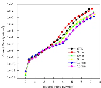
For both Al and Cu electrode samples, we have found that the leakage current is quite comparable before and after BTS. Hence, it is apparent that the electrode material has little impact on the leakage current characteristics. Furthermore, after O2 plasma treatment, the leakage current is decreased for both Al and Cu electrode. However, from the BTS current-time plot, we observe that the both Al and Cu electrode samples tend to breakdown in high electric field. In addition, the leakage current difference before and after BTS of Cu electrode sample is larger than that of Al electrode. Therefore, we can conclude that the resistance against Cu penetration of SiOC:H film is deteriorated after O2 plasma treatment even that its leakage current characteristics has been improved.
Furthermore, we are interesting in impacts of thermal annealing of the silicon carbide film, so the oxygen-doped silicon carbide film with Cu or Al metal gate was transferred into furnace at the temperature 400oC for 3 hours in N2 ambient is showed in Fig. 18 and Fig. 19. After thermal treatment electrical measurement will be also executed. MIS capacitors were used for the determination and evaluation of the permittivity of silicon carbide film. The current-voltage (I-V) characteristics measurements and bias-temperature-stress (BTS) measurement were also executed using MIS structure with HP4156 parameter analyzer. Fig. 20 is J-E cures of SiOC1,SiOC2, SiOC3 with Cu electrode after thermal annealing at RT. Fig. 21 to Fig. 23 is Current v.s Time curve of SiOC1, SiOC2, SiOC3 using Cu gate with intrinsic or after thermal annealing during BTS. The leakage current
would decrease after thermal annealing. Heating process will not degrade our silicon carbide films, but seem to eliminate the defects or dangling bonds in the films. Fig. 24 Current v.s. Time curve of SiOC1,SiOC2,SiOC3 with Cu gate after thermal annealing during BTS. Fig. 24 compare with Fig. 6. We will find thermal annealing cause reliability of silicon carbide films improved.
Leakage current behaviors of silicon carbide films can be investigated further on the J-E (leakage current density-electric field) characteristics such as ln(J) – E1/2 and
ln(J/E) – E1/2 plots. The linear variations of the current correspond either to Schottky-Richardson emission or to Poole-Frenkel mechanism. The Schottky-Richardson emission generated by the thermionic effect is caused by the electron transport across the potential energy barrier via field-assisted lowering at a metal-insulator interface. The current density (J) in the Schottky emission can be quantified by the following equation:
⎟⎟ ⎠ ⎞ ⎜⎜ ⎝ ⎛ − = T k E T A J B s s
φ
β
1/2 2 * exp (1) where 1/2 0 3/4 ) ( πε ε βs = e , e is theelectronic charge, ε0 is the dielectric constant
of free space, ε is the high frequency relative dielectric constant, A* is the effective Richardson constant, T is the absolute temperature, E is the applied electric field,
Фsis the contact potential barrier, and kB is the Boltzmann constant. The schematic of the energy diagram for Schottky emission is displayed in Fig. 25. Besides, the Poole-Frenkel (P-F) emission is due to field-enhanced thermal excitation of trapped electrons in the insulator into the conduction band. The current density is given by:
⎟⎟ ⎠ ⎞ ⎜⎜ ⎝ ⎛ − = T k E E J B PF PF φ β σ0 exp 1/2 (2)
where σ0 is the conductivity, E is the
electric field, 1/2
0
3/ )
( πε ε
βPF = e , and ФPF
is the height of trap potential well. The schematic of the energy diagram for Poole-Frenkel (P-F) emission is illustrated in Fig. 26. The barrier height, however, is the depth of the trap potential well, and the quantity βPF is larger than in the case of Schottky emission by a factor of 2. Distinction between the two mechanisms of leakage current can be done by comparing the theoretical value of β with the experimental one. The βS and βPF before and after BTS(4MV/cm) for SiOC1, SiOC2 and SiOC3 are listed in Tab. 3. The βS and βPF before and after BTS(4MV/cm) for SiOC1, SiOC2 and SiOC3 after thermal annealing are listed in Tab. 4. Besides, it can be approximately recognized from the symmetry or asymmetry on J-E curves. Because of the differences of work function and carrier concentration between gate and substrate materials, the J-E curves should be asymmetric in Schottky emission conduction. In other words, Schottky emission conduction is dominated by “electrode”. But carries in traps meet the same barrier height no matter in positive or negative bias. That is the reason why Poole-Frenkel emission shows a symmetric J-E curve and its behavior is dominated by “bulk”. Based on the above, we also can roughly determine the conduction mechanism by the symmetry about J-E curves.
The extraction procedure of experimental βs and βPF values are demonstrated on the left half court and right half court. For silicon carbide with Cu or Al gate, the slope (=β/kBT ) of the straight line portion of curves is showed in Fig. 27. We suppose that
there are many defeats and dangling bonds in silicon carbide films essentially and they will clutch and then release the carriers inject from electrode like “traps”. If carriers are held by traps, the carriers will form a build-in field against external field due to the Coulomb force. From the following equation:
2 1 2 1
)
(
idealE
E
Bβ
fitE
β
−
=
(3)βideal is the ideal value of βPF, βfit is the
experimental βPF exacted by fitting the ln(J/E) versus E1/2 plot, E is external field, and EB is build-in field. Therefore, (E-EB) which is shown in Fig. 28 is the actual field applied on insulator . If the quantities of traps increase, the EB will be enhanced and then let the value of βfit decrease. It is universally known that high temperature will let carriers jump out of the potential well easily. In another word, the release efficiency of traps will increase due to higher temperature. From the statistical viewpoint, the probabilities of carriers existing in traps decrease and then make the build-in field EB faint. We suppose that is the reason why we get a larger value of βfit at high temperature.
Furthermore, ψS is the contact potential barrier and ψPF is the height of trap potential well. For trap states with coulomb potentials, the expression is virtually identical to that of the Schottky emission. The barrier height is the depth of the trap potential well. In addition, we can calculateψS the contact potential barrier andψPF the height of trap potential well at high field. From Eq. (1) and Eq. (2), the current density is given as follow:
(4) (5)
We plotted ln(J) v.s. (1/T) and ln(J/E) v.s. (1/T). We can get the slope of the straight line
T k E E J B PF PF )1 ( ln ) ln( 2 1 0 Φ − + = σ β T k E k A J B s B s ) 1 ( * ln ) ln( = + β −Φ
portion of curve.
(6) (7)
The barrier height of SiOC1 was listed in Tab.
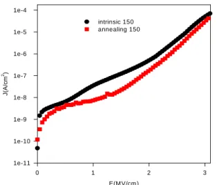
5. As shown in Tab. 6 , we found that βPF and ψPF of SiOC1 will increase after thermal annealing. Fig. 29 is J-E curve of SiOC1 before and after annealing with Cu gate at 150 . The leakage current decr℃ eased after annealing. According to Eq. (3), after thermal annealing, the quantity of traps might decrease and then lower the EB. We will obtain a large value of βfit. That could be the reason why we got a higher βfit value after thermal annealing. Moreover, the increase of the value of ψPF might caused by eliminating the shallower traps during thermal annealing and then make the average value of the height of traps potential well rise.
We found that βPF and ψPF of SiOC1 will increase after thermal annealing is shown in Tab. 7. Fig. 19 is J-E curve of SiOC1 before and after BTS with Cu gate at 150℃. The leakage current decreased after BTS. We will obtain a large value of βfit. According to Eq. (3), after BTS, the quantity of traps might decrease and then lower the EB.. That could be the reason why we got a higher βfit value after BTS. Furthermore, the increase of the value of ψPF might caused by eliminating the shallower traps during BTS and then make the average value of the height of traps potential well rise.
we let the sample break down during the bias-temperature-stress (BTS) measurement. Then, we put the sample into low temperature probe station and measure the current-voltage (I-V) characteristics.
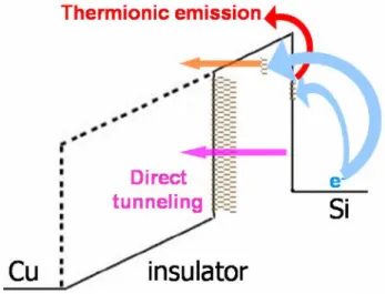
Fig. 30 to Fig. 32 show the leakage current density versus electric field (J-E) curve of SiOC1, SiOC2, SiOC3 measured at various temperature of 290OK, 200OK, 100OK with Cu electrode, respectively. From Fig. 30 to Fig. 32, the leakage current is very large both in
negative bias and positive bias after BTS. With the decreasing temperature, the leakage current was still very large in negative but was getting smaller in positive bias. The Cu ions existing in silicon carbide would be taken as trap states and could enhance the carriers to transport. The transport of carriers could be divided into three components as follows: thermionic emission, direct tunneling, and trap enhanced thermionic field emission. The third way includes trap enhanced thermionic emission and trap enhanced field emission ( indirect F-N tunneling).As shown in Fig. 33 and Fig. 34, the numerous trap states exist in insulator and cause the insulator barrier lowing. The insulator could be regarded as a combination of an ohmic conduction region(caused by numerous trap states exist in insulator) and a very thin insulator. Because of Cu penetration, the interface between ohmic conduction region and thin insulator has a lot of trap states. The electrons can easily transport from trap to trap and weakly depend on temperature. From Fig. 30 to Fig. 32, we can see the more oxygen in the film , the lower leakage current it is in negative bias at the low temperature. It is also show that the more oxygen in the film will has less trap states in the film.
四. 結論
A novel oxygen-doped silicon carbide (SiOC) films has been developed for barrier dielectric applications. The silicon carbide film is hydrophobic due to the existence of Si-CxHy bonds. It provides the silicon carbide a lower dielectric constant than that of typically used Six Ny (k~8) as a barrier dielectric and etch stop layer in the interconnection. From the electric analysis, we know that the more oxygen concentration in the film, the lower leakage current it is. It is presents that oxygen concentration in the film
B s S = E −slope×k Φ β B PF PF = E −slope×k Φ β
would prevent the Cu ion from diffusing into the film. The leakage current is like electron beam which impact the SiC film. The Si-C bond of SiC film is easier broken than Si-O bond. The Si-C break generate the traps which result in Cu diffusion. Therefore, the higher oxygen concentration has lower leakage current.
After O2 plasma treatment, the leakage current is decreased for both Al and Cu electrode. However, from the BTS current-time plot, we observe that the both Al and Cu electrode samples tend to breakdown in high electric field. In addition, the leakage current difference before and after BTS of Cu electrode sample is larger than that of Al electrode. Therefore, we can conclude that the resistance against Cu penetration of SiOC:H film is deteriorated after O2 plasma treatment even that its leakage current characteristics has been improved.
Than we know thermal annealing process would be a critical issue in BEOL fabrication process since the heat provided more possibility of the copper diffusion into low-k IMD & ILD. Therefore, we simulated the BEOL fabrication process by using thermal annealing. From electric analysis, we know the film after thermal annealing is better than intrinsic film. Because of thermal annealing recovered defeat of the film and caused leakage current decreasingly. The leakage current decreased as oxygen concentration increased in the film is still existence.
We suppose that there are many defeats and dangling bonds in silicon carbide films essentially and they will clutch and then release the carriers inject from electrode like “traps”. If carriers are held by traps, the carriers will form a build-in field against external field due to the Coulomb force. If the quantities of traps increase, the EB will be enhanced and then let the value of βfit decrease. It is universally known that high temperature
will let carriers jump out of the potential well easily. In another word, the release efficiency of traps will increase due to higher temperature.
After thermal annealing and BTS, the quantity of traps might decrease and then lower the EB. We will obtain a large value of βfit. That could be the reason why we got a higher βfit value after thermal annealing and BTS. Moreover, the increase of the value of ψPF might caused by eliminating the shallower traps during thermal annealing and then make the average value of the height of traps potential well rise.
Then we let the sample break down during the bias-temperature-stress (BTS) measurement. Then, we put the sample into low temperature probe station and measure the current-voltage (I-V) characteristics. From the electric analysis, the Cu ions existing in silicon carbide would be taken as trap states and could enhance the carriers to transport. Because of Cu penetration, the interface between ohmic conduction region and thin insulator has a lot of trap states. The electrons can easily transport from trap to trap and weakly depend on temperature. We can see the more oxygen in the film , the lower leakage current it is in negative bias at the low temperature. It is also show that the more oxygen in the film will has less trap states in the film.
五.參考文獻
[1] N. Awaya, H. Inokawa, E. Yamamoto, Y. Okazaki, M. Miyake, Y. Arita, and T. Kobayashi, “Evaluation of a Cu metallization process and the electrical characteristics of copper-interconnected quarter-micron CMOS,“ IEEE Trans. Electron Devices, 39, 1206-1212, (1996). [2] J. Tao, N. W. Cheung, and C. Hu,
“Electromigration characteristics of copper interconnects,“ IEEE Electron Devices
Lett., 14, 249-251, (1993).
[3] T. Lauinger, J. Moscchner, A. G. Aberle, and A. G. Hezel, “UV stability of highest-quality plasma silicon nitride passivation of silicon solar cells, “in Conf. Rec. 25th IEEE Photovoltaic Specialists Conf., 1996, pp. 413-419..
[4] S.M.Hu, “Properties of amorphous silicon nitride, “J. Electrochem. Soc.,vol. 33, pp. 693-698, 1966.
[5] V. Y. Doo, D. R. Nichols, and G. A. Silvery, “Preparation and properties of pyrolytic silicon nitride, “J. Electrochem. Soc., vol. 33, pp.1279-1281, Oct.1966. [6] J. O. Simpson, A. K. St. Clair, Thin Solid Film, 308, p.480 (1997)
[6] “The national technology roadmap for semiconductors, 1999 edition , ”
Semiconductor International Association, San Jose, CA, 1999.
[7] P. Xu, K. Huang, A. Patel, S. Rathi, B. Tang, J. Ferguson, J Huang, and C. Ngai, “BLOK—A low k dielectric barrier/etch stop film for copper damascene applications,” in Proc. IEEE Int. Interconnect Technol. Conf., 1999,pp. 109-111 [9] P. T. Liu, T. C. Chang, Y. L. Yang, Y. F. Cheng, and S. M. Sze, IEEE Trans. Electron Devices, 47, 1733 (2000) [8] E. Gat, M. A. El Khakani, M. Chaker, A.
Jean, S. Boily, H. Pepin, J. C. Kieffer, J. Durand, B. Cross, F. Rousseaux and S. Gugrathi, J. Mater. Res., 7 (1992) 2478. [9] A. L. S. Loke, C. Ryu, C. P. Yue, J. S. H.
Cho, and S. S. Wong, “Kinetics of copper drift in PECVD dielectrics,”IEEE electron device Lett. Vol. 17, p. 549-511, Dec. 1996 [10] The Application of plasma to chemical
Processing; Baddour, R. F.; Tim mins, R.
S., Eds.; Massachusetts Institute of
Technology Press: Cambridge, MA, 1967.
Tab. 1: Dielectric constant and refractive coefficient of SiC, SiOC1, SiOC2, SiOC3
Tab. 2: Dielectric constant, refractive coefficient and thickness of SiOC1 after O2 plasma treatment.
Tab. 3: βS and βPF before and after
BTS(4MV/cm) for SiOC1 3.1129 After BTS 4MV/cm 2.136 Before BTS 6.49 3.245 ideal SiOC3 4.652 After BTS 4MV/cm 2.389 Before BTS 6.442 3.221 ideal SiOC2 5.95 After BTS 4MV/cm 4.26 Before BTS 6.32 3.16 ideal SiOC1 βPF (x10-23) βS (x10-23) 150℃ 1.661 1.739 1.816 1.88 n 3.49 3.55 3.69 4.54 k SiOC3 SiOC2 SiOC1 SiC 961 956 943 956 984 984 Thickn ess(A) 2.024 2.013 1.966 1.882 1.879 1.816 n 3.87 4.01 3.95 3.74 3.89 3.69 k 15min 12min 9min 6min 3min STD
Tab. 4: βS andβPF before and after BTS(4MV/cm) for SiOC1, SiOC2 and SiOC3 after thermal annealing.
Tab. 5: ψbefore and after thermal annealing and after BTS for SiOC1
Tab .6: The changes on βPF and ψPF after annealing
Table 3-5 The changes on βPF and ψPF after BTS
Fig. 1: FTIR absorption spectra for SiC,SiOC1, SiOC2, SiOC3.
Binding energy (eV)
0 200 400 600 800 1000 1200 In te n s it y 0 2000 4000 6000 8000 Si 2s Si (SiO2) 2p C (C*-H) 1s O (SiO2) 1s C
Fig. 2:. XPS curve of intrinsic SiOC1.
3.683 After BTS 3MV/cm 2.611 Before BTS 6.49 3.245 ideal SiOC3 3.239 After BTS 3MV/cm 3.085 Before BTS 6.442 3.221 ideal SiOC2 6.221 After BTS 3MV/cm 5.131 Before BTS 6.32 3.16 ideal SiOC1 βPF (x10 -23 ) βS (x10 -23 ) 150℃ After 0.847(ev) After BTS ψ After annealing 0.72(ev) ψ After annealing 0.678(ev) ψ Before annealing 0.72 0.678 ΦPF 6.32 5.131 4.26 β (10-23) theoretical After Before 0.847 0.72 ΦPF 6.32 6.221 5.131 β (10-23) theoretical After Before Wavenumber (cm-1) 0 500 1000 1500 2000 2500 3000 3500 4000 4500 Absorbanc e (A.U .) Si-C Si-O Si-H SiC SiOC1 SiOC2 SiOC3 Si-CH3
Fig. 3: AES curve of intrinsic SiOC1
Fig. 4: J-E cures of SiC,SiOC1,SiOC2,SiOC3 with Al electrode at RT
Fig. 5: J-E cures of SiOC1 with Cu electrode at various temperature
Fig. 6:. Current v.s. Time curve of
SiOC1,SiOC2,SiOC3 with Cu gate during BTS
Fig. 7: FTIR of SiOC1 after 3min, 6min, 9min, 12min,15min O2 plasma treatment.
E(MV/cm) 0 1 2 3 4 J( A /c m 2) 1e-11 1e-10 1e-9 1e-8 1e-7 1e-6 1e-5 1e-4 1e-3 1e-2 1e-1 1e+0 SiC SiOC1 SiOC2 SiOC3 -4 -2 0 2 4 J( A /cm 2) 1e-11 1e-10 1e-9 1e-8 1e-7 1e-6 1e-5 1e-4 1e-3 RT 100 150 Time(sec) 0 200 400 600 800 1000 1200 I(A ) 1e-10 1e-9 1e-8 1e-7 1e-6 1e-5 1e-4 1e-3 SiOC1 5MV/cm SiOC2 5MV/cm SiOC3 5MV/cm W a v e n u m b e r ( c m- 1) 0 5 0 0 1 0 0 0 1 5 0 0 2 0 0 0 2 5 0 0 3 0 0 0 3 5 0 0 4 0 0 0 4 5 0 0 S i- C S i- O C -O S T D 3 m i n 6 m i n 9 m i n 1 2 m i n 1 5 m i n
Fig. 8: AES of SiOC1 after 6min O2 plasma treatment.
Fig. 9: AES of SiOC1 after 15min O2 plasma treatment. Temperature (oC) 0 200 400 600 800 1000 Rel a ti ve I n ten s it y 0 1 2 3 4 5 6 7 8 STD 3min 6min 12min 15min
Fig. 10: TDS (m/e=18) of B5-1 after O2 plasma treatment.
Fig. 11. C-V curve of SiOC1 after O2 plasma treatment. Electric Field (M V/cm ) 0 1 2 3 4 5 6 7 8 Cu rr e n t Den s ity (A /cm 2) 1e-12 1e-11 1e-10 1e-9 1e-8 1e-7 1e-6 1e-5 1e-4 1e-3 1e-2 1e-1 STD 3m in 6m in 9m in 12m in 15m in
Fig. 12: J-E curve of SiOC1 after O2 plasma treatment with Al electrode
Voltage (V) -30 -20 -10 0 10 20 30 Ca p a c it n c e ( p F ) 20 40 60 80 100 120 140 160 180 200 220 3min 6min 9min 12min 15min
Electric Field (MV/cm) 0 1 2 3 4 5 6 7 8 C u rre nt D ens ity (A /cm 2) 1e-12 1e-11 1e-10 1e-9 1e-8 1e-7 1e-6 1e-5 1e-4 1e-3 1e-2 1e-1 STD 3min 6min 9min 12min 15min
Fig. 13: J-E curve of SiOC1 after O2 plasma treatment with Cu electrode
Tim e (s) 0 200 400 600 800 1000 1200 Current (A) 1e-13 1e-12 1e-11 1e-10 1e-9 1e-8 1e-7 1e-6 1e-5 1e-4 1e-3 1M V /cm 2M V /cm 3M V /cm 4M V /cm 5M V /cm 6M V /cm 7M V /cm
Fig. 14: BTS of SiOC1 after 9min O2 plasma treatment with Al electrode.
Time (s) 0 200 400 600 800 1000 1200 Cur ren t (A) 1e-13 1e-12 1e-11 1e-10 1e-9 1e-8 1e-7 1e-6 1e-5 1e-4 1e-3 1MV/cm 2MV/cm 3MV/cm 4MV/cm 5MV/cm 6MV/cm 7MV/cm
Fig. 15: BTS of SiOC1 after 9min O2 plasma treatment with Cu electrode
Electric Field (MV/cm) 0 1 2 3 4 5 6 C u rrent Dens ity (A/cm 2) 1e-12 1e-11 1e-10 1e-9 1e-8 1e-7 1e-6 1e-5 1e-4 1e-3 1e-2 1e-1 STD 150oC STD R.T. 3min 150o C 3min R.T.
Fig. 16: J-E curve of Al electrode SiOC1 measured at 150oC and R.T. after 3MV/cm
stress with STD and 3min O2 plasma
Electric Field (MV/cm) 0 1 2 3 4 5 6 Current Dens ity (A/cm 2) 1e-12 1e-11 1e-10 1e-9 1e-8 1e-7 1e-6 1e-5 1e-4 1e-3 1e-2 1e-1 STD 150oC STD R.T. 3min 150oC 3min R.T.
Fig. 17: J-E curve of Cu electrode SiOC1 measured at 150oC and R.T. after 3 MV/cm
stress with STD and 3min O2 plasma
treatment.
Fig. 18: Schematic of damascene structure with Cu, low-k ILD IMD, barrier dielectric, etch stop layer and barrier metal after thermal annealing
Fig. 19: Show the experiment process
Fig. 20: J-E cures of SiOC1,SiOC2, SiOC3 with Cu electrode after thermal annealing at RT ILD IMD IMD ILD Metal Metal Barrier Dielectric Barrier Metal
Etch stop layer
Si SiOC Al Cu 5000A 1000A Si SiOC Al Cu 5000A 1000A
Thermal annealing
N2 400℃ 3hours
E(MV/cm) -4 -2 0 2 4 J(A/cm 2) 1e-11 1e-10 1e-9 1e-8 1e-7 1e-6 1e-5 1e-4 1e-3 1e-2 SiOC1 SiOC2 SiOC3Fig. 21: Current v.s Time curve of SiOC1 using Cu gate with intrinsic or after thermal annealing during BTS
Fig. 22: Current v.s Time curve of SiOC2 using Cu gate with intrinsic or after thermal annealing during BTS
Fig. 23: Current v.s Time curve of SiOC3 using Cu gate with intrinsic or after thermal annealing during BTS
Fig. 24: Current v.s. Time curve of SiOC1,SiOC2,SiOC3 with Cu gate after thermal annealing during BTS
time(sec) 0 200 400 600 800 1000 1200 I( A) 1e-7 1e-6 1e-5 1e-4 1e-3 anneal 4MV/cm anneal 5MV/cm intrinsic 5MV/cm intrinsic 5MV/cm time(sec) 0 200 400 600 800 1000 1200 I(A ) 1e-10 1e-9 1e-8 1e-7 1e-6 1e-5 1e-4 1e-3 anneal 4MV/cm anneal 5MV/cm intrinsic 4MV/cm intrinsic 5MV/cm time(sec) 0 200 400 600 800 1000 1200 I( A) 1e-11 1e-10 1e-9 1e-8 1e-7 1e-6 1e-5 1e-4 1e-3 anneal 4MV anneal 5MV intrinsic 4MV intrinsic 5MV time(sec) 0 200 400 600 800 1000 1200 I( A) 1e-11 1e-10 1e-9 1e-8 1e-7 1e-6 1e-5 1e-4 1e-3 SiOC1 5MV/cm SiOC2 5MV/cm SiOC3 5MV/cm
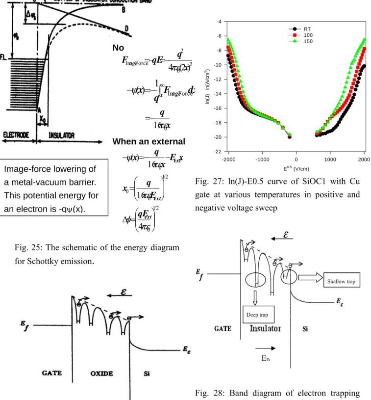
Fig. 25: The schematic of the energy diagram for Schottky emission
.
Fig. 26: The schematic of the energy diagram for Poole-Frenkel emission
Fig. 27: ln(J)-E0.5 curve of SiOC1 with Cu gate at various temperatures in positive and negative voltage sweep
Fig. 28: Band diagram of electron trapping and build-in field
Deep trap
EB
Shallow trap Image-force lowering of
a metal-vacuum barrier. This potential energy for an electron is -qψ(x). No 2 / 1 0 2 / 1 0 0 0 4 16 16 ) ( ⎟⎟ ⎠ ⎞ ⎜⎜ ⎝ ⎛ = ∆ ⎟⎟ ⎠ ⎞ ⎜⎜ ⎝ ⎛ = − − = − πε φ πε πε ψ ext ext ext qE E q x x E x q x When an external
dx
F
q
x
)
1
x age(
=
−
∫
∞ Im Force−
ψ
x q 0 16πε
− = 2 0 2 Force Im ) 2 ( 4 x q qE Fageπε
− = − = E0.5 (V/cm) -2000 -1000 0 1000 2000 ln (J ) ln(A/cm 2) -22 -20 -18 -16 -14 -12 -10 -8 -6 -4 RT 100 150Fig. 29: J-E curve of SiOC1 before and after annealing with Cu gate at 150℃
E(MV/cm) -2 -1 0 1 2 J(A /cm 2) 1e-9 1e-8 1e-7 1e-6 1e-5 1e-4 1e-3 1e-2 1e-1 1e+0 1e+1 1e+2 290 200 100
Fig. 30: J-E cures of SiOC1 with Cu electrode at low temperature E(MV/cm) -3 -2 -1 0 1 2 3 J( A /c m 2) 1e-9 1e-8 1e-7 1e-6 1e-5 1e-4 1e-3 1e-2 1e-1 1e+0 290 200 100
Fig. 31: cures of SiOC2 with Cu electrode at low temperature.
E(MV/cm) -2 -1 0 1 2 J( A/ c m 2) 1e-10 1e-9 1e-8 1e-7 1e-6 1e-5 1e-4 1e-3 1e-2 1e-1 1e+0 1e+1 1e+2 290 200 100
Fig. 32: J-E cures of SiOC3 with Cu electrode at low temperature E(MV/cm) 0 1 2 3 J(A /c m 2) 1e-11 1e-10 1e-9 1e-8 1e-7 1e-6 1e-5 1e-4 intrinsic 150 annealing 150
Fig. 33: Band diagrams of the leakage behavior of SiOC (breakdown) in negative voltage sweep.
Fig. 34: Band diagrams of the leakage behavior of SiOC (breakdown) in positive voltage sweep