316 IEEE ELECTRON DEVICE LETTERS, VOL. 16, NO. 7, JULY 1995
Low-Temperature Processed
MOSFET’
s with
Liquid Phase Deposited
SiO2-,F,
as Gate Insulator
Ching-Fa Yeh, Shyue-Shyh Lin, and Tzy-Yan Hong
Abstract-Device performances of MOSFET’s with Si02-zFz
gate oxides prepared by an extremely low-temperature (15” C) liquid phase deposition (LPD) method were investigated. The electrical characteristics, including threshold voltage of 2.1 V, peak effective mobility (pee) of 525 c m 2 N . s, and subthreshold swing of 134 mV/decade, show the devices exhibit comparable performance to other low-temperature processed MOSFET’s. This demonstrates that LPD SiOZ-zFz can be a suitable can- didate for future gate insulators in low-temperature processed MOSFET’s.
I. INTRODUCTION
URRENT demand for reduced device dimensions, and
C
increasingly complex device structures, have stressed the need for low-temperature processing1
11-15], while high- temperature processing can redistribute impurities and thus generate defects. This is especially true during MOSFET gate oxide formation where many defects in high-temperature ther- mally grown Si02 film are responsible for early breakdowns[6], 171. To date, a few MOSFET studies have looked at deposition of gate oxide at low temperatures [2]-[5]. Although they demonstrated some benefits, some of the methods still required high-temperature post-deposition treatment to im- prove device performance 121, [4]. In addition, all needed expensive apparatus and complex processing to prepare the low-temperature gate oxide.
Recently, a novel room-temperature liquid phase deposition (LPD) technique using inexpensive apparatus was developed for silicon oxide (SiO2-,F,) [8], 191, where the fluorine
will be naturally incorporated into the film during deposition. The LPD Si02-,FZ also showed comparable performance of breakdown field and leakage current to other low-temperature prepared oxides. Because it had been reported that the fluorine incorporated in the MOSFET gate oxide evidently improves the interface characteristics and increases immunity to hot- electron induced stress [10]-[12]. Thus, we were interested in applying this low-temperature SiO2-,F, processing method to MOSFET gate insulators. This paper presents the electrical characteristics of MOSFET’s made with such a new LPD gate oxide, and compares them with those of other types of low-temperature processed MOSFET’s.
Manuscript received November 30, 1994; revised April 14, 1995. This work was supported by the National Science Council, Republic of China, under Contract NSC-83-0404-E-009- 12 1.
C.-F. Yeh, S . 4 . Lin, and T.-Y. Hong are with the National Chiao Tung University, Department of Electronic Engineering and Institute of Electronics, Hsinchu 300, Taiwan, Republic of China.
IEEE Log Number 9412362.
1 0.8 0.6 0.4 0.2 0 0 1 2 3 4 Drain Voltage VD (V) (a) 10-1
,
10-3a
n
10-5F
10-7 h W-
+ c 3 L 10-9.-
E
n
lo-ll i 0-1 3 LPD Si02.xFx / \ p-substrateW
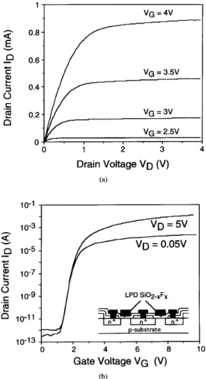
. _ 0 2 4 6 8 10 Gate Voltage VG (V) (b)Fig. 1. The typical (a) ID-VD, and (b) I D - V , characteristics of MOSFET’s with LPD SiOZ-,F, gate oxide. The inset in (b) shows the cross-sectional view of the fabricated device.
11. EXPERIMENTAL
N-channel MOSFET’s with aluminum gates were fabricated on 1-5 R.cm, (loo), p-type silicon substrates. A typical cross- sectional view of the fabricated device is shown in the inset of Fig. l(b). The channel length ( L ) and channel width ( 2 ) are 20 pm and 942 pm, respectively. The fabrication used conventional four-mask processes without channel implanta- tion. 100 nm-thick LPD Si02-,FZ formed at 15°C was first
YEH et al.: LOW-TEMPERATURE PROCESSED MOSFET's 500
-
450-
3176
o
o
;
i
550 aI
a a PFE m a a a 400 0 2 4 6a
10 VG-VT (V) Fig. 2.V&VT of MOSFET's with LPD gate oxide.
Effective mobility ( p , ~ ) and field-effect mobility FE) versus
used as gate insulator. Specifics concerning the deposition process of LPD oxide were the same as those in our previous works [8], [9]. Because the fluorine disappeared and the film became denser as the LPD Si02-zFz was treated at a temperature over 7OOOC [8], the processing temperature had to be carefully controlled to avoid affecting the LPD oxide.
So in our MOSFET processes, thermal diffusion of phosphorus
for the source and drain regions was adopted and performed before gate oxide deposition. In addition, we adopted an aluminum gate to replace the polycrystalline silicon gate, because aluminum evaporation has hardly any thermal effect on LPD oxide. Post-metal annealing at 4OOOC was the only high temperature process used after LPD oxide deposition. The resulting MOSFET electrical characteristics, such as drain- current ( I D ) versus drain-voltage (VD) or gate-voltage (VG) were measured, and the device parameters including threshold voltage (VT), subthreshold swing ( S ) , and mobility ( p ) were all analyzed. The interface state density (Dit) was also inves- tigated with MOS capacitors by high-frequency method [ 131.
111. RESULTS AND DISCUSSION
An Auger electron spectroscopy (AES) depth-profile of LPD oxide film has revealed that fluorine is uniformly distributed in the film [14]. The mechanism of fluorine incorporation has also been proposed [14]. Fig. l(a) shows the typical ID-VD characteristics of our MOSFET with VG varied in the range from 2 V to 4 V in 0.5 V steps. The ID-VD curve exhibiting triode characteristics and current saturation phenomena well, reveals a typical drain characteristic for a long-channel MOSFET. Because there is no current flowing at V, = 2 V, we know that the V, will be larger than 2 V. With accurate plotting of transconductance (gm) versus VG, the 2.1 V of VT was obtained to confirm the above result. The fact that this value of V, is lower than the 4 V of in other
studies [2] indicates that there are fewer fixed oxide charges contained in the LPD oxide. The typical 10-V~ characteristics of our MOSFET with VD = 0.05 V and 5 V, are also shown in
TABLE I
SUMMARIES OF DEVICE PERFORMANCES FOR MOSFET's
UTILIZING VARIOUS GATE OXIDE DEPOSITION METHODS
LPD gate @-AI Spurter- PECVD gate
oxide deposited gate oxide oxide [SI t21
Gate electrode Aluminum Polysilicon Aluminum
DepCs1uon telnpzlture 2 0 T 200°C 350°C
Post-annealing 400'C 800°C 400°C
Temperature
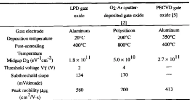
Midgap Dit (eV-lcm?) 1.8 x IO" 5.0 x 2.7 x IO"
2 4 Threshold voltage VT (V) - I34 170 - Subthreshold slope (mV/decade) 580 700 413
Fig. l(b), shown the drain current varies exponentially with VG in the subthreshold region. And the curves in the subthreshold region show virtually no dependence on the drain voltage. The peak transconductance calculated at V, = 0.05 V is
3.68 x s. Moreover, the subthreshold slope calculated from the 10-V~ curve is 134 mV/decade, which reveals superior to the 170 mV/decade recorded in other studies [2]. Although above results shows that our devices exhibit worse electrical characteristics than those conventional ones with thermal oxide, they exhibit comparable performance to other low-temperature processed MOSFET's.
Since the MOSFET mobility is strongly influenced by the surface states at or near the interface and by the morphology of Si/SiOz interface, it is essential to evaluate the mobility when investigating the interface quality. Fig. 2 shows the effective mobility ( p , ~ ) and field-effect mobility @FE) versus the VG-VT. The p e ~ and the FE are given by peff =
respectively, where 90 is the channel conductance, CO, is the gate capacitance per unit area. The mobility curves are highly consistent with those of MOSFET's with thermal gate oxide [15]. The peak p e f f is 525 c m 2 N
.
s, while the peakFE is 580 c m 2 N
.
s. The FE is lower than peff over almost the entire gate voltage region, because the derivation of FEneglects the dependence of gate voltage [16]. The fact that mobility decreasing with gate voltage can be attributed to the enhanced surface roughness scattering with increased gate voltage [15]. In comparison with other words, our peak FE is larger than 413 c m 2 N . s [5] but is less than 700 c m 2 N . s [2] of other works. These results show that the interface properties of Si/LPD Si02-,Fz are superior to those of SiPECVD Si02 but inferior to those of S d 0 2 - k sputter-deposited oxide. As compared in Table I, the DEt of our device is lower than that of sputtered oxide device, but higher than that of PECVD oxide device. The least Dit for the sputter-oxide device may be attributed to a high-temperature annealing, which was performed at 800OC after oxide deposition. And our devices having less Dit may be due to fluorine incorporation. It is because fluorine can passivate some interfacial dangling bonds, as well as remove some weak Si-Si or Si-0 bonds, via Si-F formation [lo]. However, it is impossible to directly prove the fact because we can not prepare any LPD oxide without fluorine incorporation. It is expected that the reliability of our
318 IEEE ELECTRON DEVICE LETTERS, VOL. 16, NO. 7, JULY 1995
devices will show better than other devices without fluorinated gate insulator. The study has been in progress.
IV. CONCLUSION
We have applied a novel room-temperature LPD Si02-zF, to low-temperature processed MOSFET without high-temper- ature annealing. Its 10-V~ and ID-& curves exhibit excel- lent triode-like characteristics and subthreshold characteristics, respectively. All the device parameters were compared well to those of other low-temperature processed MOSFET’s. These results reveal the great possibility of applying LPD Si02-zFz as a gate insulator in low-temperature processed MOSFET’s in the future.
REFERENCES
D. A. Baglee, “A review of recent developments in thin gate dielectric for VLSI,” J. Vac. Sci. Technol. A, vol. 4, p. 1002, 1986.
S. Suyama, A. Okamoto, and T. Serikawa, “Electrical characteristics of
MOSFET’s utilizing oxygen-argon sputter-deposited gate oxide films,”
IEEE Trans. Electron Devices, vol. ED-34, no. IO, p. 2124, 1987.
J. Stasiak, J. Batey, and E. Tierney, “Fabrication of thin gate MOSFET’s using low-temperature plasma-enhanced chemical-vapor-deposited SiO2,” IEEE Trans. Electron Devices., vol. ED-34, no. 11, p. 2367, 1987.
J. Lee, 1.X. Chen, and C. Hu, “Electrical characteristics of MOSFET’s using low-temperature chemical-vapor-deposited oxide,” IEEE Electron
Device Lett., vol. 9, no. 7, p. 324, 1988.
J. Stasiak, J. Batey, E. Tierney, and J. Li, “High-quality deposited gate
oxide MOSFET’s and the importance of surface preparation,” IEEE
Electron Device Lett., vol. IO, no. 6, p. 245, 1989.
K. Yamabe and K. Taniguchi, “Time-dependent dielectric breakdown of thin thermally grown Si02 films,” IEEE Trans. Electron Devices., vol. ED-32, no.
i,
j.
423, 1985.H. Abe. F. Kivosumi, K. Yoshioka, and M. Ino, “Analysis of defects in thin Si02 theimally grown on Si substrate,” in IEDM-Tech. Dig.,1985, p. 372.
C. F. Yeh, S. S. Lin, C. L. Chern, and Y. C. Yang, “Novel technique for
Si02 formed by liquid-phase deposition for low-temperature processed polysilicon TlT,” IEEE Electron Device Lett.. vol. 14, p. 403, 1993. C. F. Yeh, S. S. Lin, T. Z . Yang, C. L. Chern, and Y. C. Yang, “Performance and off-state current mechanisms of low-temperature processed polysilicon thin-film transistors with liquid phase deposited Si02 gate insulator,” IEEE Trans. Electron Devices, vol. 41, p. 173, 1994.
D. N. Kouvatsos, F. A. Stevie, and R. J. Jaccodine, “Interface state density reduction and effect of oxidation temperature on fluorine in- corporation and profiling for fluorinated metal oxide semiconductor capacitors,” J . Electrochem. Soc., vol. 140, p. 1160, 1993.
P. J. Wright and K. C. Saraswat, “The effect of fluorine in silicon dioxide gate dielectric,” IEEE Electron Devices, vol. 36, p. 879, 1989. Y. Nishioka, Y. Ohji, K. Ohyu, T. P. Ma, K. Mukai, and N. Natuaki, “Hot-electron hardened Si-gate MOSFET utilizing F implantation,”
IEEE Electron Device Lett., vol. IO, p. 141, 1989.
E. H. Nicollian and J. R. Brews, MOS (Metal Oxide Semiconductor)
Physics and Technology.
C. F. Yeh, C. L. Chen, and G. H. Lin, ‘The Physicochemical properties and growth mechanism of oxide (SiOz-,F,) by liquid phase deposition with H 2 0 addition only,” J. Electrochem. Soc., vol. 141, p. 3177, 1994.
S. C. Sun and J. D. Plummer, “Electron mobility in inversion and
accumulation layers on thermally oxidized silicon surface,” IEEE Trans.
Electron Devices, vol. ED-27, no. 8, p. 1497, 1980.
J. S. Kang and D. K. Schroder, “Effective and field-effect mobilities in
Si MOSFET’s,” Solid-State Electron., vol. 32, no. 8, p. 679, 1989. New York: John Wiley, 1982.