國
國
國
國
立
立
立
立
交
交
交
交
通
通
通
通
大
大
大
大
學
學
學
學
電子工程學系 電子研究所碩士班
碩 士 論 文
適用於超寬頻無線通訊之高速五階轉導-電
容濾波器設計
A High Speed Fifth Order Gm-C Filter
For Ultra-wideband Wireless Applications
研 究 生:楊富昌 Fu-Chang Yang
指導教授:溫瓌岸 博士 Dr. Kuei-Ann Wen
溫文燊 博士 Dr. Wen-Shen Wuen
適用於超寬頻無線通訊之高速五階
轉導-電容濾波器設計
A High Speed Fifth Order Gm-C Filter
For Ultra-wideband Wireless Applications
研 究 生:楊富昌 Student:Fu-Chang Yang
指導教授:溫瓌岸 博士 Advisor:Dr. Kuei-Ann Wen
溫文燊 博士 Dr. Wen-Shen Wuen
國立交通大學
電子工程學系 電子研究所碩士班
碩士論文
A Thesis
Submitted to Department of Electronics Engineering & Institute of Electronics College of Electrical Engineering and Computer Science
National Chiao Tung University In Partial Fulfillment of the Requirements
for the Degree of Master
in
Electronic Engineering
June, 2005
HsinChu, Taiwan, Republic of China
中華民國 九十四年六月
適用於超寬頻無線通訊之高速五階
適用於超寬頻無線通訊之高速五階
適用於超寬頻無線通訊之高速五階
適用於超寬頻無線通訊之高速五階
轉導
轉導
轉導
轉導-
--
-電容濾波器設計
電容濾波器設計
電容濾波器設計
電容濾波器設計
學生:楊富昌 指導教授:溫瓌岸 博士
溫文燊 博士
國立交通大學
電子工程學系 電子研究所碩士班
摘
摘
摘
摘
要
要
要
要
本論文完成一適用於超寬頻無線通訊之濾波器設計,以五階 elliptic 低通濾 波器來達成最窄的過渡頻帶(transition band),整個濾波器是用轉導、電容組成並 採取低敏感度的 LC 階梯型電路,其中轉導電路使用對稱及非對稱差動對來改善 線性度,以及負電阻技巧來增加差模輸出電阻,濾波器之全諧波失真(Total Harmonic Distortion)在 0.52V 峰對峰訊號下有-40dB,輸入相關雜訊電壓為 211.8uVrms,當考慮 20MHz 輸入訊號時,動態範圍(Dynamic Range)為 58.4 dB, 消耗的功率在 1.8-v 的供應電壓下為 32.25mW 其中包括 12.1mW 的輸出緩衝器, 質優值(Figure-of-Merit)為 59.75dB,此設計是以聯電 0.18 微米製程來實現, 為了方便量測,整個電路是採用矽品所提供之 QFN 系列包裝,並以印刷電路板做 為量測模組,量測結果頻寬為 226MHz,增益為-4.07dB 通帶起伏(ripple)為
High Speed Fifth order Gm-C Filters
For Ultra-wideband Wireless Applications
Student:Fu-Chang Yang Advisor:Dr. Kuei-Ann Wen
Dr. Wen-Shen Wuen
Department of Electronics Engineering
Institute of Electronics
National Chiao Tung University
Abstract
A 5th order CMOS high frequency elliptic low pass filter is designed to achieve narrowest transition band. The filter is composed of Gm blocks and capacitances. The symmetrical & unsymmetrical differential pair increases Gm linearity, and negative impedance increases Gm differential output resistance. The total harmonic distortion (THD) of this filter is -40dB within 0.52Vp-p. Input-referred noise is 211.8uVrms. Dynamic range is 58.4dB for 20MHz input. The power consumption of filters is 32.25mW (include 12.1mW output buffer) from 1.8V supply. The figure-of-merit for the filter is 59.75dB. The filter is implemented in UMC 0.18-μm CMOS technology and has been packaged in SPIL QFN20 which is mounted on PCB board in favor of measurement. The f3db is 226MHz and gain is -4.07 dB with 1.32 dB passband ripple.
誌 謝
很高興能夠順利完成這篇畢業論文,我要感謝我的指導教授溫瓌岸博士,在 求學態度及研究問題的方法上對我的教導,使我獲益良多,並且提供豐富的研究 資源來幫助我的研究,使得這篇論文能夠順利如期的完成。此外我也很感謝高曜 煌教授、詹益仁教授與陳巍仁教授能撥冗擔任我的口試委員,耐心聆聽與指教, 並提供寶貴意見,使得本論文得以更加完整。 感謝實驗室溫文燊學長、周美芬學姊、陳哲生學長和鄒文安學長等人提供我 在量測以及學業上指導,讓我受益良多。感謝在實驗室和同學建銘、兆鈞、格輝、 相霖、晧名彼此地討論,以及和學弟志德、俊憲、振威、懷仁、書瑋、彥凱互相 砥礪,讓研究生涯充滿歡樂與回憶。 還有我要感謝的是聯華電子公司、矽品精密工業、新復興微波通訊和所有幫 助過我順利生產、量測晶片的人。若不是有這麼多人的幫助,這篇論文不可能如 期完成,在此我誠摯地對這些幫助過我的人表達我的謝意。 最後我要感謝我的家人,他們無怨無悔的付出與鼓勵,使我求學過程中無後 顧之憂,僅以此論文與我的家人及好友分享我的收穫與喜悅,願他們永遠平安、 順心。 誌于 2005 楊富昌Contents
Abstract…..………..………...I
致謝………..……..………..………...III
Contents….………..………... IV
List of Tables………..………..…VIII
List of Figures………..……….…………..IX
Chapter1.
Introduction
...1
1.1 Motivation... 2
1.2 Specification...3
1.3 Organization...4
Chapter2.
Overview of High Frequency Filters
………...5
2.1 Terminology...………...5
2.2 Elliptic Filter Realization………....…………9
2.2.1 Active RC Filter
……….………...………9
2.2.2 Switched-Capacitor Filter
…………...…………..………10
2.2.3 MOSFET-C Filter
………11
Chapter3.
Transconductor analysis and design
……….………...15
3.1 Linearity analysis of differential pairs……...………...…….15
3.1.1 Square-law I-V relation……….…………..…………...
15
3.1.2 Body effect……….……
18
3.1.3 Mobility degradation from vertical field………….………...
19
3.1.4 Short Channel effect……….………..
20
3.2 Noise Analysis of a differential pair………..……21
3.3 Linearization Techniques for gm cells……….…….…….22
3.3.1 Source degeneration………...……
22
3.3.2 Adaptive biasing………..…….……..
23
3.3.3 Cross-Coupling………..……
26
3.3.4 Compensation using unbalance differential pairs……..………
28
3.3.5 Symmetric and un-symmetric differential pairs………...…………..
29
3.4 High Output Impedance Technique for gm cells………..……….31
3.4.1 Cascaded High Rout Element………...…..
32
3.4.2 Negative Impedance Load (NRL)………..……
32
3.5 Symmetric & un-symmetric pairs with NRL………….…………34
Chapter4.
Filter Analysis & Implementation……….….….…..
39
4.1 LC ladder filter………. ……….……….39
4.2 Element Replacement……….………40
4.3 Sensitivity………...47
Chapter5.
Filter Implementation and measurement………….……..
52
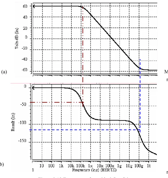
5.1 Simulation Result………..52
5.2 Circuit Layout………57
5.3 Package and Measurement Plane………...…...59
5.4 Measurement Result and Complarison………..64
5.4.1 Magnitude Response
……….……….……….64
5.4.2 Harmonic Distortion
……….………..66
5.4.3 One dB compression point
………...………….69
5.4.4 Comparison
………...………70
Chapter6.
Conclusions and Future work
………….……….….72
6.2 Future work………73
Appendix A
Symmetric & Un-symmetric Differential Pair...
……..78
Appendix B
LC Ladder analysis……….
………..…..………..….85
Reference
……….………..89
LIST OF TABLES
Table 3-1 Table of comparisons of various gm cells……….……….31
Table 5.1 Gm integrator comparison with specification………..53
Table 5.2 Filter comparison with specification………56
Table 5.3 Comparison with other filters………..57
Table 5.4 Harmonic Distortion Analysis……….68
Table 5.5 Filter comparison with specification.………...70
LIST OF FIGURES
Figure 1.1 Proposed UWB transceiver block diagram………...………2
Figure 1.2 Overview of some publication on continuous-time analog monolithic filters……..3
Figure 1.3 Specification of TX path………...……….……4
Figure 1.4 Specification of RX path…...………4
Figure 2.1 Comparisons with 5th LPF filter at same cutoff frequency………6
Figure 2.2 Frequency response of an ideal 5th order elliptic low-pass filter…………...………7
Figure 2.3 Pole-zero plots for a 5th order elliptic low-pass filter………8
Figure 2.4 3rd order elliptic low-pass filter using SAB (single amplifier biquad)………...9
Figure 2.5 3rd order elliptic low-pass filter using Switch Capacitor (SC) filter………10
Figure 2.6 3rd order elliptic low-pass filter using MOSFET-C filter……….11
Figure 2.7 Gm. (a) Symbol. (b) Equivalent circuit of ideal OTA………..12
Figure 2.8 the 3rd order elliptic low-pass filter using Gm-C filter..………...13
Figure 3.1 A source coupled differential pair………...16
Figure3.2 The noise source of a differential pair……….……….21
Figure3.3 Source degeneration technique……….22
Figure3.4 Adaptive bias degeneration………..23
Figure3.5 Cross-coupling gm cell……….26
Figure3.6 Unbalance differential pairs………….……….28
Figure3.7 Symmetric & un-symmetric pairs……….29
Figure 3.8 Cascoded 2nd stage to improve Rout………32
Figure3.11 Symmetric & un-symmetric with NRL………...35
Figure3.12 non-ideal Gm-C integrator………..36
Figure 3.13 Frequency of non-ideal Gm-C integrator………..………37
Figure 4.1 the 5th elliptic LC ladder………..39
Figure 4.2 Differential Gm connected as resistance……….41
Figure 4.3 Differential Gm connected as inductance by gyrator approach………...41
Figure 4.4 resistor implemented by non-ideal Gm with finite 1/go and bandwidth………….41
Figure 4.5 Inductor implemented by non-ideal Gm with finite (a) Rout (b)RHP-zero..……..42
Figure 4.6 Non-ideal Gm effects the inductor………..…43
Figure 4.7 Negative impedance at DC……….……….44
Figure 4.8 LC ladder low frequency gain with negative impedance………44
Figure 4.9 the 5th elliptic ladder filter using Gm-C technique………..45
Figure 4.10 Adjust gm value in gyrator………46
Figure 4.11 after adjusting X & Y……….46
Figure 4.12 the 5th equal-ripple LC ladder filter using Gm-C technique………..47
Figure 4.13 the 5th elliptic LC ladder filter working between Rin and Ro……….50
Figure 5.1 Gm and Integrator simulation result………53
Figure 5.2 Buffer magnitude response………..53
Figure 5.3 the 5th elliptic low pass filter simulation result (post-sim)………...54
Figure 5.4 5th equal-ripple low pass filter simulation result (pre-sim)………...55
Figure 5.5 Transient & Harmonic Balance analysis with Vpeak=0.4V...……….55
Figure 5.6 Layouts of Gm and Buffer………...57
Figure 5.7 Symmetry layout………..58
Figure 5.8 Layout of 5th order elliptic low pass filter………59
Figure 5.11 Package pin assignment……….61
Figure 5.12 PCB Schematic………...62
Figure 5.13 PCB layout……….62
Figure 5.14 Measurement Plan………..………63
Figure 5.15 Magnitude Response………..64
Figure 5.16 Cutoff frequency measurement results……….…….65
Figure 5.16 Harmonic Distortion with 20 MHz input…………..……….65
Figure 5.17 magnitude response with -10dBm input (250kHz~20MHz)……….66
Figure 5.18 Spectrum and transient response with 0.4Vpeak input at 20MHz………66
Figure 5.19 Spectrum and transient response with 0.4Vpeak input at 200MHz……..………67
Figure 5.20 Measured spectrum and transient response with 0.4Vpeak input at 20MHz……67
Figure 5.21 Measured spectrum and transient response with 0.4Vpeak input at 20MHz……67
Figure5.22 One dB compression point (P1dB)………...69
Figure5.23 Noise figure analysis…………...………...71
Figure 6.1 Frequency tuning technique……….74
Figure 6.2 Quality tuning technique………...74
Figure 6.3 bias circuit using threshold compensation technique………..75
Figure 6.4 the filter magnitude response with four transistor corner cases………..75
Figure 6.5 after adding voltage threshold compensation biasing circuit………..76
Figure 6.6 LC ladder can be used to match complex load………77
Figure A.1 Cross-coupled quad cell………...78
Chapter 1
Introduction
Ultra-wideband (UWB) is a new wireless technology approved by Federal
Communications Commission (FCC) in US [1]. The IEEE 802.15.3a task group (TG3a) is
currently developing a UWB standard from the proposals submitted by different companies. It
is now left with two primary proposals, Multi-Band OFDM and Direct Sequence UWB.
Figure 1.1 shows Proposed UWB transceiver block diagram for MB OFDM system. TX and
RX both need filters to suppress unwanted high frequency spectrum. For this system, the
channel bandwidth has been extended to 528MHz. With such high frequency demand, the Gm
block is ubiquitous as filter element in communication system. Because the Gm has very high
bandwidth and well suits to high frequency filter design. Many commonly used MOS circuit
simulation even does not model an upper-frequency limit in the intrinsic conversion from
gate-source voltage to drain current (except gate-drain capacitance). Unless we consider non
quasi-static or gate-resistance effects, a high-frequency limit is hardly found [2]. The elliptic
low pass filter is preferred on account of high requirement for side-band suppression in UWB
specification, the nonlinear phase property of elliptic filter is not concerned. The newly
unlicensed UWB opens doors to wireless high-speed communications and has been exciting
tremendous academic research interest.
Figure 1.1 Proposed UWB transceiver block diagram
1.1 Motivation
The UWB MB-OFDM sets targets of low power consumption and low cost. The
complementary metal-oxide semiconductor (CMOS) technology is the best choice to make it
since the physical layer implemented in CMOS process consumes less power than others and
consequently has lower cost. The research goal of this thesis is to implement a high speed low
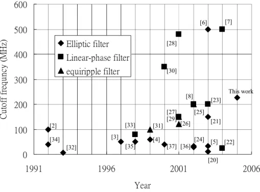
pass filter in CMOS technology for wireless UWB applications. A historical overview range
from 1992 of continuous-time filters is given in Figure1.2. This overview is not intended to be
complete but only gives an impression of the progress in analog CMOS continuous-time
filters. 0 100 200 300 400 500 600 1991 1996 2001 2006 Year C u to ff f re q u n cy ( M H z) Elliptic filter Linear-phase filter equiripple filter
Figure 1.2 Overview of some publications on continuous-time analog monolithic filters
1.2 Specification
Filters are classified according to the functions they are to perform. For anti-aliasing filter in UWB TX system, there needs a high frequency LPF to filter out D/A quantization noise. The D/A sample-rate is higher than Nyquist-Rate, so the specification of the LPF for TX path is relaxed. On the other hand, the side band frequency is very close to signal band for UWB RX system. The transmitter & receiver specifications are shown in Figure 1.3 and 1.4.
This work [5] [29] [25] [36] [20] [8] [21] [22] [24] [23] [26] [2] [3] [6] [7] [28] [30] [32] [33] [34] [35] [27] [31] [37] [4]
P as s iv e M ix e r B W= 3 - 1 0 G H z C on v G a in= - 1 0 d B P o ut, a v g= - 20 d B m P o ut, pe a k= - 1 0dB m D is trib u te d A M P B W = 3- 10 G H z G a in= 1 2 dB P o u t, av g=- 8 d B m P o u t, p e ak= 2 d B m O P1 d b= 5 d B m O IP3 = 1 5 d B m L T C C B P F B W = 3- 1 0 G H z P o ut, a v g= - 1 0 dB m P o ut, p e a k= 0 d B m L O 5 b it D A C 10 5 6 M H z L o w P o w e r( 4 0 m W) 5 th E llip tic L P F F3 d B = 2 4 5 M H z In- B a nd rip p le< 1 d B - 1 2 d B a t 26 0 M h z - 2 0 d B at 3 0 0 M h z
Figure 1.3 specification of TX path
5 bit ADC 528 MHz 5th Elliptic LPF F3 dB = 245 MHz In-Band ripple<1dB - 12 dB at 260 Mhz PGA Gain=25- 75 dB GainCtrl= 5bit BandGroup1 Mixer BW=3-5 GHz ConvGain= 0 dB NF= 8 dB BandGroup1 LNA BW=3-5 GHz Gain=25dB NF= 3 dB LTCC BPF BW=3- 10GHz Pout, avg=-10 dBm Pout, peak=0dBm - 20 dB at 300 Mhz
Figure 1.4 specification of RX path
1.3 Organization
The organization of this thesis is overviewed as following:
Chapter 2 gives some basic concept of high frequency filter design. Chapter 3 deals with transconductor analysis and design. High linear and high output resistance technique is introduced and the transconductor will be compared with other Gm of different linearity skills. Chapter 4 demonstrates the simulation of the proposed LC ladder filters by Gm-C topology. The high speed elliptic filter is implemented in 0.18µm CMOS technology and performs in post-simulation result in Chapter 5. In the same chapter the figure-of-merit is introduced to make a comparison with other filters. Chapter 6 concludes with a summary of contributions
Chapter 2
Overview Of High Frequency Filters
In this chapter, some fundamental concepts in the design of high frequency filters,
together with the frequency response of elliptic filters will be reviewed. Filters are classified
according to the functions they perform. Since our filters are designed for the UWB
receivers/transmitters, it will be focused on low pass filters in this thesis. In section 2.1, the
terminology of low pass filters is described. The circuit level implementation methods are
described in section 2.2.
2.1 Terminology
The LPF in the UWB receiving path is required to have sharp transition band with
minimum power constraint to filter out sideband noise. Figure 2.1 shows five types of 5th
order LPF filters with cutoff frequency at 250MHz for comparison. Elliptic (cauer) filters are
found to be the best choice owing to its ability to meet the stringent specification i.e. better
sharpness. Although elliptic filters have non-linear phase response as shown in Figure 2.1(b).
However, our design is targeted to a MB-OFDM UWB system, and the non-linear phase
-80 -70 -60 -50 -40 -30 -20 -10 0 10
1.62E+08 2.23E+08 3.08E+08 4.24E+08 Frequency (Hz) D el ay ( se c) bessel butter cheb1 inv.cheb ellitpic (a)Magnitude 0.00E+00 1.00E-09 2.00E-09 3.00E-09 4.00E-09 5.00E-09 6.00E-09 7.00E-09 8.00E-09 9.00E-09 1.00E-08
1.00E+08 1.38E+08 1.90E+08 2.62E+08 3.61E+08 4.98E+08 Frequency (Hz) D el ay ( se c) bessel butter cheb1 inv.cheb ellitpic (b)Group delay
The transfer function of a 5th order elliptic LPF is: 0 1 1 2 2 3 3 4 4 5 1 2 0 2
)
)(
(
)
(
β
β
β
β
β
α
α
+
+
+
+
+
+
+
=
s
s
s
s
s
s
s
A
s
H
(2.1)The transfer function has four pure imaginary zeros and five complex poles. The sharp
transition band is achieved and can be shortened by the existence of zeros in the stop band.
For very high frequency, the response sustains to reduce by one ahead of numerator:
(
)
→
when
s
→
∞
s
A
s
H
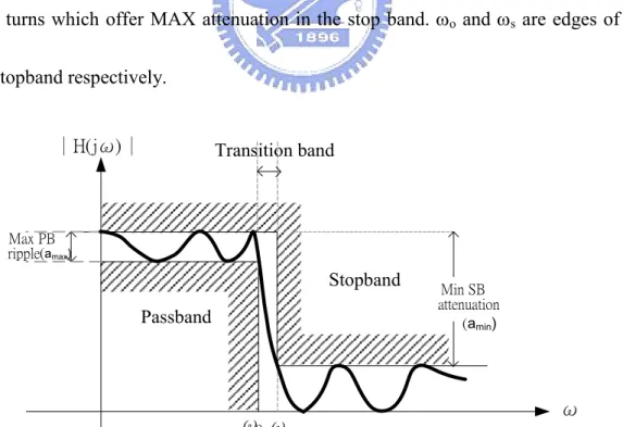
(2.2)Figure 2.2 shows the frequency response of an ideal 5th order elliptic low-pass filter. There’re five turns (fall-rise-fall-rise-fall) which causes ripples in the pass band. So are the same turns which offer MAX attenuation in the stop band. ωo and ωs are edges of passband
and stopband respectively.
Passband Stopband Transition band Min SB attenuation (amin) Max PB ripple (amax) ωo ωs ω ∣H(jω)∣
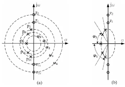
Figure 2.3 Pole-zero plots for a 5th order elliptic low-pass filter
Figure 2.3 shows pole-zero plots for the 5th order elliptic low-pass filter. The poles &
zeros are shown in frequency domain. “Elliptic filter” is called owing to all the poles lie in an
elliptic circle. The frequencies of poles & zeros can be obtained by their radiuses of Figure
2.3 (a). The quality factor of poles & zeros is obtained by the angle from each point to x-axis
in Figure 2.3 (b):
)
2
/
1
(
cos
1Q
i −=
ϕ
(2.3)The 5th elliptic LPF has zeros with very high Q (infinite in ideal case) locating in high
2.2 Elliptic Filter Realization
Several approaches have emerged to implement elliptic filters with different usages and
techniques. For simplicity, examples of the 3rd elliptic low pass filters are used in following
analysis. Among all the designs, our interests are mainly in the low power design.
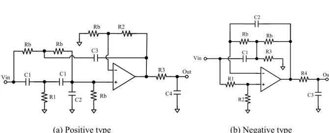
2.2.1 Active RC Filter
The active RC filter (using single amplifier biquad) is well-developed and shows in
Figure 2.4. In modern technology, accuracy resistance value is not easy to achieve due to
process variation. Another problem arising with high frequency is that active RC filters need a
high bandwidth amplifier. Moreover, this design uses a large amount of resistors which not
only consumes chip area, but also introduces noise.
Rb R1 Rb Vin Rb Out C3 Rb C4 R3 R2 C1 C1 C2 Rb R1 R2 Vin Rb Out C1 R3 C2 C3 R4
(a) Positive type (b) Negative type Figure 2.4 3rd order elliptic low-pass filter using SAB (single amplifier biquad)[17]
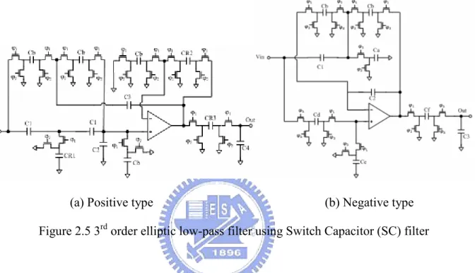
2.2.2 Switched-Capacitor Filter
In order to eliminate the process variation of resistors, another approach to implement 3rd
elliptic filter uses switched-capacitor (SC) to replace resistors as shown in figure 2.5.
(a) Positive type (b) Negative type
Figure 2.5 3rd order elliptic low-pass filter using Switch Capacitor (SC) filter
The design of SC filters follows fundamentally the active RC methods to obtain cutoff
frequency as mention above but avoids the use of real resistors. It relies on the fact that a
rapidly switched capacitor behaves like a resistor so that RC time constants are determined by
ratios of capacitors and by the clock frequency with which the capacitors are switched.
However, SC filter is not suitable in high frequency application. The main reason is
clock frequency limitation and finite Opamp settling time. A general rule of thumb is that the
clock frequency should be four to eight times higher than the input signal ωi. The finite
mainly focuses on finite OPamp unity-gain ωu (linear settling time) for simplicity. ωu should
be chosen more than five times of clock frequency, so that the Opamp has enough time to
settle. To avoid unnecessary noise aliasing and power dissipation, however ωu should be as
small as possible. For this reason, the SC filter is restricted for low frequency applications.
2.2.3 MOSFET-C Filter
Another closely related technique is MOSFET-C filters as shown in figure 2.6.
MOSFET-C filters are similar to fully differential active-RC filters, except resistors are
replaced by equivalent MOS transistors operationg in triode region. The transistors have
smaller process variation than resistors. However, the internal node signal swing could make
transistors leave triode region. And the transistor has parasitic capacitor which should be
considered. In next section, the gm-C filter which does not need Opamp will be introduced.
(a) Positive type (b) Negative type Figure 2.6 3rd order elliptic low-pass filter using MOSFET-C filter
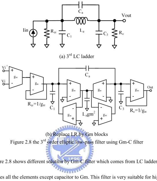
2.2.4 Transconductance-C Filter
The last method extends to applications at hundreds of megahertz by avoiding usage of
operational amplifiers and obtaining gain from transconductance amplifiers. The Gm
bandwidth can be achieved to tens of GHz and suitable for high frequency filter.
Transconductance amplifiers are voltage-controlled current sources (VCCS), Io=gmVi. This
method uses only Gm and capacitors and is referred to as the Gm-C method. The symbol of
ideal operational transconductance amplifier (OTA or Gm) is shown in figure 2.7(a). Fiugure
2.7(b) shows its equivalent small signal circuit. The finite input/output impedance and Gm
RHP-zero limitation cause non-ideal effect which will be analyzed in chapter 3. Since Gm is
very suitable for HF application, this thesis mainly rivets to Gm filters.
) (Vi+−Vi− gm ) (Vi+−Vi− gm
(a) 3rd LC ladder
(b) Replace LR by Gm blocks
Figure 2.8 the 3rd order elliptic low-pass filter using Gm-C filter
Figure 2.8 shows different solution by Gm-C filter which comes from LC ladder filter and replaces all the elements except capacitor to Gm. This filter is very suitable for high frequency filter and will be analyzed in chapter 4.
There are many synthesis methods to implement Gm filters. But not all methods are suitable for high frequency applications, since some of them have nodes without desired capacitance to ground [2]. If a node exits without grounded capacitances to absorb the parasitic capacitance, there will be deviations in the filter characteristic.
For good CMRR and low even order distortion, the Gm filters should be designed with differential topology Two synthesis methods are most common used topologies. They are
cascaded biquads and LC-ladder filters. Both of them have complementary properties.
Cascaded biquads are easy to develop but suffers from sensitivity. While LC ladder filter has
very low sensitivity to component variations in the pass band.
The frequency response of a filter is determined by the values of transconductance,
capacitance, and quality factor. To maintain an accurate filter response, precise absolute
values of components are necessary. Absolute values on an integrated circuit can shift
significantly from the nominal due to process parameter variations, temperature and aging. To
maintain a reasonable level of insensitivity of filter characteristics due to parameter shifts, a
system which corrects for these effects is required. Depending on the accuracy of response
Chapter 3
Transconductor analysis and design
Transconductor is the key element in CMOS Gm-C filters. Although Gm has linearity
problems, for high frequency application the resistor, inductor, and even VCOs need Gm to be
the key elements. In deep-submicron technique, nonlinearity problem gets worse with the
reduction of supply voltage. Linearity techniques are therefore, required. Several linearization
techniques to achieve better linearity of Gm cells will be investigated in Section 3.1 and the
corresponding noise will be compared through spice simulation. The negative impedance
method for higher quality factor will also be delivered in Section 3.2. Finally, the proposed
symmetric & un-symmetric differential pair with negative impedance will be discussed in
section 3.3.
3.1 Linearity analysis of differential pairs
3.1.1 Square-law I-V relation
When MOS device is operating in saturation regions, it follows the square-law relation
L
W
C
V
V
V
K
I
d gs t ds 0 ox 22
1
K
where
)
1
(
)
(
−
+
λ
=
µ
=
(3.1)The channel length modulation term (1+
λ
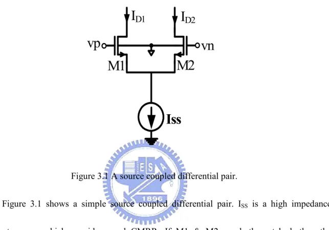
Vds) will cause an equivalent output impedance ro of MOS device.Figure 3.1 A source coupled differential pair.
Figure 3.1 shows a simple source coupled differential pair. ISS is a high impedance
current source which provides good CMRR. If M1 & M2 are both matched, then the
differential output current Iout = ID1- ID2 is given by [9]:
I
out=
2
K
(
V
gs−
V
t)(
vp
−
vn
)
(3.2)Where Vgs is common-mode gate-source voltage, ideally the value is constant. But
actually the source of M1& M2 is not perfectly virtual ground. When Vid = (vp-vn) is large, a
square term, Vid2 becomes significant in ID1+ID2:
]
2
)
(
2
[
2 2 2 1 id t gs D D ssV
V
V
K
I
I
I
=
+
=
−
+
(3.3)M1
Iss
M2
vp
vn
I
D1I
D2Because of the fixed current source Iss, the Vgs may change with Vid. The complete
expression of Iout is obtained as below:
≥ ≤ − = K I V I K I I K V K I V I ss id ss ss ss id ss id out id id 2 V when ) sgn( V en wh 2 1 2 2 1 (3.4)
The transconductance value can be estimated by (3.4) and used Taylor expansion to
analyze: ....) 2 2 3 2 ( 2 1 2 1 ) 1 ( 2 2 1 2 2 3 2 2 − − = − − = ∂ ∂ = id ss ss ss id ss id ss id out m V I K K I I K V I K V K I V I g (3.5)
From (3.5) gm reduces with the increase of Vid. And gm has a small signal
approximation value of 2IssK 2
1
3.1.2 Body effect
The sources of M1& M2 of the differential pair have a voltage difference VSB with
respect to the substrate in CMOS process. So the Vt of each transistor has to be modified as
[9]: F SB FB F F SB T T
V
V
V
F
V
V
=
0+
γ
[
+
2
φ
−
2
φ
]
=
+
2
φ
+
γ
+
2
φ
(3.6) ox SUB siC
N
q
ε
γ
=
2
(3.7)
Where Nsub is the doping concentration, εsi is the silicon dielectric constant, q is electron
charge, VFB is the flat-band voltage, φF is the difference between the Fermi level and the
intrinsic level and VTO is the original threshold voltage without body effect.
From the I-V relationship of (3.3), the body effect is considered and the VSB varies with
Vid. Then the non-linear characteristic of a differential pair is no longer a simple square-law
relation. This could affect the linearization techniques such as active biasing or unbalanced
gm cell that will be introduced later. For small signal amplitudes smaller than 100 mV, the
simple I-V relationship can still hold. Therefore, the linearization techniques using
3.1.3 Mobility degradation from vertical field
The mobility degradation of transistors worsens the complexity of the non-linearity
problem. A vertical field originating from the gate voltage exists and influences carrier
velocity. In deep submicron technology the increasing vertical electric field forces the carriers
in the channel closer to the surface of the silicon. The defected surface will reduce the
carriers’ movement. With the effect of mobility degradation, the drain current is modified as
follows: 2 0 2 D ) ( ) ) ( 1 ( 2 1 ) ( 2 1 I ox gs t t gs t gs ox eff V V L W C V V V V L W C − − + = − =
θ
µ
µ
(3.8)whereθ is the mobility degradation constant.
This is especially significant for short channel devices, because the gate oxide layer is
very thin. Thinner gate oxide means a stronger vertical field. In order to keep the same Vt,
higher doping of the substrate is implemented, which will reduce the channel effective
“thickness” and therefore further degrades carrier mobility.
Iss can be modified with mobility degradation as:
2 2 2 2 2 2 2 2 2 1 ) 2 ( )] ( 1 [ ] ) 2 ( 2 ) ( 2 )[ ( 2 ) ( 2 id t gs id id t gs t gs id t gs D D ss V V V V V V V V V V V V K I I I θ θ θ θ − − + − + − − + + − = + = (3.9)
The Vgs is a function of Vid. When taking mobility degradation into consideration, the
mobilities between M1 and M2 in the differential pair have large difference with larger Vid.
channel devices, which have thicker oxide and therefore smaller vertical field. However the
long channel device has large parasitic capacitance and doesn’t achieve high frequency
application. Another solution is to bias the transistors at a higher Vgs-Vt to gets maller
percentage variation of mobility.
3.1.4 Short channel effect
For short channel devices, the electric field between source and drain can reach the field
strength Esat at which the velocity of the channel carriers saturates. At high fields, the carrier
velocities approach the thermal velocities, and decreases with the increase of electric field.
The modified expression of ID with the pinch-off phenomenon is given as:
sat dsat t gs ox D
WC
V
V
V
v
I
=
(
−
−
)
(3.10) In (3.10) Vdsat is the Vds when the channel carriers achieve saturation velocity Vsat and is
given as: t gs eff t gs eff dsat
V
V
L
V
V
L
V
−
+
−
=
µ
µ
2
)
(
2
(3.11) where µeff is the effective mobility.In long channel device (3.10) can be simplified to be (3.1). In deep submicron devices,
the order of (Vgs-Vt) in (3.1) is less than 2. This does not mean that the device is more linear,
since the perfect linear relationship occurs at L=0..Furthermore, the Vdsat varies with Vgs-Vt.,
M1
Iss
M2
vp
vn
I
D1I
D2Load
The hot electron effects and drain-induced barrier lowering (DIBL) are also short
channel effects. Detailed analysis will be out of the scope of this thesis and thus not provided
here.
3.2 Noise analysis of a differential pair
Figure3.2 The noise source of a differential pair
In Figure 3.2 the Rout, Cout and Gm of M1 and M2 are the same in this calculation. For long
channel devices, the output noise Vn2 of each gm cell can be expressed as [9]:
]
3
8
[
2
2 2 out m nKTBg
R
V
=
γ
×
(3.12)
The noise power is doubled, because there are 2 branches. Note that the constant γ is 1
for long channel devices and with noiseless loading. However, the output loading has its own
noise. If short channel effects, such as hot electron effect of the long channel counterpart, are
3.3 Linearization Techniques for gm cells
There are many techniques implemented to reduce the variation of gm of differential pairs
with the high swing Vid. In the subsection, the source degeneration [10] [11], active biasing
[12], cross coupling [13], unbalanced differential pair [14], and symmetric & un-symmetric
differential [5] pair will be introduced respectively.
3.3.1 Source degeneration
(a) Source degeneration (b) Saturated transistor Figure3.3 Source degeneration technique
In Figure3.3 (a), the degeneration resistance can be changed dynamically with the input
signal amplitude. Qualitatively, when the amplitude of the input signal rises, the triode-mode
degeneration MOS resistors will be more biased to reduce the synthesized resistance and
provide less degeneration. The gm reduction from larger input signal is therefore compensated
)
4
/
(
1
1 3 1K
K
g
g
m m+
=
(3.13) where K is 0.5µnCoxW/L
The other technique using saturated transistor as degeneration resistor shown in Figure
3.3(b), the equivalent gm is [11]: 2 1 1
/
1
m m m mg
g
g
g
+
=
(3.14)
The rise of gm then compensates for the drop of gm expressed in Eq. (3.5). However, the
compensation is not adaptive. Therefore it is suitable when the range of tolerance of gm is
relatively large.
3.3.2 Active biasing
(a) (b) Figure3.4 Adaptive bias degeneration[12]
From (3.4) & (3.5), the nonlinear characteristic of differential pairs is observed to come
from the expression id
I K V 2 1 2
expression. The method is to make the biasing current compensation for the non-linear term: 2 2 id DC ss V K I I = +
(3.15) where IDC is the DC bias current.
Now the bias Iss supplies IDC when Vid = 0 for the static bias. When there is a signal, an
additional bias current KVid2/2 will compensate for the drop of the gm. This can be verified by
inserting the new Iss into Eq. (3.3):
DC t gs D D I K V V I I 1 + 2 =2 ( − )2 =
(3.16) As a result, a constant gm is obtained because Vgs-Vt of each input transistor is constant.
One of the designs is shown in Fig. 3.4(a).
In this design, all transistors are matched except M5-M8. For this cascoded circuit, when
there is an input signal, the same amplitude appears at the drains of M1 and M2 because the
loading is 1/gm3,4 and gm3,4=gm1,2. Here, ro1,2 >> 1/gm1,2 is assumed and the capacitance at that
node and the loss of the level shifter M5-M8 are ignored. Both gates of Mb1 and Mb2 sense the
differential voltage. Because the drains of Mb1 and Mb2 are connected together, a bias current is
obtained as in (3.2) and (3.15). The required active biasing is then established.
When the gm cell is used for high frequency applications, say 250 MHz, the capacitance
increase the voltage gain of M1 and M2. This ensures that the KVid 2/2 is enough to compensate
for the non-linearity.
The same linearization effect can be achieved by connecting the gates of Mb1 and Mb2 to
the 2 inputs respectively. But in the common-mode sense, now the conductance of Mb1 and
Mb2 increases in phase with the input signal. This is a kind of feed-forward and thus causes a
boost-up of the common-mode gain. As a result, CMRR drops and common-mode instability
will be resulted.
There is a modified design that can operate at a lower supply voltage. The schematic is
shown in Fig. 3.4(b). Instead of controlling the gate bias of the bias transistor Mb, a differential
pair M3-M6 acts as a bias current. Both pairs share the same bias current source.
When the signal amplitude is small, M3 and M4 are in saturation region while M5 and M6
are in triode region. M3-M6 drain out some of the bias current. When the signal amplitude is
positive and large, M6 will go into saturation region and M5 will be cut off. Smaller sum of the
bias current will be drained out by M3-M6. That means more current will be supplied to M1
3.3.3 Cross-coupling
Figure3.5 Cross-coupling gm cell
A simple differential pair can cancel out the even order harmonics of distortion of Io. The
remaining odd order harmonics can be cancelled out by cross coupling 2 differential pairs
with the same distortion but with different gm values. The circuit is shown in Figure 3.5.
The 3rd order harmonic is the main concern since it is now the most significant distortion.
From Eq. (3.5), the 3rd order harmonic distortion (HD3) of Io can be obtained as:
3 2 3 3 2 2 Iss Vid K HD = (3.17)
Since HD3 depends on the ratio of K3/2and Iss1/2only, the distortion can be cancelled by
connecting 2 differential pairs in parallel with different gm but with the same distortion. K3,4
and K1,2 are related to Iss2 and Iss1 as follows:
vn M1 vp M2 Iss1 M3 M4 Iss2 ID1-ID4 ID2-ID3
1 2 3 2 , 1 4 , 3 ) ( ss ss I I K K =
(3.18) The corresponding effective gm is then given by:
] ) ( 1 [ ] ) ( 1 [ 3 2 1 2 2 . 1 2 2 , 1 4 , 3 2 , 1 ss ss m m meff I I g K K g g = − = −
(3.19) But the non-linearity cancellation is not complete due to the difference in second order
parameters such as the mobility between the 2 differential pairs. The incomplete cancellation
is more significant when Iss2 << Iss1 though more extra power consumption due to Iss2 is saved.
The perfect cancellation happens when Iss2 approaches Iss1. Yet the resultant gm also tends to
zero. There is also a problem of the smaller CMRR. The reason is that the differential gain is
reduced by M3 and M4 whereas the common-mode gain is enhanced. This can be a serious
problem for the common-mode stability if the gm cell is used to construct gyrators for Gm-C
low pass filters. Another disadvantage is the additional noise of M3 and M4. The factor of the
noise to a simple differential pair is[1 ( )3]
2 1 2 ss ss I I
− . But it is suitable when a very small and
3.3.4 Unbalance differential pairs
Figure3.6 Unbalance differential pairs
Two differential pairs with a symmetrical but opposite-signed input offset voltage can
compensate for the drop of the gm of each other so that a flat gm can be obtained at a certain
offset. The schematic and the basic operation principle are shown respectively in Figure 3.6
In the schematic, K1=K2 and K3=K4. The differential pairs M1,4 and M2,3 have symmetrical
offset voltage because the sizes of the transistors are different in each differential pair. To find
the offset voltage, the point where Id1=Id4 and Id2 = Id3 has to be found:
2 4 , 3 2 2 , 1 4 , 3 2 , 1 d ( gs t offset) ( gs t offset) d I K V V V K V V V I = ⇒ − − = − + ) ( 4 , 3 2 , 1 4 , 3 2 , 1 t gs offset V V K K K K V − + − = ⇒
(3.20)
If the non-linear gm expression of (3.5) is included, the compensation is not complete due
to the squared term:
vn M1 vp M2 Iss1 M3 M4 Iss2 ID1+ID3 ID2+ID4
] 2 ) ( 1 ) ) ( 1 ( 2 ) ( 1 ) ) ( 1 ( [ 2 2 1 2 2 2 2 4 , 3 2 , 1 ss id off ss id off ss id off ss id off ss m m meff I K V V I K V V I K V V I K V V K I g g g + − + − + − − − − = + =
(3.21)
3.3.5 Symmetric and un-symmetric differential pairs
Figure3.7 Symmetric & un-symmetric pairs
The linearity technique can combine two skills in order to further improver its linearity. If
we use cross-coupling and unbalance differential pairs together, then the gm core is called
“Symmetric & Un-symmetric differential pairs” [5].
Figure.3.7 shows the proposed Gm by using symmetrical & unsymmetrical differential
pair with negative impedance. NMOS M5&M1, M2&M6 have unsymmetrical aspect ratio n,
and symmetrical pair M3&M4 makes gm as flat as possible. The transistors and current have
different ratios: vn vn vn M1 M2 M3 M4 M5 M6 vp vp vp outn outp
(n+1)I (2d)I (n+1)I (n+d+1)I (n+d+1)I
I nI nI I
gon gop
k nk pk pk nk k
p
n
M
M
M
M
M
M
1
:
2
:
3
=
6
:
5
:
4
=
1
:
:
(3.22)The detail analysis of this gm core can be seen in Appendix A. The gm can be obtained [5]:
k
I
n
n
n
n
n
gmd
)
1
(
1
)
1
(
4
+
−
+
=
(3.23)where n is aspect ratio , I is normalized current, and
L W Cox k
µ
2 1 = . By choosing appropriate transistor ratio n, p, and d, the range of flat gm:k
I
n
n
vid
≤
( +
1
)
(3.24)Above linearity technique can be summarized as Table 3.1 and the advantage and
Linearization types Advantages Disadvantages Degeneration of Figure 3.3(a) 1.Simple and Fast
2.Low sensitive to common mode input signals
1.Linear range is limited to Vin<VDSAT
2.Not effective Degeneration of Figure 3.3(b) 1.Wider linear range than (a)
2.Low sensitive to common mode input signals
1.More silicon area 2.Low power efficiency
Adaptive Bias 1.Small gm variation over a
wide range
1.Need good matching for biasing transistors Cross Coupling 1.Better power efficiency
than source degeneration. 2.Small gm variation over a
wide range
1.The transconductance is very small
Unbalance differential pair 1.Good power efficiency 2.Good CMRR
1. Small gm variation for a
limited range only. Symmetric & Un-symmetric
differential pair
1.Suitable for high frequency 2.Highly linear Gm
Symmetric pair wastes power
Table 3-1 Table of comparisons of various gm cells
3.4 High Output Impedance Techniques for gm cells
To improve the gyrator quality factor, the gm integrator must have high DC gain with
desired gm value. That is, the gm needs high output impedance. There are two techniques
implemented to increase that. First technique is to cascade high Rout element [5]. And second
3.4.1 Cascade High Rout Element
Figure 3.8 Cascoded 2nd stage to improve Rout
The high gm output impedance need cascoded MOS structure as gm load. For some
linearity technique needs more voltage headroom, it is not suitable in deep sub-micron era.
Some papers “separate linearity and high Rout” as shown in Figure 3.8. Although it can
release the problem, the 2nd stage amplifier needs addition power and cascade reduces output
swing so it’s not a good solution. The best solution requires only one linear gm and has high
differential gm & low common mode gain. It will be shown in next section.
3.4.2 Negative Impedance Load (NRL)
Figure3.9 Negative Impedance Load
Linear Gm
1st stage
Gm
+
-Amp
Cascode amplifier
2nd stage
VDD bias M1 M3 M4 M2I
nI
m-
+
m
n
Consider the NRL in Figure 3.9. M3 & M4 introduce local positive feedback between
the output terminals m & n which generate a negative resistance to compensate the parasitic
output resistance of the whole transconductance circuit. A bias voltage connects to the
substrate of M3 & M4 in order to control the threshold voltage. This is a simple way to
control the NRL without generating extra internal node. The voltage of bias has to be
carefully limited in several hundreds milli-volts in order to prevent from latch-up.
Applying again the square-law characteristic for devices M1-M4 and (3.6), the current
Im & In and their difference Im - In are derived as:
2 2 2 1 0 ( ) ( ) 2 p gs tp p gs tpx R m k V V k V V I I I = + = − + − 2 1 2 2 0 ( ) ( ) 2 p gs tp p gs tpx R n k V V k V V I I I = − = − + − ] 2 2 [ dd bias F F tp tpx V V V = +
γ
−φ
−φ
] 2 2 [ 2 p out dd bias F F n m R I I k V V I = − =γ
−φ
−φ
(3.25)Where IR is the differential current through the active load, Vout = Vn-Vm=Vgs2-Vgs1 is the
differential output voltage, and kp=0.5µpCoxW/L is the transconductance parameter.
The negative impedance is:
] 2 2 [ 2 1 F F bias dd p R out NRL V k I V R
φ
φ
γ
− + = − = − (3.26)The negative impedance load can be combined with all the differential gm to increasing
their output impedance as shown in Figure 3.10. In (a) the output impedance is 1/(go1+go2).
(ideally). The advantage of NRL is that it only needs to bias at same current string, so it saves
power.
(a) without NRL (b) with NRL Figure3.10 Gm core with/without NRL
3.5 Symmetric & un-symmetric pairs with NRL
HF filter needs poles & zeros at higher frequency. So there has some trade-off between
gm and capacitance. Because poles and gm-divide-C have direct proportion, gm value can
design at a small value while capacitance also is small to maintain original pole vale. But
small capacitance value means worse process variation. If we choose higher gm value, the
power dissipation can not match stringent specification for UWB system.
Several high frequency CMOS Gm-C filters are introduced inverter type gm to achieve
power by connecting negative impedance in parallel with the output nodes of the basic Gm [3].
Because of avoiding the use of stacked devices, the Gm proposed in [4] is very suitable in low
supply voltage. But in deep submicron technology, there still needs high linearity skill to fix
serious linearity problems. In this thesis, a symmetrical & un- symmetrical differential pair
with negative impedance is introduced and a high frequency low power elliptic filter for
UWB applications can be achieved.
.
Figure3.11 Symmetric & un-symmetric with NRL
The symmetric & un-symmetric differential pair with NRL is shown in Figure 3.11.
PMOS M11&M12 work as negative impedance load. The output impedance can be controlled
by tuning body potential vb1 of M11&M12.
vn vn vn VDD vb2 vb2 vb2 vb1 M1 M2 M4 M3 M5 M6 M7 M9 M8 M10 M11 M12 M13 vp vp vp outn outp
(n+1)I (2d)I (n+1)I (n+d+1)I (n+d+1)I
I nI nI I
gon gop
The Gm differential and common mode gain can be shown [4]:
gm
o
g
gmd
Adm
∆
−
′
−
=
,gm
o
g
gmd
Acm
Σ
+
′
−
=
(3.27)Where gmd can be found in (3.23),
∆
gm
=
gm
12−
gm
10 ,Σ
gm
=
gm
12+
gm
10gon gds gds o g ′= 10+ 12+ , =
∑
+ + + )] 1 )( 1 ( [ / 1 4 , 6 , 5 9 , 8 , 7 3 , 2 , 1 3 , 2 , 1 3 , 2 , 1 gm ro ro gm ro gonEquation (3.27) shows that whengo′→∆gm, the Adm will be infinite. In practice, Adm is
limited due to mismatch and process variation. And letgmd <go′+Σgmto make Acm <1 to
get superior CMRR. A stand-alone integrator could become unstable due to the
right-half-plane zero. Even so, a gyrator based filter built with Gm blocks will remain stable.
This is owing to the feedback loops inherent to a filter constructed with gyrators. It will be
analyzed in chapter 4 and the result shows that the RHP zero doesn’t matter if negative
impedance is not too “negative”.
Figure3.12 non-ideal Gm-C integrator
The Gm and capacitor can be connected as integrator, for integrator is the basic
element in all the filters. If the Gm non-ideal effect like finite RHP-zero and finite output
C
1/go
V
inV
outFigure 3.13. The frequency with phase at -45o is the f3db for integrator and -135o is Gm
RHP-zero, respectively. The -90o phase shift region is between two frequencies.
(a) Magnitude
response
(b) Phase
response Figure 3.13 Frequency of non-ideal Gm-C integrator
The Quality factor for the integrator is shown in (3.28)
)))
(
arg(
tan(
)
(
int intω
H
j
ω
Q
=
−
(3.28)From (3.27) and (3.28), the expression for quality factor of the proposed symmetric &
gm md T
g
o
gm
g
Q
ω
ω
τ
ω
ω
)
=
⋅
(
′
−
∆
)
−
⋅
(
1
int (3.29)where
ω
T is Gm integrator unit-gain frequency, and τgm is the Gm RHP-zero. For 250MHz filter, the 1/τgm will be far in 25GHz in order to have acceptable quality factor. This limits the linearity topology. The principle for Gm integrator can be applied to Gm-C filter.Chapter 4
Filter Analysis & Implementation
The filter topology will be analyzed in this chapter. Some topologies exhibit excellent performance and are suitable for high frequenccy. The topology of passive elliptic
LC ladder filter is introduced in Section 4.1. Section 4.2 shows the element replacement to
implement high frequency filter in CMOS process. The sensitivity property will be in Section
4.3.
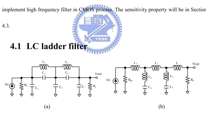
4.1 LC ladder filter
(a) (b)
Figure 4.1 the 5th elliptic LC ladder
There are two possible topologies to implement the 5th order elliptic filter by LC ladder
structure. The zeros are generated by the LC tanks at their resonant frequencies. One LC tank
off the input-output path at the tank’s resonant frequency. On the other hand, the serial LC
tank forms a ”short circuit” at resonant frequency (zeros) as shown in Figure 4.1. The parallel
LC tank topology is preferred owing to less inductor, therefore less gyrators are used. There
are four Gms for a gyrator, so Figure 4.1(b) is power wasting topology. Moreover, serial LC
tank topology does not have desired capacitance to ground in all the nodes and will distort
frequency response. If the LC tank is lossless, there will be a very high Q zero. In the CMOS
process, the on-chip inductors have serious parasitic effect and the resistance variation is
serious. The LC ladder can’t be implemented by simply putting some RLC components,
especially when the circuit is used for high frequency application. The LC ladder filter has
good sensitivity property. In previous chapter, the transconductor is introduced in the form of
inductors or resistances. The detail transfer function of 5th elliptic LC ladder filter is analyzed
in Appendix A.
4.2 LC Gm-C filter
As mentioned above, the variation of on-chip resistors is critical. And passive inductor
has parasitic resistance which can’t achieve a high Q and high frequency zeros in the CMOS
process. Since these restrictions are serious, the passive element must be replaced by analog
circuits. Although circuits need power to boost and have worse linearity, there are many
Figure 4.2 Differential Gm connected as resistance
Figure 4.3 Differential Gm connected as inductance by gyrator approach
The Gm block has non-ideal effects which are finite output impedance and RHP-zero.
When Gm is connected as passive element, it will add parasitic components as shown in
Figure 4.4 and 4.5. In order to reduce go and increase τ, the Gm should be design by a simple
structure with some circuit to increase Rout.
(a) (b)
Figure 4.5 Inductor implemented by non-ideal Gm with finite (a) Rout (b) RHP-zero
The gyrator using integrator has -90o phase shift, but in chapter 3 the integrator shows
very poor behavior at low and high frequency. That is, the phase of the integrator is very far
from being -90o for frequency f <<fint3db and f >>fRHP_zero. We can analyze simple gyrator
shown in Figure 4.6. From (4.1) we can draw Rin V.S. frequency plot. The curve has two
corners which point to Gm fint3db and fGmBW, respectively. When signal frequency is low (f
<<fint3db), the gyrator acts as resistor with the value depends on Rout of the Gm. Even at DC
frequency, the resistor only causes little loss without changing response. But when signal
frequency is high (f >>fRHP_zero ), it does not matter whether the phase of the integrator is still
-90 o or not : the capacitors connected to the filter nodes will short circuit them because their
typical attenuation of the signal at high frequencies. 2 m o
g
g
C
g
oτ
1
Figure 4.6 Non-ideal Gm effects the inductor
Another question will rise if the Gm output impedance is too “negative” and the Gm will
have the right-half-plane zero. For a stand-alone integrator, it could become unstable. Even so,
a gyrator built with Gm blocks will remain stable. This is owing to the feedback loops
inherent to a filter constructed with gyrators as shown in Figure 4.7. It can be found that
gyrator based inductor input impedance Rin is negative at zero frequency. But when the
inductor lies in LC ladder filter, the filter response at DC will be stable due to the input/output
impedance of the filter shown in Figure 4.8. That is the Gm could be designed at negative
output impedance which is not too far from zero.
(4.1) ) 1 ( )] 1 ( [ ] 1 ) 1 ( [ 2 2
τ
τ
τ
s gm go sC Ix Vx Rin Ix s gm go sC s gm Vx − + = = − = − − × + × − ×gm*
(1-s )
C
-1/go
-1/go
Vx
Ix
-gm*
(1-s )
Figure 4.7 Negative impedance at DC frequency
Figure 4.8 LC ladder low frequency gain with negative impedance
After element replacement, the filter has changed from Figure 4.1 to Figure 4.9. Input
current source is made by Gm for its high input resistance. Grounded resistance is replaced by
circuit shown in Figure 4.2. The floating inductor is made of at least four Gm. The circuit has
to connect output buffer in order to load high capacitance measure equipment. The simple
common source follower can be used as a buffer design for its excellent frequency response.
0
)
(
)
(
)
0
(
>
+
−
+
−
+
=
L b a S LR
R
R
R
R
H
Figure 4.9 the 5th elliptic ladder filter using Gm-C technique
The internal nodes gain may be a serious problem since it could be higher than output
gain. And for UWB receiver, the filter is the last element in receiver path. The filter input
swing is very large. If the internal node swing is higher than output swing, the Gm blocks
may saturate and reduce dynamic range. The reason of internal node peaking is that it is band
pass transform function in Figure 4.10(b). The analysis is assumed using 3rd elliptic Gm-C
filter with ideal Gm and filter has the same input/output impedance. Since the most serious
internal node peaking comes from the two capacitors of gyrator circuits, there must have some
adjustment. In Figure 4.10 (a), the X & Y are defined by the connection with internal
capacitor. The output of X and the input of Y connect with the internal capacitor. For a
desired inductor value with minimum power and acceptable process variation, the internal
capacitor can be chosen as 0.4pf. Then the product of X and Y is known as 4gm2 and the gm
is the transconductance of unit Gm since this can relax the design complexity and variation.
Figure 4.10(b) is the internal nodes magnitude response when X = Y = 2gm. We can see Vb
Y. Consider all the information, the X/Y ratio can be found as 1/4 in Figure 4.10(c). After
adjustment, the result can be shown in Figure 4.11 and we can see all the internal response is
less than one except a little higher in the pass band edge.
(a) (b)
(c)
Figure 4.10 Adjust gm value in gyrator
100 200 0 300 0.5 1.0 1.5 2.0 0.0 2.5 Frequency In te rn a l n o d e G a in X Y
X:Y=1:4
power
Assume
g
m∝
=
+
>
=
=
∗
min
output)
Gain vs
internal
(Max
3
0.4pF)
Cap
(For
4
2Y
X
X
Y
g
Y
X
m 100 200 0 300 0.2 0.4 0.6 0.8 1.0 1.2 0.0 1.4 Frequency In te rn a l n o d e G a in 0.4 1.2 Vb Va Va VbThe LC ladder can also change to equal-ripple filter in Figure 4.12. The filter has higher
cutoff frequency than elliptic filter since the filter does not need high frequency zeros. The
magnitude response will be compared in section 4.4.
Figure 4.12 the 5th equal-ripple LC ladder filter using Gm-C technique
4.3 Sensitivity
We have to be concerned with a problem: components with exact design will generally
not be available. Maybe there are just desired components with exact value in the laboratory,
but it’s generally impossible or too expensive in CMOS process. So the sensitivity has to be
analyzed especially when designing high frequency filter with high quality factor.
The definition of sensitivity of equation T with respect to x:
)
u
du
u)
d(ln
(for
ln
ln
/
/
=
∂
∂
=
∂
∂
=
∂
∂
=
x
T
x
T
T
x
x
x
T
T
S
xT (4.2)Sensitivity is the ratio of the relative error of the function T(s) to the relative
From 5th order elliptic transfer function of (2.1):
)
)(
)(
)(
)(
(
)
)(
)(
)(
(
)
)(
(
)
(
)
(
)
(
5 4 3 2 1 4 3 2 1 0 1 1 2 2 3 3 4 4 5 1 2 0 2p
s
p
s
p
s
p
s
p
s
z
s
z
s
z
s
z
s
A
s
s
s
s
s
s
s
A
s
D
s
N
s
T
−
−
−
−
−
−
−
−
−
=
+
+
+
+
+
+
+
=
=
β
β
β
β
β
α
α
(4.3)where A is constant and z1&z2, z3&z4, p2&p3, p4&p5 are conjugate.
To calculate the sensitivities to an element x by using (4.2) and (4.3):
{
}
... [ ] ... [ ] ... [ ] ... [ )] ln( ... ) [ln( )] ln( ... ) [ln( ln ) ( ln ln ) ( ln ln ) ) ( ) ( ln( ln ) ( ln 5 5 1 1 4 4 1 1 5 5 1 1 4 4 1 1 5 1 4 1 ) ( 5 1 4 1 p s S p p s S p z s S z z s S z S p s x p x p s x p x z s x z x z s x z x S p s p s z s z s x x S x s D x s N x s D s N x s T S p x p x z x z x A x A x A x s T x − + + − + − + + − − = −∂ ∂ + + −∂ ∂ + −∂ ∂ + + −∂ ∂ − = − + + − − − + + − ∂ ∂ + = ∂ ∂ − ∂ ∂ = ∂ ∂ = ∂ ∂ = (4.4)The deriving function is assumed all zeros and poles are functions of the component x of
concern. If any zi or pi is independent of x, the corresponding sensitivity term is set to zero.
(4.4) can be observed that the sensitivity becomes large near all the zeros and all the poles.
For low pass filter the transfer function zeros are normally in the stop band, so it needs to be
less concerned with the zeros. The filter DC gain is constant, so the sensitivity is always zero.
By neglecting all remaining terms:
5 1 ) ( 5 1