國立交通大學
電子物理學系
碩士論文
摻雜不同濃度的硼在金屬誘發結晶前
對矽奈米晶 SONOS 記憶體的影響
Impacts of Boron Doping on MILC Growth of
Si-NCs SONOS Memory and Device Property
指導教授 : 趙天生博士
研究生 : 張芳瑜
2
摻雜不同濃度的硼在金屬誘發結晶前
對矽奈米晶 SONOS 記憶體的影響
Impacts of Boron Doping on MILC Growth of Si-NCs
SONOS Memory and Device Property
研究生: 張芳瑜 Student: Fang Yu Chang
指導教授: 趙天生 Advisor: Tien Sheng Chao
國立交通大學 電子物理學系
碩士論文
A Thesis
Submitted to Department of Electrophysics
National Chiao Tung University
In Partial Fulfillment of the Requirements
for the Degree of Master of Science
In Electrophysics
July 2013
Hsinchu, Taiwan, Republic of China
i
摻雜不同濃度的硼在金屬誘發結晶前
對矽奈米晶 SONOS 記憶體的影響
研究生:張芳瑜 指導教授:趙天生 博
士國立交通大學
電子物理研究所碩士班
摘要
金屬誘發側向結晶的技術是利用金屬可在低溫下控制結晶的位
置使非晶矽重新結晶為多晶矽。Hayzelden 在 1992 年發現鎳金屬具
有兩個優點。一個是快速遷移的特性;另一個是鎳的矽化物和結晶的
矽有較小的晶格常數誤差。因此金屬誘發側向結晶中的金屬常常使用
鎳。為了得到更大的結晶的晶粒,使晶格缺陷減少並讓載子可以更快
速的移動,許多方法針對加大結晶晶粒做研究。在金屬誘發側向結晶
前摻雜硼是否能幫助鎳金屬更快速的遷移至今仍是一個具爭議性的
議題。支持的團隊認為硼可以降低鎳的矽化物形成的能量並修補結晶
矽和鎳的矽化物 0.4%的晶格常數誤差,因而可加快鎳及其矽化物遷
移,使得結晶更有效率且得到較大的結晶晶粒。然而,反對的團隊認
為在金屬誘發側向結晶前摻雜硼,硼會是一個干擾因子會阻礙鎳金屬
側向遷移,導致結晶速率緩慢以及晶粒變小。
我們好奇硼是否真的能幫助金屬鎳結晶。因此在 SONOS 記憶體的
ii
通道中應用金屬誘發側向結晶的技術,並在結晶前摻雜不同濃度的硼
(5 ∗ 10
14𝑐𝑚
−2, 1 ∗ 10
15𝑐𝑚
−2) 做比較。這兩組樣本,我們會分別從
物性以及電性做討論,包括 XRD 分析、電導值、載子寫入和抹除速
度、漏電流比較、源極和集極電阻值量測、可靠度探討。
在此研究中我們證實在 SONOS 記憶體通道中先摻雜硼會幫助鎳
擴散,使結晶的晶粒更大。摻雜硼濃度1 ∗ 10
15𝑐𝑚
−2的樣本金屬側向
結晶長度為摻雜硼濃度5 ∗ 10
14𝑐𝑚
−2的兩倍;對比 T. Ma 發現當摻雜
濃度為3 ∗ 10
15𝑐𝑚
−2時金屬側向結晶長度為濃度3 ∗ 10
14𝑐𝑚
−2的兩倍
的結果,在 SONOS 記憶體中我們可將硼的濃度下修正至1 ∗ 10
15𝑐𝑚
−2。
此外,摻雜硼濃度較高的樣品具有較大的晶粒、不同尺寸下有較小的
變異性、較高的載子遷移率、較快的寫入和抹除速度、較低的源極和
集極電阻值,較長的資料保存時間。本論文中我們將逐步的檢驗並驗
證硼幫助鎳擴散的現象,且證實此現象會提升 SONOS 記憶體物性以及
電性的性質。
iii
Impacts of Boron Doping on MILC Growth of Si-NCs SONOS Memory
and Device Property
Student: Fang-Yu Chang Advisor: Dr. Tien-Sheng Chao
Institute of Electrophysics
National Chiao Tung University
Abstract
Metal Induced Lateral Crystallization (MILC) technique has been purposed due to metal can be used to cause crystallization at controlled locations with low temperature. In 1992 Hayzelden et al. found that using nickel in MILC process showed two advantages. One is fast migration property. The other is small lattice constant mismatch between NiSi2 and crystal silicon (c-Si). So nickel is common used as MILC source in experiments now. Large crystal grain size can reduce defects and enhance carriers mobility, many research focus on how to increase grain size. Would boron enhance nickel crystallization when boron doping before MILC process is a controversial issue. The support groups think boron can reduce NiSi2 formation energy and modify lattice constant mismatch between crystal silicon and NiSi2 resulting in NiSi2 faster migration, longer metal induced lateral crystallization (MILC) length and larger grain size. However, the opposite groups think boron atoms are interrupt factor for crystallization. They believe doping boron with MILC process would block nickel crystallization causing short MILC length and small grain size. Weather boron enhance or reduce nickel diffusion is what we curious. So the experiments are designed by different boron doping concentration (5 ∗ 1014𝑐𝑚−2, 1 ∗ 1015𝑐𝑚−2) samples with MILC crystallization on SONOS memories. We discuss this effect in physical and electrical parts, including XRD analysis, conductance
iv
measurement, program/erase speed, source/drain resistance extraction, GIDL current, retention and endurance researches.
The boron enhanced nickel diffusion effect is successfully proved in SONOS memories. We also found with double difference of boron doping concentration (5 ∗ 1014𝑐𝑚−2, 1 ∗ 1015𝑐𝑚−2) leading to double difference of grain size. Therefore, T. Ma et al. found MILC length double increase effect between boron dosages 3 ∗ 1014𝑐𝑚−2 and 3 ∗ 1015𝑐𝑚−2 can be modified to 1 ∗ 1015𝑐𝑚−2 in SONOS memories. In addition, the high boron doping device shows better performance presenting large grain size, small variation, high mobility, fast program/erase speed, low resistance and long retention time. In this thesis, we gradually examine and verify boron enhanced nickel diffusion phenomenon which can promote SONOS memories physical and electrical characteristics.
v
誌謝
感謝交大栽培我六年,讓我學習各種知識與技能,結交許多好朋友,
非常珍惜在這裡認識的每一個人以及感謝所遇到的每一件事,能在交
大成長與畢業是一輩子引以為傲的事。
首先感謝我的父親張博信先生與母親詹素華女士的支持與鼓勵,讓我
能安心、順利的完成學業。在碩班期間,有時候比較忙所以較少回家,
很謝謝你們總是把家裡的一切都照顧的那麼好,使我每次回家都有幸
福無比的感覺。
特別感謝趙天生老師讓我進入實驗室,讓我有機會和大家一起學習半
導體物理製成的原理與技術。謝謝老師耐心的指導我們,關心大家的
學習狀況與身體健康。也非常謝謝您幫我找工作,寫推薦信,告訴我
人生規劃與方向,並在我遇到實驗瓶頸時,提供我寶貴的意見。此外,
也謝謝師母會來實驗室和大家聊天,幫忙我們排解壓力;尾牙時讓大
家去老師家玩,讓大家都留下甜美的回憶。
謝謝廖家駿學長和嚴立丞學長的指導讓我能順利完成碩班的研究。很
感謝廖家駿學長在繁忙工作下仍每星期五抽空來幫儀儒和我 meeting,
並耐心的告訴我們實驗方向與建議,安排我們的實驗進度,幫我們在
工作面試前做模擬面試,改好幾次論文內容,還自掏腰包請我們吃飯,
非常感謝你的照顧。謝謝嚴立丞學長教我做人的道理,帶我進 NDL 做
vi
實驗,給予我實驗上的幫助,幫忙我改論文,謝謝你的幫忙。也很感
激教我取R
SD阻值的蘇彬老師,擔任我的口委還細心幫我改論文的許
鉦宗老師和多花三倍時間幫我打 XRD 的姚潔宜工程師。
此外,也非常感謝大學時數學系的導師林琦焜老師,在我來電物
所後仍很關心與照顧我。並謝謝電物羅志偉老師,許世英老師,趙如
蘋老師大學時超有耐心的教導,讓我能有能力與機會到電物所就讀。
超級感謝湯乾紹學長在我找工作時大力的幫忙,還帶著佳玉學姊
一起來學校指導和關心我,真的很謝謝你們。謝謝劉邵軒學長幫我補
強許多半導體物理的概念,且主動關心學弟妹們的實驗進度並指導我
們。謝謝吳翊鴻學長指導我,且去工作後還會回來給我寶貴的意見和
方向。謝謝吳立盈學姊、林岷臻學姊在我剛進實驗室時的指導與照顧。
謝謝呂侑倫學長,總是把歡笑帶回實驗室,讓我們歡樂的度過碩班的
日子。謝謝江宗育學長留下貨給我量,讓我在測試片做不出來時有換
題目的選擇並能順利畢業。謝謝陳昱璇學姊把實驗室照顧的無微不至,
讓每天去實驗室都有回家的感覺。還謝謝林哲緯學長,呂宜憲學長常
常請學弟妹吃東西,讓我們覺得超有口福的。謝謝張添舜學長、卓大
鈞學長、林哲毅學長、唐明慈學姊和郭柔含學姊,對學弟妹實驗上的
指導與幫助。謝謝李時璟學長,王冠迪學長,葉啟瑞學長畢業後還抽
空回來和大家一起出去玩。也超感謝碩二的夥伴們陳儀儒,王貽泓,
vii
解偉斌,楊卓利的扶持和鼓勵,很開心看到大家都能順利的畢業。謝
謝可愛學弟妹黃品烝,鄭芳晴,方柏崴,林可立的陪伴,讓我們快樂
的度過碩二這一年。能從這間實驗室畢業真的很幸運,感謝所有學長
姐無私的付出,同學們的鼓勵,學弟妹的陪伴。畢業後一定會永遠記
得大家,由衷感謝在交大六年來幫助我的每一個人,也期許自己在未
來的日子能幫助許多的人,回饋社會。
張芳瑜 誌於 最感謝的交通大學
viii
Contents
Abstract (Chinese) ...
iAbstract (English) ... iii
Acknowledgement (Chinese) ...
vContents ...
viiiTable Caption ...
xiFigure Caption ...
xiiChapter 1
Introduction
1.1 General Background
1.1.1 Thin-Film Transistors ... 11.1.2 SONOS Memory ... 2
1.1.3 Bottom Gate and Top Gate Devices ... 3
1.2 Silicon Nano-Crystal (Si-NCs) Technology
... 31.3 Metal Induced Lateral Crystallization (MILC) Technology
... 41.4 Dopant Activation
... 51.5 Motivation
... 61.6 The Purpose and Value of This Thesis
... 71.7 Organization of This Thesis
... 7Chapter 2
Device Fabrication and Experimental Setup
2.1 Overview
... 15ix
2.3 Measurement and Equipment Setup
... 162.4 Operation and Parameter Extraction of TFT-SONOS Memory
2.4.1 Threshold Voltage ... 17 2.4.2 Subthreshold Swing ... 17 2.4.3 Source/Drain Resistance... 18 2.4.4 Fowler-Nordheim (FN) Mechanism ... 18 2.4.5 Pelgrom Plot ... 19 2.4.6 Arrhenius Plot ... 192.5 Characteristic of Memory
2.5.1 Characteristic of Retention ... 20 2.5.2 Characteristic of Endurance ... 20Chapter 3
Characteristics of Si-NCs-SONOS Nonvolatile Memory
3.1 Overview
... 283.2 Source/Drain Doping Dependence
3.2.1 X-ray Diffraction (XRD) Analysis ... 293.2.2 Transistor Performance ... 29
3.2.3 Program/Erase Characteristics ... 31
3.2.4 The Reverse Read and Forward Read ... 32
3.2.5 The Comparison of Source/Drain Resistance and Overlap Length ... 32
3.2.6 The Comparison of Off-Leakage ... 34
3.2.7 The Comparison of Retention Characteristics ... 35
3.2.8 The Comparison of Endurance Characteristics ... 37
x
Chapter 4
Conclusion and Future Work
4.1 Conclusion
... 614.2 Future Work
... 62Reference
... 63xi
Table Caption
Chapter 1
Table 1.1 Table 1.1. Technology trends in ITRS 2012………...
21
Table 1.2 Table 2.2 Summary of Metal Induced Crystallization (MILC)
observations……… 21
Chapter 2
Table 2.1 Table 2.1. JOE E. Brewer reported the value and mechanism
relation in 2007………... 33
Chapter 3
Table 3.1 Table 3.1. The Si-NCs-SONOS memories characteristics were presented with MILC crystallization process……… 39 Table 3.2 The slope, universal mobility, source/drain resistance and overlap
length for high and low boron doping devices……… 39 Table 3.3 The of window losses in 0.05V and 0.1V are about 0.496eV,
0.545eV for boron doping concentration 5 ∗ 1014𝑐𝑚−2 and 0.704eV, 0.709eV for boron doping concentration 1 ∗ 1015𝑐𝑚−2………... 40 Table 3.4 Both high and low doping devices values approximate 0.6eV
which charge loss mechanism are dominated by oxide defects…… 40 Table 3.5 The XRD result of boron doping concentrtion 5 ∗ 1014𝑐𝑚−2 and
xii
Figure Caption
Chapter 1
Fig 1.1 The top graph is TFT array and color filter substrates which are made into an LCD panel by assembling then with a sealant; the bottom graph is the flowchart of making an amorphous silicon TFT array using a bottom gate TFT structure and an independent storage
capacitor………. 22
Fig. 1.2 Plan-view EBSD map color-coded with the IPF coloring in the SPC sample normal direction . The grain boundaries are highlighted with black lines and twins are highlighted with white lines……… 23
Fig 1.3 The structure of (a) floating gate and (b) SONOS devices……… 24
Fig 1.4 The structure of (a) top gate and (b) bottom gate devices……… 25
Fig. 1.5 A schematic illustration of the MILC reaction model………... 26
Chapter 2
Fig. 2.1 Thermal oxide was grown on silicon wafer, depositing 150nm amorphous silicon and annealed to poly-silicon……… 33Fig. 2.2. Gate was defined and implanted boron with 5 ∗ 1015𝑐𝑚−2 dosage… 34 Fig. 2.3. Blocking oxide was deposited and used in-situ technique to embed Si-NCs in nitride film, as shown in fig. 2.2………... 34
Fig. 2.4 Tunneling oxide was deposited……….. 35
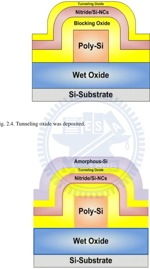
Fig. 2.5 Amorphous silicon was deposited which made as device channel…… 35
Fig. 2.6 Active region was defined and implanted with different boron dosage. (1 ∗ 10𝟏𝟓𝑐𝑚−𝟐, 5 ∗ 10𝟏𝟒𝑐𝑚−𝟐)……… 36 Fig. 2.7 Using MILC technique at 520 ℃ , amorphous silicon was
xiii
recrystallized to poly-silicon………. 36 Fig. 2.8 The schematic diagram shows gas flow of in-situ deposition of
Si-NCs in nitride……… 37
Fig. 2.9 The experimental setup for the transfer characteristic and program/erase characteristic of SONOS with Si nanocrystals
memory……….. 37
Fig. 2.10 A schematic of the FN tunneling during programming (left) and erasing (right) in the electric field……….... 38 Fig. 2.11 Different oxide thickness present in Pelgrom plot. If 𝐴𝑣𝑡= 3.8, then
7nm oxide thickness will have about 400mV variation in threshold voltage. If we want to variation smaller than 100mV, than 𝐴𝑣𝑡value should be choose smaller than one……… 38
Chapter 3
Fig. 3.1 Fig. 3.2 Fig. 3.3
The AFM graph of Si-NCs deposited on Si3N4 layer……….. The TEM graph of Si-NCs deposited on Si3N4 layer……….. X-ray diffraction (XRD) results of poly-silicon channel with different boron doping concentrations………...
41 42
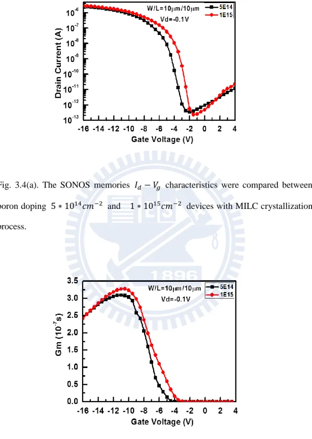
42 Fig. 3.4 (a) The SONOS memories 𝐼𝑑− 𝑉𝑔 characteristics were compared
between boron doping 5 ∗ 1014𝑐𝑚−2 and 1 ∗ 1015𝑐𝑚−2 devices with MILC crystallization process. (b) The 𝐺𝑚 is higher in doping
1 ∗ 1015𝑐𝑚−2 device……… 43
Fig. 3.5 The pelgrom plot shows devices variation. The high boron doping with slop 0.57 V/μm is smaller than low boron doping slop
1.1 V/μm……… 44
xiv
boron doping devices. The high boron doping device shows better
subthreshold leakage suppression as channel length beyond μm….. 44 Fig. 3.7 (a) The memory window are 0.48, 1.31V and 1.84V as programming
voltage 18V, 20V and 22V in boron doping 5 ∗ 1014𝑐𝑚−2 device. (b) The memory window are 0.5, 1.6V and 2V as programming voltage 18V, 20V and 22V in boron doping 1 ∗ 1015𝑐𝑚−2 device…. 45 Fig. 3.8 (a) The memory window are 0.12 and 1.26V as erasing voltage 18V
and 20V in boron doping 5 ∗ 1014𝑐𝑚−2 device. (b) The memory window are 1.1 and 2V as erasing voltage 18V and 20V in boron doping 1 ∗ 1015𝑐𝑚−2 device………... 46 Fig. 3.9
Fig. 3.10
(a) The programming speed curves show threshold voltage values ranging from 18V to 22V with filled and open symbols presenting low and high boron doping devices respectively. (b) The erasing speed curves show threshold voltage values ranging from -18V to -20V with filled and open symbols presenting low and high boron doping devices respectively. ………. The schematic of channel conduct in bottom gate device……….
47 48 Fig. 3.11 (a) The 𝐼𝑑− 𝑉𝑔 curves of initial state, programmed state, forward
read and reverse read in boron doping 5 ∗ 1014𝑐𝑚−2 device. (b) The 𝐼𝑑 − 𝑉𝑔 curves of initial state, programmed state, forward read and
reverse read in boron doping 1 ∗ 1015𝑐𝑚−2 device……… 49 Fig. 3.12 The 𝑅𝑆𝐷 and ∆L are gate bias dependent which decrease as V𝑔
increasing……… 49
Fig. 3.13 The La Moneda method extracting RSD and ∆L procedures involve three plotting which are discussed on channel length 1μm, 5μm and
xv
10μm devices. The first procedure is generating the plots of 𝑹𝒎 verse (𝑉𝐺𝑆 − 𝑉𝑡)−1. The boron dosage (a) 5 ∗ 1014𝑐𝑚−2 and (b)
1 ∗ 1015𝑐𝑚−2 devices.……….. 50
Fig. 3.14 The second procedure is differential of Rm and m, so we can get RSD values. The boron dosage (a) 5 ∗ 1014𝑐𝑚−2 and (b) 1 ∗
1015𝑐𝑚−2 devices.……… 51
Fig. 3.15 The final procedure is differential the m and L, the intercept point on x-axis is overlap length. The boron dosage (a) 5 ∗ 1014𝑐𝑚−2 and (b) 1 ∗ 1015𝑐𝑚−2 devices.………... 52 Fig. 3.16 Higher doping concentration device has bigger grain size and fewer
scattering than lower boron concentration device leading to large
mobility value………. 53
Fig. 3.17 The top graph is energy band diagram for PMOS device. The bottom graph is electric field versus distance between 𝑆𝑖/𝑆𝑖𝑂2 interface and drain [3.11]. The tunneling distance 𝑥𝑡𝑢𝑛 is much less than the total
depletion length……….. 54
Fig. 3.18 The electrons tunneling from the valence band subsequently leave via the substrate and the generated holes enter the drain creating the
leakage current………... 54
Fig. 3.19 The boron doping (a) 5 ∗ 1014𝑐𝑚−2 and (b) 1 ∗ 1015𝑐𝑚−2 devices shows source and drain sides GIDL current. The filled simples are current from drain to gate and the open simples are current from
source to gate. 55
Fig. 3.20 The average GIDL current for source and drain sides of two different boron doping (5 ∗ 1014𝑐𝑚−2, 1 ∗ 1015𝑐𝑚−2) concentration before
xvi
MILC process samples and one MILC process before boron doping 5 ∗ 1015𝑐𝑚−2 concentration sample, respectively……… 56 Fig. 3.21 T. Ma and M. Wing have reported MILC rate is found to increase at
the highest dose of 3 ∗ 1015𝑐𝑚−2………. 56 Fig. 3.22 The high and low doping devices have small charge loss percentages
of 3.5% and 3.3% as time of stress increasing to 104 seconds………... 57 Fig. 3.23 The high and low boron doping devices have similar trends as
constant temperature before 102 seconds and the loss percentages increase to 24% and 23.3% as 104 seconds……… 57 Fig. 3.24 For temperature at 125℃, the high and low doping devices charge
loss values are 44.3% and 62.6% at 104 seconds………... 58 Fig. 3.25 The Arrhenius plots of retention time characteristics for window
dropping 0.05V and 0.1V………... 58
Fig. 3.26 The device were programmed at 20V for 0.8s and erased at -20V for 1.6s. A large dropping in programmed threshold voltage and a slightly decrease in erased threshold voltage are observed in both (a) high and (b) low doping devices after 103 P/E cycles……….. 59 Fig. 3.27 The ∆S. S. and ∆𝑉𝑡ℎ versus the cycling numbers graphs.
Meanwhile, ∆S. S. shows a similar trend to ∆𝑉𝑡ℎ with an approximate relation of (a) ∆S. S.∗ 10~∆𝑉𝑡ℎ and (b) ∆S. S.∗ 2~∆𝑉𝑡ℎ for high and low boron doping device……… 60
1
Chapter 1
Introduction
1.1 General Background
1.1.1 Thin-Film Transistors
Thin film transistor is one of field effect transistors. The roughly production methods are depositing different thin films on substrate, such as semiconductor active layers, dielectric layers and metal electrode layers. Recently, amorphous silicon (α-Si) thin film transistors (TFTs) are very potential technique for the application of active matrix liquid crystal devices (AM-LCDs), active matrix organic light-emitting diodes (AM-OLEDs) and active matrix flat panel displays (AM-FPDs) as shown in Fig. 1.1[1.1]. However, α-Si films have slower carrier transportation rate due to small grain size and many grain boundaries. In addition, the rapid thermal process and low thermal budget are needed for high performance device. Therefore, polycrystalline silicon (poly-Si) thin film transistors have been proposed to replace α-Si. Poly-Si show several advantages than α-Si, including low cost, simple fabrication process, good electrical properties and integrated peripheral driver circuits fabricated on glass substrates achieving system on panel (SOP) and 3-D circuits [1.2-1.4].
Poly-Si can be prepared by direct deposition onto a substrate or by crystallization of α-Si precursor. The poly-Si prepared by direct deposition exhibits a columnar structure and small grains. As a result, it electrical properties are poor and decrease mobility, typically about 5cm2/𝑉 ∙ 𝑠 [1.5]. There are many different approaches to crystallize α-Si to poly-Si TFTs, including Solid Phase Crystallization (SPC), Excimer Laser Annealing (ELA), Metal Induced Crystallization (MIC) and so on. However, SPC require high temperature annealing and crystallize in random directions resulting
2
in small grain size and high level impurities as shown in Fig. 1.2 [1.6-1.7]. ELA crystallization show better quality but high cost [1.8]. MIC crystallization show large grain size comparing to SPC and with low cost comparing to ELA. But it has metal contamination disadvantage [1.9]. Therefore, Metal Induced Lateral Crystallization (MILC) technique has been developed to overcome above problems.
1.1.2 SONOS Memory
Due to escalating use of computer, personal notebook, mobile capabilities and electronic portable equipment nonvolatile semiconductor memory (NVSM) are increasingly high demand. The floating gate (FG) non-volatile memory was invented by S.M. Sze and Dawon Kahang in April 1967 with five layers, including control gate, blocking oxide, floating gate, tunneling oxide and semiconductor, as shown in Fig. 1.3(a) [1.10]. The electron trapped inside floating gate creates a built-in electric field that provides an electric force leading to electrons tunneling back to channel. According to research, tunneling oxide thinner than 4nm can perfect avoid point defects trapping tunneling electrons. In fact, fabricating free defect oxide is impossible. In addition, Probability of Frenkel-Poole emission and direct tunneling occurrence increase as tunneling oxide thickness decreasing. Therefore, floating gate memories require tunneling oxide thickness about 8nm to 11nm resulting in big scaling down hinders beyond 40nm node technology as shown in Table 1.1 [1.11-1.13]. The SONOS type memory which replaced floating gate layer by nitride with discrete traps has been proposed. The electrons are stored in silicon nitride between blocking oxide and tunneling oxide as shown Fig. 1.3(b). The thinner tunneling oxide of SONOS memory can be achieved due to discrete trapping states [1.14-1.17]. Thus, SONOS type memories present longer retention time lower voltage
3
operation faster program/erase speed and compatible to CMOS technology. It has high potential in NVSM market.
1.1.3 Bottom Gate and Top Gate Devices
As far as to now, enhancing field effect mobility, decreasing process temperature and developing strategies to reduce the carrier density in the channel are important issues. Changing devices structure is one of common ways. Many papers have compared the difference between top gate and bottom gate devices, as shown in Fig. 1.4 [1.9]. The performance characteristic of the top-gate and the bottom gate TFTs are quite different. The critical channel region in the top-gate TFTs is the surface layer of the Si film which causes significant surface roughness due to large lateral grain growth. This phenomenon results in diminished and non-uniform device performance for the top-gate TFTs [1.18].
For bottom gate devices, the main challenge is cannot self-alignment. So the application of bottom gate device is seriously limited. However, there are many methods have been proposed by performing lithography through the backside of a transparent substrate to solve this problem. The lithography independent self-alignment bottom gate TFT (SABG-TFT) technology is also been reported and experimentally demonstrated [1.18]. Besides, bottom gate devices have higher circuit density and better topography than top gate devices, it still has a great potential.
1.2 Silicon NanoCrystal (Si-NCs) Technology
The metal-oxide-semiconductor (MOS) memory structures based on nanocrystals (NCs) have exhibited faster programming and erasing speed, simple fabrication process and great retention, thus attracting much research attention. The Si-NCs can
4
be formed in Si-rich SiN𝑥 layers using different chemical vapor deposition (CVD) techniques or by low energy silicon implantation technique. The reliability of nanocrystal memories depends on their thermal properties, work function, average size, and density. Electrons are trapped inside nanocrystals which isolate to others and stable confine in the well creating by the trapping layer and nanocrystals work function difference. Recently, the Si, Ge, high-k dielectric, metal, silicide and metal oxide are used for storage node application in the NCs non-volatile memory device. The NCs memory devices can fabricate the thinner tunneling oxide due to discrete trapped states. On the other hand, the deep trapped level states of nanocrystals could future promote data retention [1.19].
Chiang et al. [1.20] invented in situ embedded silicon nanocrystals in silicon nitride method and found 30s SiCl2H2 deposition having maximum trapping cross areas (product of dot size and dot density). We used this method on bottom gate TFT-SONOS memory and characterized it electrical properties.
1.3 Metal Induced Lateral Crystallization (MILC) Technology
Poly-Si deposition usually occurs at high temperature (≥ 550℃) and unwanted nucleation is kept at a maximum during crystal growth resulting in rough films. Fortunately, for silicon, the nucleation activation energy is higher than the crystallization energy. In other words, a high temperature is needed to form nuclei while a lower temperature is sufficient to cause their growth into a crystal. So keeping a low number of nuclei during a low temperature anneal allows crystal growth but suppresses additional homogeneous nucleation and nucleation at the α-Si substrate interface. External agents like metal or Germanium can be used to cause nucleation at controlled locations using low temperature.
5
In MIC of α-Si, certain metals are used to lower the crystallization temperature. A summary of various MIC experiments is given in Table 1.2. In 1992, Hayzelden et al. [1.6] formed NiSi2 by a Ni implant and 400℃ anneal. Upon further annealing of films at 500℃, they observed a silicide mediated phase transformation of α-Si to crystalline silicon (c-Si). This lateral crystallization is mediated by the silicide formed in the MIC region. NiSi2 precipitates migrated through the α-Si leaving a trail of c-Si and growth occurred parallel to the <111> direction. Hence, MILC is called a catalytic phase transformation, and poly crystals formed via MILC are free from metal contamination. When Ni is used as a catalyst for MILC, the growth rate are about 5 𝑚
⁄ at a temperature of 550℃ and 2 𝑚 ⁄ at 500℃ [1.9]. The crystallization obtained by this method presenting long growth length along unidirectional. This was the first observation of MILC [1.21].
The schematic diagram of MILC mechanism is shown in Fig. 1.5 [1.22]. The needle-like crystal growth during MILC utilizes the lateral migration of metals to enhance the grain size. This method is able to produce poly-Si thin film largely under a low temperature about 500℃, free of metal contamination and low cost; therefore, good quality poly-Si is available and highly efficient poly-Si TFT can also be produced [1.21].
1.4 Dopant Activation
Dopant activation is the process of getting the desired electronic contribution from impurity species in a semiconductor host which is crucial way for obtaining high performance transistors [1.23]. The way is often applied on thermal energy following the ion implantation of dopants. As thermal annealing, the vacancies generate at elevated temperature facilitate the movement of dopants from interstitial to
6
substitutional lattice site while damage from implantation process recrystallizes. The mechanism of dopant activation can be related to rearrangement of silicon and dopant atoms which can get large grains and better devices performance.
1.5 Motivation
The image transport speed, brightness, resolution and 3-DIC performance are significant dependent on the carrier mobility of TFTs which means dependent on the crystallization (grain size) on silicon substrate. Generally, amorphous silicon (α-Si) TFTs have an electron mobility of around 0.5𝑐𝑚2/V∙sec. However, the electron mobility value can be increased up to more than 200𝑐𝑚2/V∙sec when the α-Si is crystallized into poly-Si [1.24]. In addition, poly-Si TFTs usually have defects at the grain boundaries in the channel region, which leads to degradation in device performance. This includes high threshold voltage, low mobility and high leakage current. It is believed that the electrical properties of the TFTs can be improved if the grain size of the poly-silicon can be enhanced and the number of grain boundaries in the channel region can be minimizes [1.25].
In addition, series resistance in transistors and contact resistivity increasing due to continued shrinking is the hurdles in improving drive current. Dopant activation technique is applied to decrease sheet resistance. The interesting application of silicon Nano-crystals, dopant activation and MILC techniques in TFT-SONOS memory is demonstrated and its effects on the reliability are analyzed in this thesis.
7
1.6 The Purpose and Value of This Thesis
The past experiment has shown that MILC rate and the crystallization quality are sensitive to the doping type and concentration. Doping with phosphorus or arsenic and damage introduced during ion implantation are found to slow down the MILC rate and to degrade the film morphology, whereas heavy boron doping may showed opposite results [1.26]. T. Ma et al. purposed boron enhanced nickel diffusion phenomenon leading better crystallization quality [1.3]. However, Byun et al. found MILC migration decreased as boron doping before MILC process [1.2]. Whether boron enhanced or reduction MILC growth rate is an uncertain issue. We believe boron would enhance nickel diffusion and demonstrate this effect in SONOS memory. In addition, enlarging grain size can reduce grain boundaries and intra-grain defects improving devices performance. Therefore, we use different boron doping concentration to examine MILC rate in the experiment. In this work, we systematically investigated the effect of boron dopant atoms on Si-NCs SONOS memory in the aspects of carrier transport with XRD analysis, programming/erasing speed, retention, endurance and sheet resistance measurements, hopefully also providing boron enhance diffusion effect is hold in Si-NCs SONOS memory devices.
1.7 Organization of This Thesis
Chapter 1 starts with an introduction on thin film transistors, bottom gate devices and SONOS memories; it also goes into the techniques of silicon nanocrystals, MILC, and dopant activation. Chapter 2 describes devices fabrication process of Si-NCs SONOS memory, measurement condition, operation machines and giving some theoretical basis of memories parameters. Continuing analysis in electrical characterizations and reliability of Si-NCs SONOS memory are proposed in chapter 3.
8
Finally, the conclusions of this work and recommendations for future work are stated in chapter 4.
9 Table 1.1. Technology trends in ITRS 2012 [1.10]
10
Fig. 1.1 The top graph is TFT array and color filter substrates which are made into an LCD panel by assembling then with a sealant; the bottom graph is the flowchart of making an amorphous silicon TFT array using a bottom gate TFT structure and an independent storage capacitor [1.1].
11
Fig. 1.2. Plan-view electron backscatter diffraction (EBSD) map color-coded with the IPF coloring in the SPC sample normal direction . The grain boundaries are highlighted with black lines and twins are highlighted with white lines [1.6].
12
Fig. 1.3. The structure of (a) floating gate device.
13
Fig. 1.4. The structure of (a) top gate device.
14
Fig. 1.5. A schematic illustration of the MILC reaction model [1.22].
(Si-Si bond breaking → Silicon atoms hopped to the interface between silicide and single crystalline silicon → Rearranging of the silicon atom to single crystalline silicon)
15
Chapter 2
Si-NCs SONOS Device Fabrication and Experimental Setup
2.1 Overview
The poly-silicon material used in the channel of thin film transistor is composed of silicon crystallites (grains) separated by the regions with high density of impurities called grain boundaries. These grain boundaries present in the channel would scatter majority carriers lead to mobility significantly degradation. In addition, Carlo et al. has also purposed mobility shows strong dependence of grain size [2.1-2.2]. In this work, we want to demonstrate boron enhanced nickel diffusion effect presenting large grain size. We investigate the feasibility of MILC process with different boron doping concentration on embedded Si-NCs SONOS memory in physical and electrical properties.
2.2 Experimental Method
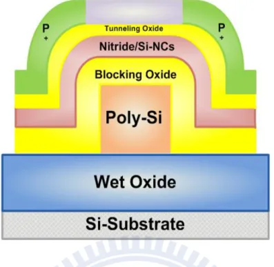
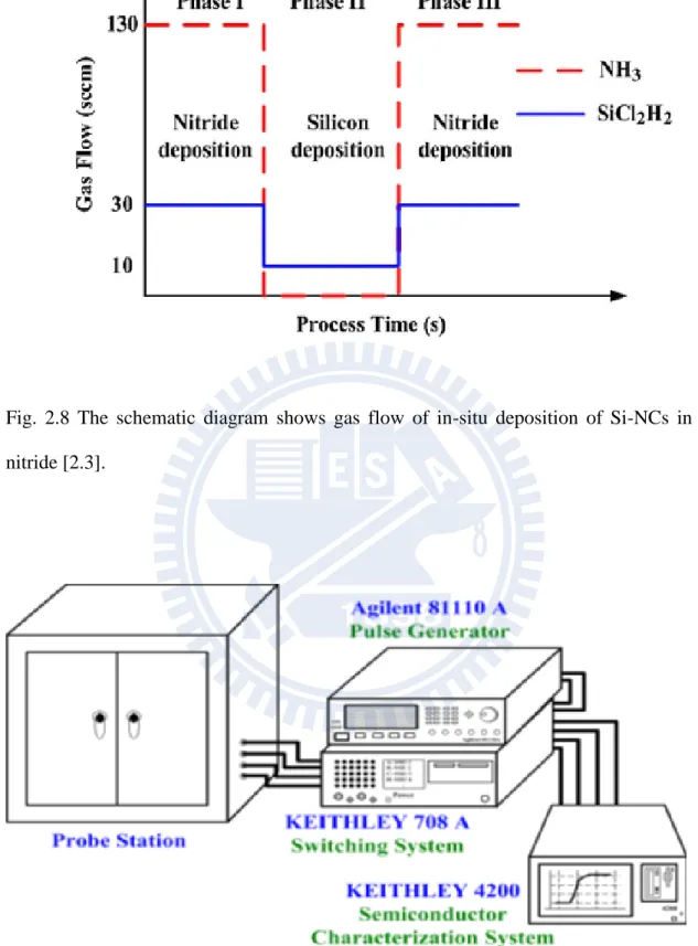
Figure 2.1 to Fig. 2.7 show the schematic of the experimental processes diagrams of the in-situ embedded Si-NCs in silicon-nitride film Si-NCs SONOS memory. Devices were fabricated on n-type (100) 150mm, 8-12 Ω-cm silicon substrates. First, the 500nm thermal oxide was grown on silicon wafer by furnace. Second, 150nm p+-poly-Si was deposited as the gate electrode with boron implantation (70keV, 5 ∗ 1015cm−2). After defining the active regions, the 20nm blocking oxide was thermally grown on p+-poly-Si. Third, in-situ embedded Si-NCs in silicon nitride film
16
formed with three steps, including depositing 3nm nitride film in low pressure chemical vapor deposition (LPCVD) system by using 30sccm NH3 and 130sccm SiCl2H2 at 780℃, forming Si-NCs with 10sccm SiCl2H2, and depositing 4nm nitride film by using 30sccm NH3 and 130sccm SiCl2H2 on Si-NCs as shown in Fig. 2.8. [2.3] Then, 10nm tunneling oxide was thermally grown on nitride film. Next, the 50nm amorphous silicon (α-Si) was deposited by LPCVD with boron doping 5 ∗ 1414cm−2 and 1 ∗ 1515cm−2 respectively. Then, 5nm nickel was deposited by e-beam evaporation and annealed at 520℃. Finally, the contact hole was patterned and 500nm Al was deposited to fabricate the Si-NCs SONOS memories.
2.3 Measurement and Equipment Setup
The measurement setup of this TFT-SONOS device is illustrated in Fig. 2.9, including the electrical characterization system (KEITHLEY 4200), two channel pulse generator (Agilent 8110), low leakage current switch mainframe (KEITHLEY 708A) and the probe station.
KEITHLEY 4200 equipped with programmable source-monitor units (SMU) and provides a high current resolution to pico-ampere range to facilitate the current measurement. Agilent8110A with two pulse channels provides the high timing resolution pulse for the P/E characterization of nonvolatile memory. KEITHLEY 708A configured a 10-input*12-output switching matrix, which can switches the signals from the KEITHLEY 4200 and Agilent 8110A when the device is measured in probe station. Moreover, C++ language is used to achieve the control of the devise measurement instruments.
17
2.4 Operation and Parameter Extraction of TFT-SONOS Memory
2.4.1 Threshold Voltage
The method to determinate the threshold voltage in this thesis is the “constant drain current method” that the voltage at a specific drain current is taken as the threshold voltage (𝑉𝑡ℎ). Typically,
𝐼𝐷𝑁 = 𝐼𝐷/(𝑊𝑒𝑓𝑓 𝐿𝑒𝑓𝑓)
Where 𝐼𝐷𝑁 is the normalize drain current, 𝑊𝑒𝑓𝑓 is effective channel width and 𝐿𝑒𝑓𝑓 is the effective channel length. The threshold voltage is equal to gate voltage when 𝐼𝐷𝑁 = 1𝑛𝐴 in this thesis.
2.4.2 Subthreshold Swing
Subthreshold swing S.S. (V/dec) is defined as: S. S. = 𝑑𝑉𝐺
𝑑(𝑙𝑜𝑔𝐼𝐷) 𝑉𝐺: gate voltage, 𝐼𝐷: drain current
It means the amount of gate voltage required to increase or decrease drain current by one order of magnitude. The subthreshold swing presents devices gate control ability and number of trap states. [2.4-2.5] It might increase with drain voltage (lower gate control) due to short-channel effects such as charge sharing, avalanche multiplication, and punch through-like effect. And it is also relate to trap states due to dangling bonds and oxide defeats such as programming or erasing operation, stress and strain.
18 2.4.3 Source/Drain Resistance
In order to achieve the density and performance specifications of stat-of-the-art VLSI, MOSFEST’s channel length has been scaled down to nanometers range. To control the fabrication of these devices it is necessary to accurately determine channel length. Moreover, this knowledge is required for circuit designs whose performance mainly relies on the use of these scaled devices. In this thesis, La Moneda method [2.6] was used to electrically determine channel length, mobility, and source/drain resistance. The model describes
𝑒𝑓𝑓 =1 + 𝜃(𝑉 𝐺𝑆− 𝑉𝑡ℎ) 𝑅𝑡𝑜𝑡 = 𝐿 − ∆𝐿 𝑊𝑒𝑓𝑓 𝐶𝑜𝑥(𝑉𝐺𝑆 − 𝑉𝑡ℎ)+ 𝜃(𝐿 − ∆𝐿) 𝑊𝑒𝑓𝑓 𝐶𝑜𝑥+ 𝑅𝑆𝐷 = 𝑚 𝑉𝐺𝑆− 𝑉𝑡ℎ+ 𝜃𝑚 + 𝑅𝑆𝐷 The parameters are obtained by curve fitting output resistance measurements over a range of gate biases and channel lengths. Measurements from two gate biases on each of two devices of different channel length are sufficient to obtain a full characterization. Thus, the method is well suited for automated testing because of its simplicity and efficiency.
2.4.4 Fowler-Nordheim (FN) Mechanism
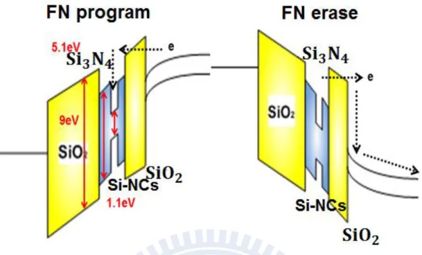
The Fowler-Nordheim (FN) is the flow of electrons through a triangular potential barrier illustrated in Fig. 2.10. FN tunneling mechanism occurs when applying a strong electric field across a thin oxide. In this thesis, the 20V is applied to the gate terminal and the voltage drop across the tunneling oxide make the electrons injecting from channel into trapping layer during programming; the -20V is applied to control gate and electrons detrap from trapping layer during erasing. Using a free-electron gas
19
model for the metal and the WKB approximation for the tunneling probability, one obtains the following expression for current density [2.7-2.8]:
J = 𝑞 3𝐹2 1 𝜋2 2𝜑 𝐵exp [ −4(2𝑚𝑂𝑋)1/2𝜑𝐵3/2 3 𝑞𝐹 ]
Where 𝜑𝐵 is the barrier height, 𝑚𝑂𝑋 is the effective mass of the electron in the forbidden gap of the dielectric, h is the Plank’s constant, q is the electronic charge, and F is the electric field through the oxide.
2.4.5 Pelgrom Plot
Dr. Pelgrom proposed and demonstrated the simple evaluation method of the random variation in 1989 as shown in Fig. 2.11. The method based on simple statistics which described as:
𝜎
𝑡ℎ=
𝐴𝑉𝑇√𝐿𝑊 [2.9]
AVT: the slop beteeen threshold voltage standard devition and device area square root W: channel width, L: channel length.
Since devices scale down, threshold voltage variation is a significant issue. Pelgrom plot can foretell the easy prospect of threshold voltage variation which uses generally.
2.4.6 Arrhenius plot
Arrhenius plot is used to analysis charge loss mechanism. It reported a retention time model with linear variations with temperature. The effective activation energy ( ) to confine the charge loss mechanism were estimated from
20 = 𝜕𝐼𝑛𝑡𝑅
𝜕(𝑘𝑇)1
Where T, 𝑡𝑅 and k are the temperature, the retention time and the Boltzmann constant, respectively. By extracting value, we can determine charge loss reasons from Table 2.1 [2.10].
2.5 Characteristic of Memory
2.5.1 Characteristic of Retention
Retention time describes the ability of devices to store charges after programming at a specific temperature. Generally, the retention time should more than ten years which means the amount of loss charge in storing region must be as minimal as possible. The previous study had reported that retention capability of SONOS memories has to be checked by using accelerated test such that high electric fields or high temperature [2.11-2.13]. In this work, we discuss data retention characteristic after programming with three different temperatures. (25℃, 75℃, 125℃) By measuring the threshold voltage variation, we can find the amount of the excess trapping electrons.
2.5.2 Characteristic of Endurance
Endurance means how many cycles the devices can reversibly and reliably switch. The endurance values reported in the literature range from 10 to 1 ∗ 106 cycles and the endurance record has been 1 ∗ 101 cycles so far [2.14]. The limitation on memories endurance is controlled by two major factors. One is the Time-Dependent-Dielectric-Breakdown (TDDB) characteristics of the charge transfer
21
oxides used for erase and program. The other is threshold voltage level disturbance during program and erase cycles [2.15]. In this thesis, we would find the dominate factor for embedded Si-NCs SONOS memory and solve ways to extend the endurance time.
22
Mechanism Activation Energy (eV)
Tunnel oxide breakdown ≈0.3
ONO ≈0.35
Oxide defects ≈0.6
Cycling induced charge loss ≈1.1 Ionic contamination ≈1.2
Intrinsic charge loss ≈1.4
Table 2.1. JOE E. Brewer reported the value and mechanism relation in 2007 [2.10].
Fig. 2.1. Thermal oxide was grown on silicon wafer, depositing 150nm amorphous silicon and annealed to poly-silicon.
23
Fig. 2.2. Gate was defined and implanted boron with 5 ∗ 1015𝑐𝑚−2 dosage.
Fig. 2.3. Blocking oxide was deposited and used in-situ technique to embed Si-NCs in nitride film, as shown in Fig. 2.2.
24 Fig. 2.4. Tunneling oxide was deposited.
25
Fig. 2.6. Active region was defined and implanted with boron dosage. 1 ∗ 10𝟏𝟓𝑐𝑚−𝟐 and 5 ∗ 10𝟏𝟒𝑐𝑚−𝟐.
Fig. 2.7. Using MILC technique at 520℃, amorphous silicon was recrystallized to poly-silicon.
26
Fig. 2.8 The schematic diagram shows gas flow of in-situ deposition of Si-NCs in nitride [2.3].
Fig. 2.9 The experimental setup for the transfer characteristic and program/erase characteristic of SONOS with Si nanocrystals memory.
27
Fig. 2.10 A schematic of the FN tunneling during programming (left) and erasing (right) in the electric field.
Fig 2.11 Different oxide thickness present in Pelgrom plot. If 𝐴𝑣𝑡= 3.8, then 7nm oxide thickness will have about 400mV variation in threshold voltage. If we want to variation smaller than 100mV, than 𝐴𝑣𝑡value should be choose smaller than one. [2.9]
28
Chapter3
Characteristics of Si-NCs-SONOS Nonvolatile Memory
3.1 Overview
T. Ma et al. reached a conclusion regarding the effect of implantation boron before MILC process which stated the MILC migration rate will double at 550℃ as boron doping concentration 3 ∗ 1015𝑐𝑚−2 in 1000Å non-crystalline silicon film. [3.1]. Lu et al. has reported 𝑁𝑖𝑆𝑖2 formation at a much lower temperature of 250℃ in heavily boron doped Si. This implies that heavy boron doping effectively reduces the formation energy of NiSi2. So any retardation effects induced by implantation damage are somehow compensated due to boron enhancement effect. However, C. Byun et al. found that the MILC migration rate showed a decrease as using boron doping comparing to un-doped α-Si. The decrease in the MILC migration rate results from disturbance of dopant migration through segregation and dopant on NiSi2 layer [3.2-3.3].
We curious about boron would enhance or retardate the nickel diffusion and this
effect would hold in the memory devices. Therefore, we designed two different boron doping concentration (5 ∗ 1014𝑐𝑚−2, 1 ∗ 1015𝑐𝑚−2) devices with MILC process to analyze their physical and electrical properties. In addition, we choose 30s Si-NCs
deposition time in SONOS memory for studying standard. Since T.Y. Chuang has
reported 30s deposition time Si-NCs SONOS memories show excellent electrical
performance, we can decrease other influence factor in memories characteristics
29
3.2 Source/Drain Doping Dependence
3.2.1 X-ray Diffraction (XRD) Analysis
The atomic planes of a crystal cause an incident beam of X-rays to interfere with one another as they leave the crystal. The phenomenon is called X-ray diffraction (XRD). XRD is a nondestructive technique which can identify crystalline phases, crystalline orientation and grain size. As grain size decreases hardness increases and intensity (peaks) become broader [3.8]. Table 3.5 and Fig. 3.3 show the XRD results of poly-silicon channel with different boron doping (5 ∗ 1014𝑐𝑚−2, 1 ∗ 1015𝑐𝑚−2) devices. The average grain size of high to low boron doping device ratio is 2.4. Therefore, poly-silicon grain size can be enhanced by using higher boron doping based on the same thermal budget. The larger grain size in doping boron concentration 1 ∗ 1015𝑐𝑚−2 memory is mostly attributed to boron atoms can reduce the 4% lattice mismatch between c-Si and NiSi2 since they reduce the lattice constant of c-Si. In other words, reduction of lattice mismatch is equal to reduce the strain at the c-Si to NiSi2 interface and inhibit the broken of Ni silicide. As a result, the directional growth behavior of MILC occurs and shows an enhanced growth rate due to the fast migration of 𝑁𝑖𝑆𝑖2 layer without temporary growth halt caused by the breaking NiSi2 [3.1, 3.9-3.10].
3.2.2 Transistor Performance
The current-voltage ( 𝐼𝑑 − 𝑉𝑔 ) characteristics of different boron doping concentration memories were compared in Fig. 3.4(a). The devices with 10μm gate length (L) and 10μm gate width (W) was measured. The red simple represents the drain current versus gate voltage curve with higher boron doping concentration
30
(1 ∗ 1015) and show the lower leakage current, higher on current and better subthreshold slope than the lower doping concentration sample (5 ∗ 1014). Therefore, we think that the high boron doping device can obtain good channel crystalline which is responsible for the improvements of electrical properties of Si-NCs-SONOS memories. The good channel crystalline decrease grain boundaries and trap density at the channel between source and drain regions. Both devices parameters of Si-NCs-SONOS memories are given in Table 3.1.
Transconductance (𝐺𝑚) data was obtained by differentiating 𝐼𝑑− 𝑉𝑔 curve as shown in Fig. 3.4(b). Better 𝐺𝑚 is attained in boron doping concentration 1 ∗ 1015𝑐𝑚−2 memory from gate voltage -4V to -12V. The higher current drive in this Si-NCs SONOS memory is due to large grain size and few grain boundaries.
Pelgrom plot tells the simple prospect of threshold voltage (𝑉𝑡ℎ) variation as shown in Fig. 3.5. For higher boron doping device, the slope is 0.57 V/μm. This means if we want 𝑉𝑡ℎ variation smaller than 200mV, then device width multiple length should larger than 8 𝑚2(L ∗ W ≥ 1
( .2 .57⁄ )2). For lower boron doping, the slope is 1.1 V/μm. This means if we want 𝑉𝑡ℎ variation smaller than 200mV, then device width multiple length should larger than 30 𝑚2(L ∗ W ≥ 1
( .2 1.1⁄ )2). It’s clearly that higher boron doping device shows better uniformity and scaling ability.
Fig. 3.6 shows the subthreshold swing (S.S.) versus channel length. When channel length larger than 6μm, the S.S. are around 400mV/dec , 500mV/dec for high and low doping devices. The lower boron doping device S.S. increases significantly beyond length 6μm. In contrast, higher boron doping device presents better S.S. uniformity which confirms with pelgrom plot result.
31 3.2.3 Program/Erase Characteristics
Fig. 3.7(a) and Fig. 3.7(b) present the FN program window in different voltage bias with width 10μm and length 10μm. Both conditions program window increase with increasing program stress voltage. For 5 ∗ 1014𝑐𝑚−2 doping concentration, memory window are 0.48 V, 1.31V and 1.84V as programming voltage 18V, 20V and 22V, respectively. For 1 ∗ 1015𝑐𝑚−2 doping concentration, memory window are 0.5V, 1.6V and 2V as programming voltage 18V, 20V and 22V, respectively.
Fig. 3.8(a) and Fig. 3.8(b) present the FN program window in different voltage bias with width 10μm and length 10μm. Both conditions erase window increase with increasing erase stress voltage. For 5 ∗ 1014𝑐𝑚−2 doping concentration, memory window are 0.12 V and 1.1V as erasing voltage -18V and -20V. For 1 ∗ 1015𝑐𝑚−2 doping concentration, memory window are 1.1 V and 2V as erasing voltage -18V and -20V.
The higher boron doping device with larger memory window is accordance with the boron enhanced diffusion effect causing longer MILC length, bigger grain size and fewer boundaries. Since we adopted bottom gate SONOS memory, channel inversion is totally dependent on gate to source and gate to drain overlap regions. The higher boron doping device has longer MILC length so channel conduct faster as shown in Fig. 3.10. In addition, larger grain size and fewer boundaries also reduce threshold voltage. So boron doping 1 ∗ 1015𝑐𝑚−2 device gets higher overdrive voltage and presents larger memory windows as adding the same gate bias in boron doping 5 ∗ 1014𝑐𝑚−2 device. Furthermore, both devices subthreshold swing (S.S.) degrade severe as gate voltage increasing. Because higher voltage trapping charges or de-trapping charges damage oxide quality significantly and create more interface traps resulting S.S. degradation.
32
The FN P/E speed characteristics with width 10μm and length 10μm are shown in Fig. 3.9(a) and Fig. 3.9(b). Threshold voltages in the higher doping concentration are given by the curves with open symbols, whereas the curves with filled symbols displayed the lower doping concentration. About 0.1 second we can find both devices totally program, but they don’t totally erase until 1 second. The program speed is faster than erase speed and without saturation effect. The high boron doping device show larger P/E window and faster P/E speed than low boron doping devices. The main reason is larger overlap gate to source and gate to drain regions which directly point out boron enhanced nickel diffusion effect.
3.2.4 The Reverse Read and Forward Read
Fig. 3.11(a) and Fig. 3.11(b) show the feasibility of performing SONOS memory through a forward read and reverse read scheme in a single cell. It is known that the forward read and reverse read can be employed to detect the information stored in programmed bits (drain or source side). However, there almost don’t have threshold voltage difference between forward read and reverse read in two types of doping. This means that the charges are uniformly distribution in Si3𝑁4 storage layer which is the consistent with the FN mechanism prediction.
3.2.5 The Comparison of Source/Drain Resistance and Overlap Length
The source/drain resistance (RSD) and overlap length (∆L) are gate bias dependent as shown in Fig. 3.12. La Moneda et al. purposed a method to extract the above parameters [3.11]. The curve fitting for extracting RSD and ∆L procedures involve three plotting which are discussed on channel length 1μm, 5μm and 10μm devices. The (𝑉𝐺𝑆 − 𝑉𝑡)−1 and mask length (L) are independent variables.
33
The procedure begins by generating first plots of 𝑅𝑚 verse (𝑉𝐺𝑆 − 𝑉𝑡)−1 as shown in Fig. 3.13. The intercept points on y-axis present 𝑅𝑚 = 𝜃 ∗ 𝑚+𝑅𝑆𝐷 values. The second procedure is differential of 𝑅𝑚 and 𝑚, so we can get 𝑅𝑆𝐷 values as shown in Fig. 3.14. Finally, the overlap length can obtain by differential the m (𝑚 =
𝐿−∆𝐿
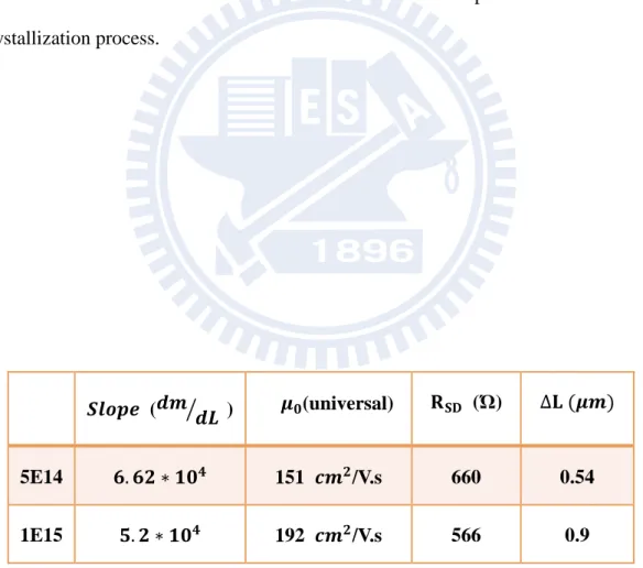
𝑊𝑒𝑓𝑓𝜇𝑜𝐶𝑜𝑥) and L, the intercept point on x-axis is overlap length as shown in Fig. 3.15. Higher doping device has lower source/drain resistance and larger diffusion length as shown in Table 3.2. Doping can decrease resistance between contact material and silicon and longer diffusion length increase the contact area Therefore, higher doping concentration device shows larger on current, better subthreshold swing which confirms the Table 3.1 results.
In order to double check the extraction value of source/drain resistance and overlap length. We calculated the universal mobility ( ) by differential m and L form Fig. 15 as following:
𝑚 = 𝐿 − ∆𝐿
𝑊𝑒𝑓𝑓 𝑜𝐶𝑜𝑥 𝑜 =
1 𝑊𝑒𝑓𝑓𝐶𝑜𝑥𝑑𝑚𝑑𝐿
The Table 3.2 show universal mobility values 192 𝑐𝑚2⁄𝑉 − 𝑠 and 152 𝑐𝑚2⁄𝑉 − 𝑠 for high and low doping devices. Then we obtained field effect mobility ( ) from
𝑑− 𝑉𝑔 graph. By differential 𝐼𝑑− 𝑉𝑔 curve, was calculated by
=
𝑊 𝐿𝐶
𝑜𝑥𝑉
𝐷𝑆=
𝐿 𝑊𝐶𝑜𝑥 .The versus 𝑉𝑔 curves are plotted in Fig. 3.16, the maximum values are 163 𝑐𝑚2⁄𝑉 − 𝑠 and 130 𝑐𝑚2⁄𝑉 − 𝑠 for high and low doping devices. It’s reasonable that smaller than 𝑜 since ignores mobility dependent gate bias factor. The boron doping concentration 1 ∗ 1015𝑐𝑚−2 device has higher mobility over the range of 𝑉𝑔 between -4V to -12V, because boron enhanced nickel directional and faster diffusion leading to large grain size and fewer trap charges scattering. The carrier
34
mobility determines the current drive, the transconductance, and the speed of the transistor. Therefore, many advantages of higher boron doping device are evidenced by the mobility graph in Fig. 3.16.
3.2.6 The Comparison of Off-Leakage
The GIDL current generated when the source/drain of PMOS device is biased at the supply voltage (𝑉𝑆𝑆/𝑉𝐷𝐷) and the gate is biased at zero or positive voltage. Thus, a depletion region is formed in the surface of the overlap region between the gate and source or drain. If the gate biased is positive enough to cause the band bending at the source/drain surface to exceed the silicon bandgap (1.12eV), valence band electrons will start to tunnel to the conduction band, giving rise to a band-to-band tunneling current as shown in Fig. 3.17 [3.12]. The electrons tunneling from the valence band subsequently leave via the substrate and the generated holes enter the drain creating the leakage current, which is the GIDL current as shown in Fig. 3.18.
The tunneling process depends on the electric field and band bending in the gate to source/drain overlap region near the source/drain surface. Since two device under the same gate biased, the overlap region size is the dominate factor. Fig. 3.19 show high and low doping devices GIDL current. The filled samples are current from drain to gate and the open samples are current from source to gate. This means higher doping device with larger overlap region which is the same result as above calculation. The Fig. 3.20 shows average GIDL current for source and drain sides of two different boron doping (5 ∗ 1014𝑐𝑚−2, 1 ∗ 1015𝑐𝑚−2) concentration before MILC process samples and one MILC process before boron doping 5 ∗ 1015𝑐𝑚−2 concentration sample, respectively. We can find three things in Fig. 3.20. First, the MILC process after boron doping devices present larger GIDL current than MILC process before
35
doping device. This is clearly evidence to show boron enhanced diffusion leading large overlap region between source and drain sides. Second, the source side has higher GIDL current than the drain side in three samples. Because the nickel was deposited on the source side, it’s inevitable that small amounts of Ni or NiSi2 precipitates are present and further enhance leakage current. Third, doping 1 ∗ 1015𝑐𝑚−2 concentration device has larger GIDL current difference for source and drain sides than other device. T. Ma and M. Wing have reported MILC rate is found to increase at the highest dose of 3 ∗ 1015𝑐𝑚−2 as shown in Fig. 3.21 [3.1], we think this phenomenon occur at the highest dose of 1 ∗ 1015𝑐𝑚−2 leading to obvious difference between source and drain sides GIDL current.
3.2.7 The Comparison of Retention Characteristics
Fig. 3.22, Fig. 3.22 and Fig. 3.23 show the normalized charge losses as a function of retention time at 25℃, 75℃ and 125℃, respectively. Here, the initial threshold voltage shift (∆𝑉𝑡ℎ ) and the ratio of the normalized charge loss was defined as normalized charge losses (∆𝑉𝑡ℎ(𝑡)/∆𝑉𝑡ℎ ). The charge loss mechanisms of SONOS cells are identified three main discharging paths. One is related to thermal excitation of trapped carriers, the other is due to direct tunneling through the thin tunnel oxide of the ONO stack, and another is trap assisted tunneling. The direct tunneling mechanism is weakly dependent on temperature and will remain negligible also at high temperature. The thermal emission component instead is very sensitive to temperature and to the energy distribution of the trapped charged [3.13].
Constant temperature retention time graph is shown in Fig. 3.22. The thermal emission component only has small influence on devices and both conditions have the same tunneling oxide thickness resulting in similar tunneling probabilities. Therefore,
36
de-trapping process turns out to be mostly dependent on trap assisted tunneling component. High and low doping devices show small charge loss percentages of 3.5% and 3.3% as time of stress increasing to 104 seconds in Fig. 3.22. So they almost have the same number of shallow traps at the interface or electron traps in the tunneling oxide.
After 10k P/E cycles, the charge loss curves of SONOS memories at 75℃ and 125℃ are shown in Fig. 3.23 and Fig. 3.24. For temperature at 75℃, charge loss curves for high and low boron doping devices have similar trends as constant temperature before 102 seconds and the loss percentages increase to 24% and 23.3% as 104 seconds. This is due to thermal emission phenomenon dominate the loss mechanism by changing trap energy after 102 seconds. For temperature at 125℃, the charge loss slightly before 102 seconds for both devices. After 102 seconds, the high and low doping devices charge loss values are 44.3% and 62.6% at 104 seconds. The reason is high temperature causes more deep traps emission resulting in significantly charge loss and dramatically curves dropping. Although higher doping device has the larger overdrive as the same program voltage, it show less charge loss at 125℃. This means higher boron doping device has less deep traps so they present better oxide quality and longer retention time at high temperature than low boron doping device.
The Arrhenius plots of retention time characteristics for window dropping 0.05V and 0.1V appear in the insets of Fig. 3.25. De Salvo et al. [3.14-3.15] reported a retention time model with linear variations as temperature change. Here, the effective activation energy ( ) to confine the charge loss mechanism were estimated from
= ∂ln (𝑡𝑅) ∂(𝑘𝑇)1
![Table 2.2 Summary of Metal Induced Crystallization (MILC) observations. [1.6]](https://thumb-ap.123doks.com/thumbv2/9libinfo/8495726.184924/27.892.136.788.109.320/table-summary-metal-induced-crystallization-milc-observations.webp)
![Table 2.1. JOE E. Brewer reported the value and mechanism relation in 2007 [2.10]](https://thumb-ap.123doks.com/thumbv2/9libinfo/8495726.184924/40.892.137.740.97.969/table-joe-e-brewer-reported-value-mechanism-relation.webp)
![Table 3.4. Both high and low doping devices values approximate 0.6eV which charge loss mechanism are dominated by oxide defects [3.14]](https://thumb-ap.123doks.com/thumbv2/9libinfo/8495726.184924/58.892.219.656.454.990/table-doping-devices-values-approximate-mechanism-dominated-defects.webp)
![Fig. 3.2. The TEM graph of Si-NCs deposited on Si 3 N 4 layer [3.4].](https://thumb-ap.123doks.com/thumbv2/9libinfo/8495726.184924/60.892.142.625.157.980/fig-tem-graph-si-ncs-deposited-si-layer.webp)