應用於助聽器之低電壓低功率三角積分調變器
87
0
0
全文
(2) 應用於助聽器之低電壓低功率三角積分調變器 The Design of Low Voltage, Low Power Sigma-Delta Modulator for Hearing Aids Student : Po-Chen Lin. 研 究 生:林柏成. Advisor : Chau-Chin Su. 指導教授:蘇朝琴 教授. 國 立 交 通 大 學 電 機 與 控 制 工 程 研 究 所 碩 士 論 文. A Thesis Submitted to Department of Computer and Information Science College of Electrical Engineering and Computer Science National Chiao Tung University In partial Fulfillment of the Requirements for the Degree of Master in Electrical and Control Engineering July 2003 Hsinchu, Taiwan, Republic of China. 中 華 民 國 九十四 年 七 月.
(3) 應用於助聽器之低電壓低功率三角積分調變器. 研究生:林柏成. 指導教授:蘇朝琴. 國立交通大學電機與控制工程研究所. 摘要 近年來由於積體電路製程的進步,每個電晶體的尺寸亦隨之降低,使得在晶 片內電路的密度可以愈做愈高。然而,電晶體的臨界電壓並沒有隨著製程的進步 而線性的降低.這將會增加電路設計上的困難,尤其是在深次微米的製程上。因 此,低電壓的電路設計顯得格外重要,亦是未來發展的一大趨勢。 在此論文中,提出一個應用於助聽器之低功率與低電壓的三角積分調變器。 使用反相器(Inverter)做為電容切換式積分器中的運算放大器,用以實現一個三階 的三角積分調變器。為了降低製程偏移的影響,使用一些電路技巧,用以消除運 算放大器的偏移電壓。由於低電壓的系統設計,會使得切換的開關無法正常的導 通或關閉,因此,一般低電壓的電路設計亦會在此介紹。除此之外,因為低電壓 系統對於雜訊的影響較大,所以亦會在所提出的電路架構中做完整的推導。另 外,時脈對開關所造成的雜訊,可以藉由多餘的開關(dummy switches)製造反相 的雜訊以消除單一開關所產生之雜訊。 所提出的電路架構將被實現在 TSMC CMOS 0.18 µ m 的製程,其晶片面積為 0.73µm × 0.74 µm (不包含 PAD),當取樣頻率在 2M Hz、頻寬被設定在 20kHz 及 電壓為 1V 時,可以得到最大之訊號失真雜訊比(SNDR)為 69.01dB,訊號雜訊比 (SNR)為 75.74dB,動態範圍(Dynamic Range)為 76dB。 索引詞彙—三角積分調變器、電容切換式積分器、低電壓、低功率、反相器、偏 移電壓消除。. i.
(4) The Design of Low Voltage, Low Power Sigma-Delta Modulator for Hearing Aids. Student: Po-Chen Lin. Advisor: Chau-Chin Su. Institute of Electrical and Control Engineering Nation Chiao Tung University Abstract In recent years, the dimension scales down with the advance of IC fabrication technology such that the circuit component density is becoming higher and higher. However, the threshold voltage is not scaled down linearly with the dimension. It increases the difficulty of circuit design, especially with the deep sub-micron process. Therefore, the low voltage circuit design is a necessary trend for the future. The design of a low-voltage and low-power sigma-delta modulator is presented for hearing aids application. A third-order single-loop topology is implemented using switched-capacitor circuits with inverter opamp. To decrease process variation in inverter opamp, the technique of offset cancellation is introduced. Due to low voltage system, the switches driving problem and noise issue are also discussed. The clock feed-through noise is reduced using dummy switches. The proposed sigma-delta modulator is implemented using TSMC CMOS 0.18 µ m process with active die area of 0.73µm × 0.74 µm . The peak SNDR is 69.01dB, SNR is 75.74dB, and DR is 76.61dB at a sampling rate of 2M Hz and signal bandwidth of 20k Hz under single 1.0V supply voltage. Index Terms – sigma-delta modulator, switched-capacitor circuits, inverter opamp, low-voltage, low-power, offset cancellation, switches driving.. ii.
(5) 誌謝 在此感謝父母,讓我能無後顧之憂完成碩士兩年的學業。還有要感謝家人在 背後的支持,尤其是我哥不時的告訴我碩士所真正需要學到的是什麼及會與我討 論許多知識,無論是否屬於專業上或是其它領域,這都幫助我拓展更寬的視野。 特別要感謝的是我的指導老師. 蘇朝琴 教授,在老師專業的指導下,讓我. 收益良多,對於所做的專業領域有更深入的了解。除此之外,從老師身上更讓我 學會了對於時間的應用,即使老師的事務繁多,但仍能將事情安排得井然有序, 很值得我佩服及學習。 在此還要感謝一起在實驗室的學長、同學、學弟及助理們。很謝謝仁乾人肯 與我討論我在做專題上所遇到的問題,還有與你討論真善忍的真義。Fuzzy 丸、 ku、鴻文每晚的正義連線,為我沈悶的研究生涯增添了不少樂趣。還有順閔、瑛 佑、懋軒、宗諭、智琦、小 ku、匡良…等,大家一起運動打屁,讓我這兩年學 到不少東西。. 林柏成 20050727. iii.
(6) Table of Contents Abstract ...................................................................................................... ii Table of Contents ...................................................................................... iv Lists of Figures ......................................................................................... vi Lists of Tables ........................................................................................... ix Chapter 1 Introduction .............................................................................1 1.1 Motivation........................................................................................................1 1.2 Basic Concepts of Hearing Aids System .........................................................2 1.3 Thesis Organization .........................................................................................3. Chapter 2 Fundamentals of Sigma-Delta Modulator ...............................5 2.1 Introduction......................................................................................................5 2.2 Overview of Oversampling Converters ...........................................................5 2.3 Noise-Shaped Sigma-Delta Modulators ........................................................ 11 2.4 High-Order Sigma-Delta Modulators ............................................................17 2.5 Performance Metrics......................................................................................21 2.6 Summary ........................................................................................................22. Chapter 3 Design Considerations for Low-Voltage Low-Power Sigma-Delta Modulator.........................................................23 3.1 Introduction....................................................................................................23 3.2 Trends of Low-Voltage Low-Power IC..........................................................23 3.3 Noises in Sigma-Delta Modulator .................................................................24 3.4 Power Dissipation of Integrators ...................................................................27 3.5 Low-Voltage Switch Techniques....................................................................33 3.6 Summary ........................................................................................................39. Chapter 4 A 40- µ W Switched-Capacitor Sigma-Delta Modulator.......40 4.1 Introduction....................................................................................................40 4.2 System Architecture and Specifications.........................................................40 4.3 Implementation of Integrators........................................................................44 4.4 Quantizer........................................................................................................58 iv.
(7) 4.5 Clock Generator .............................................................................................62 4.6 Simulation Results and Layout ......................................................................65 4.7 Test Setup.......................................................................................................67. Chapter 5 Conclusions ...........................................................................71 5.1 The Figure-Of-Merit (FOM)..........................................................................71 5.2 Conclusions....................................................................................................73. Bibliography .............................................................................................74. v.
(8) Lists of Figures Figure 1-1 Signal path block diagram.........................................................................3 Figure 2-1 Two types of quantization (a) midtread and (b) midrise. ..........................6 Figure 2-2 The probability density function for the quantization error. ......................7 Figure 2-3 The power spectral density of quantization noise......................................7 Figure 2-4 Quantizer and its linear model. ..................................................................8 Figure 2-5 Function block of A/D converter................................................................9 Figure 2-6 (a) Conventional Nyquist ADC and (b) Oversampling ADC [5]...............9 Figure 2-7 Quantization noise power spectral density after low-pass filter. .............10 Figure 2-8 The system block diagram of sigma-delta modulator. ............................. 11 Figure 2-9 (a) The architecture and (b) linear model of the sigma-delta modulator. 12 Figure 2-10 The Architecture of first-order sigma-delta modulator. .........................13 Figure 2-11 The Architecture of second-order sigma-delta modulator......................15 Figure 2-12 Noise-shaping transfer function curves. ................................................16 Figure 2-13 General structure of a single quantizer sigma-delta modulator. ............18 Figure 2-14 The high-order interpolative sigma-delta modulator. ............................19 Figure 2-15 A sigma-delta modulator with MASH structure. ...................................20 Figure 2-16 SNDR/SNR versus input signal power. .................................................22 Figure 3-1 Three main noises in a sigma-delta modulator. .......................................24 Figure 3-2 Dangling bonds at the oxide-silicon interface. ........................................25 Figure 3-3 The flicker noise model in a MOSFET. ...................................................25 Figure 3-4 (a) Brown motion and (b) thermal noise at time domain.........................26 Figure 3-5 The thermal noise model in a MOSFET. .................................................26 Figure 3-6 A simplified equivalent model. ................................................................27 Figure 3-7 Switched-capacitor integrator. .................................................................28 Figure 3-8 Continuous-time integrator. .....................................................................31 Figure 3-9 Switched-current integrator......................................................................32 Figure 3-10 Transmission gate conductance at (a) standard and (b) low supply voltage. ......................................................................................................................................34 Figure 3-11 Switch conductance using TSMC CMOS 0.18 µm process.................34 Figure 3-12 A composite switch with low threshold voltage. ...................................35 Figure 3-13 Voltage boosted clock driver. .................................................................36 vi.
(9) Figure 3-14 Voltage doubler. .....................................................................................36 Figure 3-15 The architecture of clock bootstrapped switch. .....................................37 Figure 3-16 Transistor-level implementation of bootstrapped switch.......................37 Figure 3-17. Non-inverting integrator........................................................................38. Figure 3-18 The switched opamp principle. ..............................................................38 Figure 4-1 Single-loop and multiple-feedback topology. ..........................................41 Figure 4-2 System simulation result of the third-order sigma-delta modulator........43 Figure 4-3 Simulation of SNR versus input amplitude.............................................43 Figure 4-4 Pole-zero plot of noise transfer function.................................................44 Figure 4-5 General differential opamp. .....................................................................44 Figure 4-6 (a) CMOS inverter and (b) Cascode inverter. ..........................................45 Figure 4-7 CMOS inverter transfer curve.................................................................45 Figure 4-8 AC response simulation of CMOS inverter. ...........................................47 Figure 4-9 AC response simulation of cascode inverter. ..........................................47 Figure 4-10 Non-inverting integrator with proposed opamp of inverter. ..................48 Figure 4-11 Simulation result of integrator in Figure 4-10 at different corner cases. ......................................................................................................................................48 Figure 4-12 Auto-zeroed integrator using opamp of inverter....................................49 Figure 4-13. Simulation of integrator in Figure 4-12 at different corner cases. ........50. Figure 4-14. Simulation of integrator in Figure 4-12 at different temperatures. .......50. Figure 4-15 Fully differential switched-capacitor integrator.....................................51 Figure 4-16 New integrator with low clock feed-through. ........................................52 Figure 4-17 Switch with dummy transistors..............................................................52 Figure 4-18. Noise model of proposed opamp of inverter. ........................................53. Figure 4-19 Opamp with capacitive feedback and capacitive loading. .....................54 Figure 4-20 Noise model in Figure 4-16 during φ 1 . ................................................55 Figure 4-21 (a) opamp small-signal analysis and (b) noise model during φ 2 ..........56 Figure 4-22. Noise simulation result..........................................................................57. Figure 4-23 The first-order sigma-delta modulator. ..................................................58 Figure 4-24 (a) one-bit quantizer, (b) dynamic compartor , and (c) SR latch. .........59 Figure 4-25. Simulation result of one-bit quantizer. ..................................................59. Figure 4-26 Clock waveform.....................................................................................60 Figure 4-27. Clock feed-through influence................................................................60 vii.
(10) Figure 4-28. Simulation of the first-order sigma-delta modulator for TT case. ........61. Figure 4-29 Simulation results of (a) FF, (b) SS, (c) FS, and (d) SF cases..................62 Figure 4-30 Clock generator circuit...........................................................................63 Figure 4-31. Simulation of Clock generator with voltage boosting...........................63. Figure 4-32. The proposed third-order sigma-delta modulator..................................64. Figure 4-33. Power spectrum of the third-order sigma-delta modulator. ..................65. Figure 4-34 SNDR and SNR versus input amplitude. ..............................................65 Figure 4-35. The layout of third-order sigma-delta modulator. .................................66. Figure 4-36 Experimental test setup. .........................................................................67 Figure 4-37. (a) Precision Audio Analyzer and (b) Logic Analyzer. .........................67. Figure 4-38 AC coupled and input termination circuit..............................................68 Figure 4-39 The application of LM317 regulator. .....................................................68 Figure 4-40 Reference (1.0V) voltage generator. ......................................................69 Figure 4-41 Bypass filter at reference voltage generator...........................................69. viii.
(11) Lists of Tables Table 4-1 Summary of CMOS inverter operation.....................................................46 Table 4-2 The summary of the performance.............................................................66 Table 5-1 The comparison of sigma-delta modulator for the audio application.......72 Table 5-2 The FOM comparison...............................................................................72. ix.
(12) Chapter 1. Introduction. Chapter 1 Introduction. 1.1. Motivation. The recent semiconductor process has a great improvement on the dimension scale down such that the circuit component density is becoming higher and higher. In order to save the chip cost, it trends to integrate all the circuit blocks into a single chip, and becomes a System on Chip (SoC). However, the threshold voltage is not scale down linearly with the dimension. It increases the difficulty of circuit design, especially in the deep sub-micron process. Besides, the power consumption tolerance of each circuit block becomes lower because of the heat dissipation issue. Thus, the power saving is an important issue in order to meet the SoC specification. Also because of portable audio products, low power consumption increases the battery lifetime. According to the power consumption law, the power is in proportion to the square of the supply voltage. Low voltage circuit design is the key to solve the problem of threshold voltage and power saving. Oversampling architecture is a candidate of implementing high resolution A/D converters because it has higher SNR than Nyquist rate A/D converters. Besides, it -1-.
(13) Chapter 1. Introduction. only requires relaxed anti-aliasing filter. Oversampling techniques based on noise shaping are extensively used in implementing the interface between analog and digital signals in VLSI systems, especially in audio applications. The sigma-delta modulator is an attractive approach for the noise shaping because it is insensitive to circuit imperfection and less complicated in analog circuits. Sigma-delta modulator can achieve high resolution because most of the quantization noises can be pushed to out of the signal band. Switched capacitor techniques are used to design a sigma-delta modulator due to their accurate frequency response as well as good linearity and dynamic range. Also, a switched capacitor circuit operates as a discrete-time signal processor. Accurate discrete-time frequency responses are obtained since filter coefficients are determined by capacitance ratios [1]. Besides, the process for capacitors is more accurate than for other device (like resistors). More and more people have hearing loss problem. Hearing loss occurs to may aged people. Hearing loss can be due to aging, exposure to loud noise, diseases and so on. Take USA for example. According to the data of National Center of Health Statistics (NCHS), there are 20 million people with hearing loss in 1991. More recent data compiled by the National Institute on Deafness and Other Communication Disorders, suggest that the number of people with hearing loss is closer 28 million [2]. Thus, developing a low power and low voltage SoC technique is important to increase battery lifetime and convenience for hearing aids. In this thesis, the low voltage, low power sigma-delta modulator is presented. Using of an inverter instead of traditional operation amplifier enables the sigma-delta modulator to achieve tens of micro watts level.. 1.2. Basic Concepts of Hearing Aids System. Currently, hearing aids can be roughly classified as either analog or digital processors [3]. Conventional analog hearing aids are designed with a particular frequency response based on personal audiogram. Analog programmable hearing aids allow user to have settings programmed for different listening environments. Digital programmable hearing aids have the most features of analog programmable aids. It can analyze the environment signals to determine if the sound is noise or speech and then provide a clear signal. In other words, digital programmable hearing aids are self-adjusting. This thesis target at the circuit design of digital programmable hearing -2-.
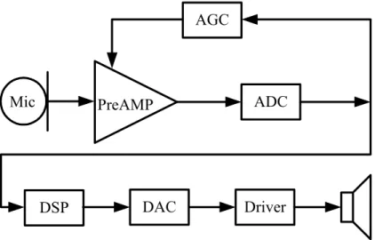
(14) Chapter 1. Introduction. AGC. Mic. ADC. PreAMP. DSP. DAC. Driver. Figure 1-1 Signal path block diagram. aids Figure 1-1 shows the signal path of general digital programmable hearing aids. A preamplifier that includes a gain compression limiting amplifier that amplifies the output of the microphone through auto-gain control (AGC) circuit [4]. The limiter function prevents the large signal from overloading the A/D converter and generating distortion. The digital signal processor (DSP) receives the output of A/D converter and performs the hearing aid signal-processing algorithm. The output of DSP is converted to analog signal by D/A converter. Finally, the analog signal is transferred to earphone by the driver circuit. In order to provide a high resolution signal for DSP, a sigma-delta modulator is used to implement A/D converter in a hearing aid. This thesis presents a low voltage, low power sigma-delta modulator for hearing aids application.. 1.3. Thesis Organization. This thesis is organized into five chapters. In Chapter 1, this thesis and the hearing aids architecture are briefly introduced. In Chapter 2, the basic concepts of quantizer, comparison of oversampling and Nyquist converters, and sigma-delta modulator are introduced. Also, the stability of high-order sigma-delta modulator is considered. Finally, the performance of sigma-delta modulator is presented in detail. In Chapter 3, the noise sources in sigma-delta modulator are introduced and the power efficiency of the integrators is estimated. The solutions for driving the switches are used in low-voltage switched-capacitor circuits are also outlined. -3-.
(15) Chapter 1. Introduction. In Chapter 4, a 40 µ W sigma-delta modulator using inverter opamp is introduced. The inverter opamp can reduce power consumption and chip area. The some techniques are presented to solve the problems using inverter opamp in this chapter. In Chapter 5, the conclusions of this work are summarized. Moreover, the comparisons to the sigma-delta modulators are presented as well.. -4-.
(16) Chapter 2. Fundamentals of Sigma-Delta Modulator. Chapter 2 Fundamentals of Sigma-Delta Modulator. 2.1. Introduction. Some of the fundamental issues in the design of sigma-delta modulators will be reviewed in this chapter. The discussion of oversampling converters is in Section 2.2. It includes the basic concepts of quantization, the comparison of oversampling and Nyquist A/D converters, and oversampling techniques. In Section 2.3 and Section 2.4, noise-shaped sigma-delta modulator and high-order sigma-delta issues are introduced. It discusses how the sigma-delta modulators work. The basic linear models are reviewed. The performance metrics of A/D converter is introduced in Section 2.5.. 2.2. Overview of Oversampling Converters. 2.2.1. Quantization Error. In A/D converters, quantizers are always needed. The analog signal is quantized by quantizer to a of digital code based on different signal levels. The performance of. -5-.
(17) Chapter 2. Fundamentals of Sigma-Delta Modulator. y (digitized). y (digitized). ∆y. ∆y. YFS. YFS. overload. ∆x. XFS T. VQ. + ∆/ 2. overload. x (analog). − ∆/ 2. x (analog) ∆x XFS. +∆/ 2. T. overload. (a). −∆/ 2. VQ. overload. (b). Figure 2-1 Two types of quantization (a) midtread and (b) midrise. the A/D converter depends on the precision of the quantization. According to the quantizer characteristic, it can be classified as either midtread or midrise. Figure 2-1 shows two types of quantizer. The output of midtread is a constant value and that for the midrise is a transition point at the middle of the input range. To understand the characteristics of the quantization error (also called quantization noise), the ramp waveform signal x is given, as the dashed line in Figure 2-1. The corresponding quantization error VQ exhibits sawtooth-like variation and it is depicted at the bottom of Figure 2-1. The quantization error is limited to ± ∆ / 2 where ∆ is the gap between output levels. It is also given by. ∆ = V LSB =. Vref. (2.1). 2N. where Vref is YFS and N is number of bits. The root-mean-square (rms) value of VQ can be derived by. VQ( rms ) =. 2. ∆ 1 T / 2 ⎛−t ⎞ ⎜ ⎟ dt = ∫ T −T / 2 ⎝ T ⎠ 12. (2.2). where T is the period of the sawtooth wave. It is found that the power of the quantization error is in proportion to the square of ∆ . From (2.1) and (2.2), it is obvious that quantization error can be reduced if the number of bits increases. If the. -6-.
(18) Chapter 2. Fundamentals of Sigma-Delta Modulator. fQ ( q ). −∆/ 2. ∆/2. q. Figure 2-2 The probability density function for the quantization error. quantization error VQ is a uniformly distributed random variable, the interfering effect of VQ is similar to thermal noise. The probability density function for such an error signal, f Q (q ) , will be a constant value, as shown in Figure 2-2. The probability density function of the quantization error is given by ∆ ∆ 1 − ≤ q( n ) < 2 2 ∆ f Q (q ) = 0. (2.3). otherwise. However, it must be ensured that the incoming signal does not overload the quantizer. The power spectral density S Q ( f ) of the quantization noise is white and uniformly distributed between ± f S / 2 , as shown in Figure 2-3. From (2.2), the noise power is given by VQ2( rms ) =. ∆2 12. S ( f )df = S Q ( f ) ⋅ f S − fS / 2 Q. =∫. fS / 2. (2.4). Thus, the height of the noise power spectral density equals to ⎛ ∆2 ⎞ 1 ⎟ SQ ( f ) = ⎜ ⎜ 12 ⎟ f S ⎝ ⎠. (2.5). SQ ( f ). − fS / 2. ⎛ ∆2 ⎞ 1 ⎜ ⎟ ⎜ 12 ⎟ f S ⎝ ⎠ fS / 2. f. Figure 2-3 The power spectral density of quantization noise.. -7-.
(19) Chapter 2. Fundamentals of Sigma-Delta Modulator. e(n) x(n). y(n) x(n). y(n). Quantizer. Figure 2-4 Quantizer and its linear model. From (2.5), the power spectral density is inversely proportional to the sampling frequency. If the input signal is a sinusoidal waveform between zero and maximum. (. ). full-scale, which equals to 2 N (∆ / 2 ) , and the rms value is 2 N ∆ / 2 2 . Thus, the SNR is given by ⎛P SNR = 10 log ⎜ in ⎜ PQ ⎝. ⎞ ⎛V ⎞ ⎟ = 20 log ⎜ in( rms ) ⎟ ⎟ ⎜ VQ( rms ) ⎟ ⎠ ⎝ ⎠. ( ). ⎛3⎞ = 10log 2 2N + 10 log ⎜ ⎟ ⎝2⎠ = 6.02N + 1.76. (2.6). The above equation gives the best possible SNR for an N-bit A/D converter. However, the idealized SNR decrease from this best possible value for reduced input signal levels. The SNR values could be improved through the use of oversampling techniques which also means higher sampling frequency. In other words, the input signal’s bandwidth is much lower than the Nyquist rate. The quantization noise can be regarded as an independent additive white-noise signal. Thus, a linear model is made about the statistical property of quantization error, e(n ) , as shown in Figure 2-4. This model is helpful to analysis of sigma-delta. modulators.. 2.2.2. Comparison of Oversampling and Nyquist Converters. The function block of the A/D converter is shown in Figure 2-5. The anti-aliasing filter limits the bandwidth of the input signal and keeps the out of band noise from entering the signal baseband in the sampling process. The analog signal is then sampled in discrete time by a sample-and-hold. Each sampled data is converted to the corresponding digital code by the amplitude quantizer. The design of the digital signal processor depends on the type of the converter. Figure 2-6 shows the comparison of frequency spectrum between a conventional -8-.
(20) Chapter 2. Fundamentals of Sigma-Delta Modulator. Analog Analog Input. Antialiasing Filter. Digital. Sample & Hold. Digital Signal Processor. Amplitude Quantizer. Digital Output. Figure 2-5 Function block of A/D converter.. Transition band Anti-aliasing filter fS = f N. f B 0. 5 f S. Signal Bandwidth Transition band Anti-aliasing filter. Amplitude. Amplitude. Signal Bandwidth. f. fB. (a). fN. 0 .5 f S. f S = Mf N. f. (b). Figure 2-6 (a) Conventional Nyquist ADC and (b) Oversampling ADC [5]. Nyquist A/D converter and an oversampling A/D converter. The bandwidth of the input signal is shown by the rectangle with diagonal lines. The upper limit of the frequency is indicated by f B . In Figure 2-6 (a), the sampling rate is equal to the Nyquist rate ( f N ). It is made as close to 0.5 f N as possible to achieve maximum signal bandwidth ( f B ). In Figure 2-6 (b), the Nyquist rate is much less than the sampling rate. Anti-aliasing filter requirements of the oversampling A/D converters are much more relaxed than those of Nyquist rate converters. The reason for this is that the sampling frequency is much higher than the Nyquist rate in oversampling converters. Also, the transition band is quite wide and the transition is smooth so a simple first-order or second-order analog filters are usually sufficient to meet the relaxed anti-aliasing requirements [5]. Therefore, the less complex filter is adapted into the design of the anti-aliasing filter using an oversampling A/D converter.. 2.2.3. Oversampling Technique. Oversampling means that the sampling frequency exceeds Nyquist frequency. In other words, the sampling frequency is greater than twice the signal bandwidth. And the oversampling ratio (OSR) is defined as. -9-.
(21) Chapter 2. OSR ≡. Fundamentals of Sigma-Delta Modulator. fS 2 fB. (2.7). For a sinusoidal input signal, the maximum signal power is square of rms value. (. ). ( 2 N ∆ / 2 2 ) and is rewritten as 2 2 2N ⎞ ⎟ =∆ 2 ⎟ 8 ⎠. ⎛ ∆2 N PS = ⎜ ⎜2 2 ⎝. (2.8). For an oversampling system, the input signal with frequency below the bandwidth ( f B ) can pass through the lowpass filter without any decay. But, the out-of-band quantization noise is filtered out, as shown in Figure 2-7. Thus, the quantization noise power is given by. PQ = ∫. fS / 2. 2. − fS / 2. = 2 fB ⋅. S Q ( f ) ⋅ H ( f ) df = ∫. fB. − fB. ∆2 1. =. 12 f S. S Q ( f )df. ∆2 ⎛ 1 ⎞ ⋅⎜ ⎟ 12 ⎝ OSR ⎠. (2.9). It can be found that the quantization noise power is reduced half or equivalently 3dB as OSR is doubled. The maximum SNR value can be calculated by 2.8) and (2.9) as. ⎛P SNR = 10 log ⎜ S ⎜ PQ ⎝. ⎛ ∆2 2 2 N ⎞ ⎜ ⎟ ⎞ ⎛ 3 ⋅ 2 2 N ⋅ OSR ⎞ ⎜ ⎟ 8 ⎜ ⎟ ⎟ = 10 log 10 log = ⎜ 2 ⎟ ⎟ ⎜ ⎟ 2 ⎠ ⎝ ⎠ ⎜ ∆ ⋅ ⎛⎜ 1 ⎞⎟ ⎟ ⎜ 12 OSR ⎟ ⎝ ⎠ ⎝ ⎠. ( ). ⎛3⎞ = 10log 2 2 N + 10 log ⎜ ⎟ + 10 log (OSR ) ⎝2⎠ = 6.02 N + 1.76 + 10 log (OSR ). (2.10). The first two terms are the same as (2.6) from an N-bit quantization without oversampling and the final term is due to the use of oversampling techniques. The. SQ ( f ) ⎛ ∆2 ⎞ 1 ⎜ ⎟ ⎜ 12 ⎟ f S ⎝ ⎠ − fS / 2. − fB. fB. fS / 2. f. Figure 2-7 Quantization noise power spectral density after low-pass filter. - 10 -.
(22) Chapter 2. Fundamentals of Sigma-Delta Modulator. oversampling techniques have an improvement of 3dB/octave or 0.5-bit/octave. In other words, if the oversampling ratio is increased by a factor of 4, the resolution can be improved by one bit. Thus, increasing OSR can improve SNR. However, oversampling is not an attractive way because higher sampling frequency and severe linearity are required for high resolution. Hence, the noise-shaped method will be introduced in the next section. It provides a reasonable oversampling frequency to achieve much higher dynamic range.. 2.3. Noise-Shaped Sigma-Delta Modulators. 2.3.1. Introduction to Noise-Shaped Sigma-Delta Modulators. Although oversampling technique can improve SNR value to achieve high resolution A/D converters, the extremely high sampling frequency is needed. To achieve reasonable sampling frequency and higher dynamic range, the feedback architecture is used to obtain the noise-shaping function. The oversampling converters with noise-shaping technique remove much noise away from the signal band. The oversampling converters with noise-shaping technique are implemented as sigma-delta modulator. Figure 2-8 shows the system block diagram of sigma-delta modulator. The analog signal, xin (t ) , is limited in the signal band by anti-aliasing filter to prevent the aliasing of high frequency noise into the signal band. After the anti-aliasing filter, the band limited signal, x(t ) , is oversampled and processed by the sigma-delta modulator. The sigma-delta modulators are usually implemented by a switched-capacitor circuits and then the analog signal is transformed into digital signal, x(n ) . Finally, the digital signal is converted into digital code by decimation filter. A general architecture of sigma-delta modulator with noise-shaping and its linear. Analog Analog Input. x in (t ). Digital. Anti-aliasing Sigma-Delta Filter Modulator x (n ) x (t ). Low-Pass Filter. Down Sampling. xn (t ). Decimation Filter. Figure 2-8 The system block diagram of sigma-delta modulator.. - 11 -. Digital Output.
(23) Chapter 2. + -. u(n). Fundamentals of Sigma-Delta Modulator. X(n). H(Z). Quantizr. Y(n). D/A Converter. (a) e(n) u(n). +. H(Z). X(n). +. Y(n). (b) Figure 2-9 (a) The architecture and (b) linear model of the sigma-delta modulator. model are shown in Figure 2-9. This feedback topology is analogous to the amplifier constructed by the feedback of the opamp. The feedback reduces the low frequency noise when the opamp gain is high enough. At high frequency, the noise is not reduced due to low opamp gain. In other word, a large gain in forward path can lessen the quantization error [6]. The feedback gain equal to unit is utilized to prevent the DAC errors from influencing the performance of sigma-delta modulator. Hence, a great effort should be devoted to the linearity of the DAC for high resolution converters, especially in multi-bit sigma-delta modulator. Single-bit sigma-delta modulator is a good method to solve the linearity requirement of DAC due to only two output levels. Considering the linear model in Figure 2-9 (b), there are two independent inputs. The signal transfer function S TF and noise transfer function N TF can be calculated as. STF ( z ) ≡. Y (z ) H (z ) = U (z ) 1 + H (z ). (2.11). N TF ( z ) ≡. Y (z ) 1 = E (z ) 1 + H (z ). (2.12). From (2.12), the zeros of the noise transfer function, N TF ( z ) , is equal to the poles of H ( z ) . Since the signal transfer function, S TF ( z ) , approaches unity and the noise. - 12 -.
(24) Chapter 2. Fundamentals of Sigma-Delta Modulator. transfer function, N TF ( z ) , approximates zero when H ( z ) goes to infinite. Depending on S TF (z ) and N TF ( z ) , the output signal can be derived as Y ( z ) = STF ( z ) ⋅ U ( z ) + N TF ( z ) ⋅ E ( z ). =. (2.13). H (z ) 1 U (z ) + E (z ) 1 + H (z ) 1 + H (z ). It is desired to choose an adapted H ( z ) with large gain from 0 to signal frequency band. With such a choice, the signal transfer function, S TF (z ) , will approximate unity over the signal frequency band and the noise transfer function, N TF ( z ) , will approximate zero over the same band. Hence, the quantization noise is reduced over the signal frequency band.. 2.3.2. First-Order Sigma-Delta Modulator. Figure 2-10 shows the architecture of a first-order sigma-delta modulator. To realize first-order noise-shaping, the noise transfer function, N TF ( z ) , should have a zero at dc (i.e., z=1) so it is high pass for the quantization noise [1]. Because the zeros of N TF ( z ) are equal to the poles of H ( z ) , H ( z ) with noise-shaped function is given by. H (z ) =. 1 z −1 = z − 1 1 − z −1. (2.14). Then, the signal transfer function, S TF ( z ) , can be derived as. STF =. H (z ) = z −1 1 + H (z ). (2.15). And the noise transfer function, N TF ( z ) , is. N TF =. u(n). + -. 1 = 1 − z −1 1 + H (z ). (2.16). x(n ). z −1 1− z −1. Quantizr. Y(n). Figure 2-10 The Architecture of first-order sigma-delta modulator.. - 13 -.
(25) Chapter 2. Fundamentals of Sigma-Delta Modulator. Thus, the output of sigma-delta modulator is. (. ). Y (z ) = z − 1 ⋅ U (z ) + 1 − z − 1 ⋅ E (z ) To. find. the. magnitude. of. the. noise. (2.17). transfer. function,. N TF ( z ) ,. let. z = e jωT = e j 2πf / f S . Thus, N TF (ω ) = 1 − e jωT =. e jωT / 2 − e − jωT / 2 ⋅ 2 j ⋅ e − jωT / 2 2j. ⎛ω ⎞ = sin⎜ ⎟ ⋅ 2 j ⋅ e − jωT / 2 ⎝2⎠ ⎛ ⎛ω ⎞ ⎛ω ⎞ ⎛ ω ⎞⎞ = sin⎜ ⎟ ⋅ 2 j ⋅ ⎜⎜ cos⎜ ⎟ − j sin⎜ ⎟ ⎟⎟ ⎝2⎠ ⎝ 2 ⎠⎠ ⎝ ⎝2⎠ ⎛ ⎛ω ⎞ ⎛ ω ⎞ ⎛ ω ⎞⎞ = ⎜⎜ 2 sin 2 ⎜ ⎟ + j 2 sin⎜ ⎟ cos⎜ ⎟ ⎟⎟ ⎝2⎠ ⎝ 2 ⎠ ⎝ 2 ⎠⎠ ⎝. (2.18). The magnitude of noise transfer function is ⎛ω ⎞ ⎛ω ⎞ ⎛ω ⎞ N TF (ω ) = 4 sin 4 ⎜ ⎟ + 4 sin 2 ⎜ ⎟ cos 2 ⎜ ⎟ ⎝2⎠ ⎝2⎠ ⎝2⎠. ⎛ω ⎞ = 2 sin⎜ ⎟ ⎝2⎠. (2.19). From (2.5) and (2.19), the noise power is derived as. S (f − fB / 2 Q fB / 2. PQ = ∫. ) ⋅ H ( f ) 2 df. ⎛ ∆2 1 ⎞ ⎛ ⎜ ⎟ ⋅ ⎜ 2 sin⎛⎜ πf ⋅ ⎜f − f B ⎜ 12 f ⎟ ⎜ S ⎠ ⎝ ⎝ S ⎝. =∫. fB. ⎞⎞ ⎟⎟ ⎟df ⎟ ⎠⎠. ⎛ πf If the approximation that f B << f S (i.e. OSR>>1), so that sin⎜⎜ ⎝ fS. (2.20) ⎞ ⎛ πf ⎟⎟ ≈ ⎜⎜ ⎠ ⎝ fS. ⎞ ⎟⎟ . Also ⎠. (2.20) can be derived as ⎛ ∆2 ⎞⎛ π 2 ⎟⎜ PQ ≅ ⎜ ⎜ 12 ⎟⎜ 3 ⎝ ⎠⎝. ⎞⎛ 2 f B ⎟⎜ ⎟⎜⎝ f S ⎠. 3 ⎛ ∆2π 2 ⎞ ⎟⎟ = ⎜ ⎜ 36 ⎠ ⎝. Hence, the maximum SNR is derived as. - 14 -. ⎞⎛ 1 ⎞ 3 ⎟⎜ ⎟ ⎟⎝ OSR ⎠ ⎠. (2.21).
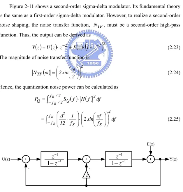
(26) Chapter 2. ⎛P SNR = 10 log ⎜ S ⎜ PQ ⎝. Fundamentals of Sigma-Delta Modulator. ⎞ ⎛ ⎟ ⎜ ∆2 2 2 N ⎟ ⎜ ⎞ 8 ⎟ = 10 log ⎜ ⎟ 3⎟ ⎟ 2 2⎞ ⎛ ⎜ ∆ π 1 ⎛ ⎞ ⎠ ⎟⋅⎜ ⎜⎜ ⎟ ⎟ ⎜ ⎜ 36 ⎟ ⎝ OSR ⎠ ⎟ ⎠ ⎠ ⎝⎝. ( ). ⎛ 3 ⎞ ⎛3⎞ ( = 10log 2 2 N + 10 log ⎜ ⎟ + 10 log ⎜⎜ OSR )3 ⎟⎟ ⎝2⎠ ⎝π 2 ⎠ = 6.02 N + 1.76 − 5.17 + 30 log (OSR ). (2.22). From (2.22), a first-order sigma-delta modulator has an improvement of 9dB, or equivalently, 1.5 bits in SNR while OSR is doubled.. 2.3.3. Second-Order Sigma-Delta Modulator. Figure 2-11 shows a second-order sigma-delta modulator. Its fundamental theory is the same as a first-order sigma-delta modulator. However, to realize a second-order noise shaping, the noise transfer function, N TF , must be a second-order high-pass function. Thus, the output can be derived as. (. Y ( z ) = U ( z ) ⋅ z −2 + E ( z ) ⋅ 1 − z −1. )2. (2.23). The magnitude of noise transfer function is. ⎛ ⎛ ω ⎞⎞ N TF (ω ) = ⎜⎜ 2 sin⎜ ⎟ ⎟⎟ ⎝ 2 ⎠⎠ ⎝. 2. (2.24). Hence, the quantization noise power can be calculated as. S (f − fB / 2 Q. PQ = ∫. fB / 2. ) ⋅ H ( f ) 2 df. f B ⎛ ∆2. ⎛ πf 1 ⎞⎟ ⎛⎜ ⎜ =∫ ⋅ ⋅ ⎜ 2 sin⎜⎜ − f B ⎜ 12 f ⎟ S ⎠ ⎝ ⎝ fS ⎝. 4. ⎞⎞ ⎟⎟ ⎟ df ⎟ ⎠⎠. (2.25). E(z) U(z). + -. z −1 1− z −1. + -. z −1 1 − z −1. +. 2. Figure 2-11 The Architecture of second-order sigma-delta modulator.. - 15 -. Y(z).
(27) Chapter 2. NTF ( f ). Fundamentals of Sigma-Delta Modulator. Second-order First-order No noise shaping. f. fS 2. fB. fS. Figure 2-12 Noise-shaping transfer function curves. ⎛ πf As the approximation in previous section, due to sin⎜⎜ ⎝ fS. ⎞ ⎛ πf ⎟⎟ ≈ ⎜⎜ ⎠ ⎝ fS. ⎞ ⎟⎟ , the quantization ⎠. noise power in the signal band can be derived as. ⎛ ∆2π 4 PQ ≅ ⎜ ⎜ 60 ⎝. ⎞⎛ 1 ⎞ 5 ⎟⎜ ⎟⎝ OSR ⎟⎠ ⎠. (2.26). Hence, the maximum SNR is derived as ⎛ ⎜ ∆2 2 2 N ⎜ ⎛P ⎞ 8 SNR = 10 log ⎜ S ⎟ = 10 log ⎜ ⎜ PQ ⎟ 2 4 ⎜ ⎛ ∆ π ⎞ ⎛ 1 ⎞5 ⎝ ⎠ ⎟⋅⎜ ⎜⎜ ⎟ ⎜ ⎜ 60 ⎟ ⎝ OSR ⎠ ⎠ ⎝⎝. ⎞ ⎟ ⎟ ⎟ ⎟ ⎟ ⎟ ⎠. ( ). ⎛ 5 ⎞ ⎛3⎞ ( OSR )3 ⎟⎟ = 10log 2 2 N + 10 log ⎜ ⎟ + 10 log ⎜⎜ ⎝2⎠ ⎝π 4 ⎠ = 6.02 N + 1.76 − 12.9 + 50 log (OSR ). (2.27). The above equation shows that an improvement of 15dB, or equivalently, 2.5 bits is achieved for the second-order noise-shaping while the OSR is doubled. Figure 2-12 shows that the second-order modulator has steeper shaping slope for the noise in the signal band than the first-order modulator. In other words, the noise power decreases as the noise-shaping order increase. However, the out-of-band noise increases for the higher-order modulators.. - 16 -.
(28) Chapter 2. Fundamentals of Sigma-Delta Modulator. 2.4. High-Order Sigma-Delta Modulators. 2.4.1. Introduction to High-Order Sigma-Delta Modulators. In a sigma-delta modulator, the order of noise transfer function determines how much noise is placed outside the signal frequency band. The high-order signal and noise transfer function can be derived by the similar method as the former modulators. Thus, the general form for the output of the Lth-order noise-shaping modulator can be given by. (. Y ( z ) = U ( z ) ⋅ z − L + E ( z ) ⋅ 1 − z −1. )L. (2.28). The quantization noise power in the signal frequency band can be derived as. S (f − fB / 2 Q. PQ = ∫. fB / 2. )⋅ H ( f ). 2. 2 2 L ⋅ ∆2 1 f B ⎛ πf ⎜ ≅ ⋅ 12 f S ∫− f B ⎜⎝ f S =. ∆2 π 2 L ⎛ 1 ⎞. ⎛ ∆2 1 ⎞ ⎛ ⎟ ⋅ ⎜ 2 sin⎛⎜ πf df = ∫ ⎜ ⋅ ⎜f − f B ⎜ 12 f ⎟ ⎜ S ⎠ ⎝ ⎝ S ⎝ fB. ⎛ ∆2 ⎞⎛ π 2 L ⎞⎛ 2 f B ⎞ ⎟⎜ ⎟⎜ ⎟⎟df = ⎜ ⎟⎜⎝ f S ⎜ ⎟ ⎜ 12 2 L 1 + ⎠ ⎠ ⎠⎝ ⎝. ⎞ ⎟⎟ ⎠. ⎞⎞ ⎟⎟ ⎟ ⎟ ⎠⎠. 2L. df. 2L +1. 2 L +1. ⎟ ⎜ 12 2 n + 1 ⎝ OSR ⎠. (2.29). Thus, the maximum SNR for the Lth-order modulator is. ⎞ ⎛ ∆2 2 2 N ⎟ ⎜ ⎛ PS ⎞ ⎟ ⎜ 8 ⎟ = 10 log ⎜ SNR = 10 log ⎜ 2 L +1 ⎟ ⎜ PQ ⎟ ⎟ ⎜ ∆2 π 2 L ⎛ 1 ⎞ ⎝ ⎠ ⎟ ⎜ 12 2n + 1 ⎜ OSR ⎟ ⎠ ⎝ ⎠ ⎝. ( ). (. ⎛ 2L + 1 ⎞ ⎛3⎞ ⎟⎟ + 10 log OSR 2 L +1 = 10log 2 2 N + 10 log ⎜ ⎟ + 10 log ⎜⎜ 2 L ⎝2⎠ ⎠ ⎝ π ⎛ 2L + 1 ⎞ ⎟⎟ + (20 L + 10 ) log (OSR ) = 6.02 N + 1.76 + 10 log ⎜⎜ ⎝ π 2L ⎠. ). (2.30). The above equation shows that an Lth-order noise-shaping modulator improves the SNR by 6L+3 dB as doubling the OSR, or equivalently L+0.5 bits/octave. However, the high-order sigma-delta modulator has a system stability issue. The following sections will describe stability considerations and two approaches (single-loop and multi-stage noise noise-shaping) for high-order sigma-delta modulator.. - 17 -.
(29) Chapter 2. 2.4.2. Fundamentals of Sigma-Delta Modulator. Stability Considerations in High-Order Modulator. Figure 2-13 shows a general structure of the single quantizer sigma-delta modulator. The linear model of the single quantizer modulator predicts that the stability of the modulator is determined by the loop gain, which is determined by the noise transfer function, N TF ( z ) . However, this argument ignores the effect of nonlinear quantizers. For example, if the input signal is so large such that the input to the first integrator is positive at every time step. Finally, the output of the integrator will monotonically increase without bound and the loop filter will be unstable [7]. Thus, the range of input magnitude is also an important factor in system stability for a high-order sigma-delta modulator. The proper and stable modulator operation is assured if the loop filter remains linear and the internal quantizer is not severely overloaded. Since the stable input range of a sigma-delta modulator is primarily determined by the N TF ( z ) and the number of bits in single quantizer, the stability of single-bit and multi-bit quantizers will be discussed. According to the above argument, the N TF ( z ) is all one needs to know to describe the stability properties of a single-bit modulator. However, the properties of N TF ( z ) are not necessary and sufficient requirements for the stable operation. Thus,. the most widely-used approximate criterion is the Lee criterion [8] [9]: A single-bit sigma-delta modulator with a noise transfer function, N TF (z ) , is likely to be stable if max N TF ( e jω ) < 1.5 . ω. Note that this single-bit criterion is neither necessary, nor sufficient. Nevertheless, due to its simplicity, it is of some use [7].. U. Loop Filter. X. Quantizer. Y. Figure 2-13 General structure of a single quantizer sigma-delta modulator.. - 18 -.
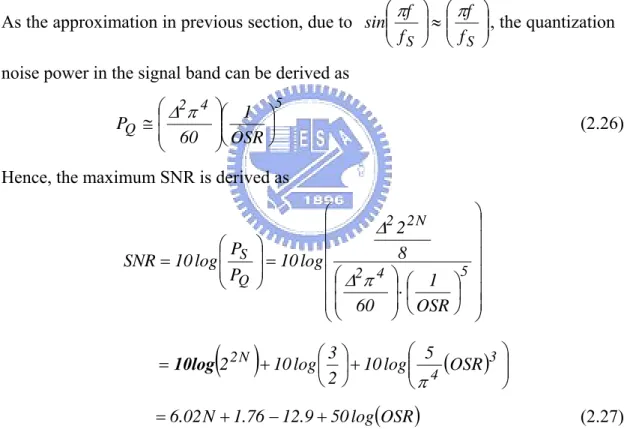
(30) Chapter 2. Fundamentals of Sigma-Delta Modulator. For the multi-bit sigma-delta modulators, the following theoretical result can be useful: Considering a modulator with an M-step (i.e. (M+1)-level) quantizer. Let the initial input y(0) to the quantizer be within its linear (no-overload) range. Then, the modulator is guaranteed not to experience overload for any input u(n) such ∞. that max u(n ) ≤ M + 2 − n 1 , where n 1 = ∑n=0 n(n ) . Here, n(n) is the n inverse z-transform of the noise transfer function N TF (z ) . It is easy to use the above rule to establish a modulator which is implemented with stable noise transfer function.. 2.4.3. Single-Loop High-Order Sigma-Delta Modulator. A high-order sigma-delta modulator can be constructed by connecting a series of the integrators in a single-loop. There are many different single-loop topologies to overcome the stability problem of the modulators. Figure 2-14 shows a high-order interpolative sigma-delta modulator. This architecture reduces the component sensitivity depending on inserting resonators to adjust the zeros of the noise transfer function in the signal band. However, the unavoidable spurious tones appear in the signal band and the dynamic range is decreased due to multi-path of feedback and feedforward. Hence, to increase dynamic range, the architecture is modified with. bi = 0 for i > 1 and g i = 0 [10]. Of course, the integrators are modified as well. u(n). b1. b2. b3. b4. b5. g1 +. a1. -. z −1 1− z −1. +. a2. -. 1 1− z −1. g2 +. -. z −1 1− z −1. a3. +. a4. -. 1 1− z −1. +. -. z −1 1− z −1. a5. Y(n). Figure 2-14 The high-order interpolative sigma-delta modulator.. - 19 -.
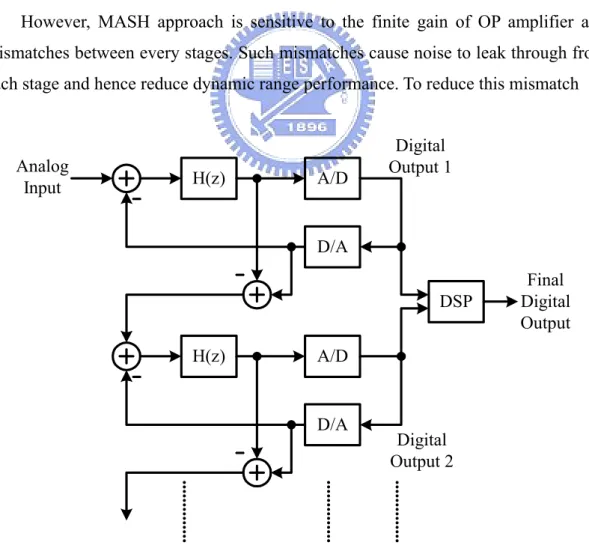
(31) Chapter 2. 2.4.4. Fundamentals of Sigma-Delta Modulator. Multi-Stage Noise-Shaping Sigma-Delta Modulator. Another approach for realizing high-order modulators is to use a cascade-type structure where overall high-order modulator is constructed using first-order or second-order modulator [1]. Since the lower-order modulators are more stable, the overall system should remain stable. This architecture has been called MASH (i.e.. Multi-stAge noise SHaping). Figure 2-15 shows a sigma-delta modulator with MASH structure. The quantization noise of the first stage can be processed by the following stage. The output of the second modulator is combined with the first modulator output to cancel the first modulator error. Hence, the only quantization noise appears in the output of the last stage in an ideal modulator with MASH structure. The advantage of a MASH approach is that high-order noise-shaping can be achieved using low-order modulators. The low-order modulators are more stable as compared to a high-order single-loop structure. However, MASH approach is sensitive to the finite gain of OP amplifier and mismatches between every stages. Such mismatches cause noise to leak through from each stage and hence reduce dynamic range performance. To reduce this mismatch. Analog Input. H(z). A/D. Digital Output 1. D/A DSP H(z). A/D. D/A. Digital Output 2 ............... ............... ............... Figure 2-15 A sigma-delta modulator with MASH structure.. - 20 -. Final Digital Output.
(32) Chapter 2. Fundamentals of Sigma-Delta Modulator. problem, the first stage is often chosen to be a higher-order modulator such that any noise leak-through does not have a serious effect[1].. 2.5. Performance Metrics. 2.5.1. Resolution. The resolution of a converter is defined to be the number of distinct analog levels corresponding to the different digital expression. Resolution is usually expressed by the base 2 logarithm. That is, there are 2 N distinct analog levels it can resolve for a resolution of N-bit. Resolution is usually affected by the noise and the nonlinearity of the quantization or analog circuits. Hence, the real resolution of a converter will be a little degradation. Sometimes it is also called effective number of bits (ENOB).. 2.5.2. Signal-to-Noise Ratio. The signal-to-noise ratio (SNR) is the ratio of signal power to noise power in the system. In a sigma-delta modulator, the SNR value is measured at the output of modulator. The noise sources include all noise in a converter except the noise of harmonic distortion. The peak value of the SNR is also the performance of the system.. 2.5.3. Signal-to-Noise plus Distortion Ratio. The signal-to-noise plus distortion ratio (SNDR) is the ratio of the signal power to the sum of all noise power and the harmonic distortion. The peak SNDR is an important criterion to evaluate the capability and the acceptable linearity of a sigma-delta modulator in the signal band. Note that the peak SNDR is frequency dependent and can be used to measure the degradation of the modulator performance as the input signal increases in frequency.. 2.5.4. Dynamic Range. Figure 2-16 shows that SNDR/SNDR versus the input signal power. Dynamic. range (DR) denotes the range of the input signal amplitude from which useful output can be obtained from a sigma-delta modulator system. The definition of DR is the difference between the input signal level of peak SNR and the input level where x-axis intercepts to the SNDR curve. The minimum detectable input signal power is at SNDR = 0 dB . If the noise power is independent of the signal amplitude, the dynamic. range would be equal to the SNR in the full range. - 21 -.
(33) Chapter 2. Fundamentals of Sigma-Delta Modulator. Peak SNR. 100. SNDR/SNR (dB). 90 80 Overload. 70 60. Dynamic Range. 50 40 30 20. SNR SNDR. 10. -100 -90 -80 -70 -60 -50 -40 -30 -20 -10 0 Normalized Input Power (dB). Figure 2-16 SNDR/SNR versus input signal power.. 2.6. Summary. The sampling rate of Nyquist A/D converters is only twice of the signal band. However, it is difficult to achieve high resolution A/D conversion due to requirements of accurate anti-aliasing filters. The oversampling technique is a good approach to achieve high resolution A/D converters. The sigma-delta modulator is the most used architecture in the oversampling A/D converters. There are two types of quantizers in the sigma-delta modulator. One is a single-bit quantizer and another is a multi-bit quantizer. The quantization noise power of single-bit quantizer is higher than the multi-bit quantizer. However, multi-bit quantizers have much more issues than single-bit quantizers such as linearity, offset, and gain error. In order to achieve high resolution A/D conversion, high OSRs or high-order sigma-delta modulators are required. High OSR sigma-delta modulators need to have better component matching rate. High-order sigma-delta modulators have the stability problems.. - 22 -.
(34) Chapter 3. Design Considerations for Low-Voltage Low-Power Sigma-Delta Modulator. Chapter 3 Design Considerations for Low-Voltage Low-Power Sigma-Delta Modulator. 3.1. Introduction. Design considerations for low-voltage and low-power sigma-delta modulator will be discussed in this chapter. First the trends of low-voltage and low-power integrated circuits are presented in Section 3.2. The performance of the sigma-delta modulator is easily influenced by noises in the low-voltage system. So the noise in the sigma-delta modulator is introduced in Section 3.3. In Section3.4, they discuss power dissipation of the integrators. It includes power comparisons of switched-capacitor, continuous-time, and switched-current integrators. In Section 3.5, the driving problems of switches are discussed. It considers how the switches can be driven when the power supply of system is low.. 3.2. Trends of Low-Voltage Low-Power IC. Integration of all different circuit blocks on a chip at low supply voltage is a necessary trend for the future. There are two main factors to accelerate the reduction - 23 -.
(35) Chapter 3. Design Considerations for Low-Voltage Low-Power Sigma-Delta Modulator. in the supply voltage. One is the technology scale down and another is battery life extension in portable electronics. Although the scaling of transistor dimensions can increase the speed and density of the components on chip, the total heat dissipation has a limitation. Hence, the power must be lowered in proportional to the increase in circuit density. Decreasing supply voltage is a straight forward method to lower the power. Besides, the supply voltage needs to be decreased to prevent p-n junction break down as gate oxide thickness and channel length are scaled down. However, there is a great challenge to low-voltage circuit design since the threshold voltage is not scale down in proportion to device dimensions. A battery is composed of one or more battery cells that are connected either in parallel or in serial. A battery cell is a device that converts chemical energy into electrical energy through a reduction-oxidation process [11]. The theoretical maximum voltage of a cell is the sum of the anode oxidation potential and the cathode reduction potential. Therefore, it is important to decrease supply voltage of system for portable electronics in order to extend the battery life is long under the same volume of the batteries.. 3.3. Noises in Sigma-Delta Modulator. 3.3.1. Introduction to Noises in Sigma-Delta Modulator. Power Spectrum Density. There are three main noises in a sigma-delta modulator as shown in Figure 3-1. Flicker Noise Quantization Noise White Noise. BW. log ( f ). Figure 3-1 Three main noises in a sigma-delta modulator. - 24 -.
(36) Chapter 3. Design Considerations for Low-Voltage Low-Power Sigma-Delta Modulator. [12]. One is flicker noise. It occupies main component of noises at low frequency band. Another is the thermal noise which is white noise in spectrum. For a sigma-delta modulator, the thermal noise power is usually larger than flicker noise power in the signal frequency band. The third one is the quantization noise. It had been introduced in Chapter 2. Hence, only thermal noise and flicker noise are discussed in this section.. 3.3.2. Flicker Noise. There is a phenomenon between the gate oxide and the silicon substrate in a MOSFET. When the silicon crystal reaches the end at its interface, many “dangling” bonds appear as shown in Figure 3-2. It provides an extra energy states. As charge carriers move at the interface, some are randomly trapped and released later by such energy states. This introduces “flicker” noise in the drain current [13]. The average power of flicker noise can not be predicted easily. Since it depends on the “cleanness” of the oxide-silicon interface, the flicker noise may be assumed quite different values from one CMOS technology to another [13]. It is usually modeled by a serial noise voltage source connected to the gate as shown in Figure 3-3. The power spectral density (PSD) of this voltage is approximately given by. S vf ( f ) =. K WLC ox f. (V 2 / Hz ). (3.1). where W and L are the width and length of the channel, C ox is the gate capacitance per unit area, f is the frequency, and K is a fabrication parameter. Polysilicon SiO2. Dangling Bonds Silicon Crystal. Figure 3-2 Dangling bonds at the oxide-silicon interface. Vg2 ( f ). Figure 3-3 The flicker noise model in a MOSFET.. - 25 -.
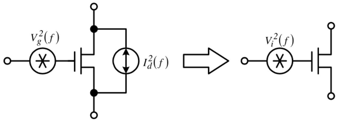
(37) Chapter 3. 3.3.3. Design Considerations for Low-Voltage Low-Power Sigma-Delta Modulator. Thermal Noise. Thermal noise is caused by the thermal motion of the charge carriers in the channel as shown in Figure 3-4. This causes a small amount of random fluctuation in the drain current. Thus, the noise is random at time domain and white in spectrum. Note that the noise voltage has a zero mean value, but a non-zero mean-square value. If the transistor operates in the triode region, as it does for a conducting switch, the noise can be represented by a voltage source in series with the device. The PSD of its voltage is white and can be given by. S vt ( f ) = 4 kTRON. (V 2 / Hz ). (3.2). where k is the Boltzmann constant, k = 1.38 × 10 −23 J/K, T is the absolute temperature of the device in degrees Kelvin, and RON is its on-resistance in ohms. For a MOSFET operates in the active region, the thermal noise can be modeled by a current source in parallel with the channel as shown in Figure 3-5. The PSD of the noise current is approximately given by. S it ( f ) =. 8 kTg m 3. (A 2 / Hz ). (3.3). Vn. t Vn. (a). (b). Figure 3-4 (a) Brown motion and (b) thermal noise at time domain.. I d2 ( f ). Figure 3-5 The thermal noise model in a MOSFET.. - 26 -.
(38) Chapter 3. Design Considerations for Low-Voltage Low-Power Sigma-Delta Modulator. Vg2 ( f ). Vi2 ( f ). I d2 ( f ). Figure 3-6 A simplified equivalent model. However, the analysis may be simplified by an equivalent input noise source as shown in Figure 3-6. In the Figure 3-6, it is an equivalent model which includes 2 results in the simplified flicker and thermal noise. The (3.3) divides by g m. MOSFET model. Hence, the PSD of an equivalent input noise is calculated as. S eq ( f ) =. 8 1 K kT + 3 g m WLC ox f. (3.4). The above equation and model will be used to analyze the impact of noise on a sigma-delta modulator.. 3.4. Power Dissipation of Integrators. 3.4.1. Introduction to Power Dissipation of Integrators. This section describes three architectures of integrators, switched-capacitor, continuous-time, and switched-current. It discusses the suitable architecture for a low-power sigma-delta modulator in terms of power efficiency. The power efficiency is based on the relationship between power and SNR. Since the thermal noise power is usually larger than flicker noise power and quantization noise is dominated by the architecture of sigma-delta modulator, the noise power is only considered thermal noise in this section.. 3.4.2. Switched-Capacitor Integrators. The switched-capacitor circuits take advantages of the linear, well-matched capacitors available in CMOS technologies [14]. The OP amp together with the switches which are provided by MOS transistors make it possible to accurately transfer charges between capacitors. The power consumption in a switched-capacitor - 27 -.
(39) Chapter 3. Design Considerations for Low-Voltage Low-Power Sigma-Delta Modulator. φ1. φ2. Cs. Ci. φ1. φ2 Vin Vref. Vout. Vcmi. φ2. φ1. φ1 φ2. Cs. Ci. Figure 3-7 Switched-capacitor integrator. integrator is generally proportional to the loading. Thus, in order to minimize the power dissipation, the smallest capacitor sizes can be calculated to satisfy the SNR requirement. Figure 3-7 shows a fully differential switched-capacitor integrator. In the following equations, it is assumed that the OP amp has infinite bandwidth and gain. Also there are no parasitic capacitances and the only noise in the integrator is from the sampling switches. The noise power within the signal band in the integrator is calculated as Pn =. f B 4 kT 4 kT ⋅ = f s / 2 Cs OSR ⋅ C s. (3.5). If the maximum amplitude of the differential input signal to the modulator is Vs , the power of a full-scale sinusoidal input is. V2 Ps = s 2. (3.6). Thus, the SNR is derived as. P V 2 ⋅ C s ⋅ OSR SNR = s = s Pn 8 kT. (3.7). From (3.7),. Cs =. 8 kT (SNR ). (3.8). (OSR )Vs2 - 28 -.
(40) Chapter 3. Design Considerations for Low-Voltage Low-Power Sigma-Delta Modulator. The average power dissipation in the integrator is P = I ampV DD. (3.9). where I amp is the average amplifier current and V DD is the supply voltage. For a class A amplifier, the quiescent current is also the maximum current that can be delivered to the load. Hence, the quiescent current must be large enough to ensure that the load can be charged quickly enough to accommodate the largest expected output voltage step within the integration period [14]. Thus, I amp =. Ci ∆Vout Ts / 2. (3.10). where ∆Vout is the largest differential step change in the output voltage, Ts is the sampling period, and it is assumed that the integration must be completed in half the clock period. ∆Vout is given by. ∆Vout = (Vs + Vref. ) CCs. (3.11). i. where Vref is the amplitude of the differential feedback reference voltage of the modulator. By substituting (3.11) into (3.10), I amp can be rewritten as. I amp =. (. ). C s Vs + Vref Ci ∆Vout = 1 / (2 f s ) 1 / (2 ⋅ 2 ⋅ f B ⋅ OSR ). (. = 4C s f B (OSR ) Vs + Vref. ). (3.12). From (3.8), (3.9) and (3.12), the power dissipation in the integrator is given by. P = 32 kT (SNR ) f B. (. V DD Vs + Vref. ). Vs2. (3.13). If Vs = Vref = V DD , the above equation can be simplified as P = 64 kT (SNR ) f B. (3.14). For a class B amplifier, the quiescent power consumption is zero but the power is dissipated at output voltage changes. The average power dissipation of a fully differential integrator implemented with a class B amplifier is [15]. P=. 1 Ci f sV DD ∆Vout 2. (3.15). where ∆Vout is the average differential output voltage step size, which can be given by - 29 -.
(41) Chapter 3. Design Considerations for Low-Voltage Low-Power Sigma-Delta Modulator. ∆Vout =. Cs ⋅ ∆Vin Ci. (3.16). where ∆Vin is the average input voltage of the integrator. Substituting (3.8) and (3.16) into (3.15) results in. P = 8 kT (SNR ) f B. ∆VinV DD Vs2. (3.17). If Vs = V DD , the above equation can be simplified as. P = 8 kT (SNR ) f B. ∆Vin. (3.18). V DD. The above equation and (3.14) indicate that the minimum power dissipation in the first integrator stage of the modulator relate to SNR. Also, the class A amplifier has larger power consumption than class B amplifier. However, the above analysis is assumed that the OP amp is ideal regardless class A or B amplifier. In real cases, the linearity of class B amplifier is not as good. Thus, in order to balance power dissipation and performance, the class AB amplifier is used to implement the integrators. The relationship of power and SNR in class AB amplifier is almost identical to class B. The only difference is that the class AB has quiescent current and this quiescent current is usually much smaller than the peak load current. Thus, the relationship of power and SNR in the class AB amplifier is between class A and class B amplifiers.. 3.4.3. Continuous-Time Integrators. An alternative to the switched-capacitor approach to realizing an integrator is a continuous-time integrator. Figure 3-8 shows a continuous-time integrator. The resistor noise power in the continuous-time integrator with two resistors is given by. Pn = (4 kTR ⋅ 2 f B ) × 2 = 16 kTRf B. (3.19). The SNR can be derived as. P Vs2 SNR = s = Pn 32 kTRf B. (3.20). Vs2 R= 32kTf B (SNR ). (3.21). From (3.20),. - 30 -.
(42) Chapter 3. Design Considerations for Low-Voltage Low-Power Sigma-Delta Modulator. Ci. R. Vin. G f Vref. Vout. R. Ci. Figure 3-8 Continuous-time integrator. Following the method in Section 3.4.2, the minimum power dissipation for the class A amplifier can be estimated as V P = 64 kTf B (SNR ) DD Vs. (3.22). Also, the power dissipation for class B amplifier is derived as. V ∆V P = 32kTf B (SNR ) DD in Vs2. (3.23). For the continuous-time integrators, the amplifier settling requirements are generally more relaxed than switched-capacitor integrators since charge transfer takes place uniformly over the entire clock period [14]. However, the continuous-time integrators are sensitive to timing jitter and hysteresis in the feedback reference signal. Besides, it needs either off-chip resistors or highly linear on-chip resistors. Due to these implementation difficulties, the continuous-time integrator is not very popular.. 3.4.4. Switched-Current Integrators. The switched-current integrator is another alternative to the switched-capacitor approach. The advantage of switched-current integrator is that it does not need linear capacitors and might be attractive for low-voltage system. Figure 3-9 shows a simple switched-current integrator. In the following analysis, the MOS transistors are viewed as square-law devices with infinite output resistance, and the switches are modeled as ideal switches in series with a resistor. The noise power within the signal band in the. - 31 -.
(43) Chapter 3. Design Considerations for Low-Voltage Low-Power Sigma-Delta Modulator. VDD. VDD. 2 I1. φ1. I1. φ1. I out. φ2. I in. M3. M1 M2 C gs1. C gs 2. C gs 3. Figure 3-9 Switched-current integrator. drain current of M1 is calculated as. f kT kT 2 Pn ,M 1 = B ⋅ × gm 1 = f s / 2 C gs1 OSR ⋅ C gs1. ⎛ 2I1 ×⎜ ⎜ V gs − Vth ⎝. ⎞ ⎟ ⎟ ⎠. 2. (3.24). If there are only two settling time constants during the sampling interval (rising edge and falling edge), the duration of the sampling phase is. (. C gs1 C gs1 V gs1 − Vth Ts = 2⋅ = 2 g m1 I1. ). (3.25). From (3.25),. C gs1 =. Ts I 1 2 V gs1 − Vth. (. ). (3.26). Substituting (3.26) into (3.24) results in. Pn ,M 1 = 16 kTf B. I1 V gs1 − Vth. (. ). (3.27). Figure 3-9 includes the drain current noise of M2 in addition to that of M1. The noise in the drain current of M3 is spectrally shaped and is therefore ignored here [14]. Hence, the noise power is approximately twice and can be derived as. Pn = 32 kTf B. I1 V gs − Vth. (. ). (3.28). The power of the integrator input current signal is. I2 Ps = in 2. (3.29). where I in is the amplitude of a full-scale sinusoidal input to the modulator. When. - 32 -.
(44) Chapter 3. Design Considerations for Low-Voltage Low-Power Sigma-Delta Modulator. I in << I 1 , it follows square-law model of an MOS transistor and can be approximated as. I in ≈. 2I1 Vin V gs − Vth. (. ). (3.30). where Vin is the amplitude of the voltage swing at the gate of M1. Substituting (3.30) into (3.29) results in Ps =. 2 I 12Vin2. (3.31). (Vgs − Vth )2. From (3.28) and (3.31), the SNR can be calculated as P I 1Vin2 SNR = s = Pn 16 kTf B V gs − Vth. (. ). (3.32). From (3.32),. I 1 = 16 kTf B (SNR ). V gs − Vth. (3.33). Vin2. The power dissipation of the switched-current integrator in the Figure 3-9 is. P = 3 I 1V DD = 48 kTf B (SNR ). (Vgs − Vth )VDD Vin2. (3.34). From (3.34), (3.14) and (3.18), it can be found that the switched-capacitor integrator has a better power efficiency than a switched-current integrator. Moreover, since Vin is smaller than V DD , the power efficiency will be degraded. Also, it is difficult to achieve high linearity in a switched-current integrator when operating at a low supply voltage.. 3.5. Low-Voltage Switch Techniques. 3.5.1. The Problem of Low-Voltage Switches. Capacitor properties are not strongly affected by supply voltage reduction. It is difficult to properly operate the MOS switches at a low supply voltage [16]. The overdrive voltage of MOS transistor is lowered for a classical transmission gate with the supply voltage reduction. The switch conductance for different input voltages changes depending on the supply voltage as shown in Figure 3-10. In Figure 3-10 (a),. - 33 -.
(45) Chapter 3. Design Considerations for Low-Voltage Low-Power Sigma-Delta Modulator. g ds. g ds. NMOS. g ds min. g ds min SWING. Vov Vthp. Vdd − Vthn. Vov Vdd. Vov Vin. PMOS. SWING. PMOS. SWING. NMOS. Vov Vdd − Vthn. (a). Vthp. Vdd. Vin. (b). Figure 3-10 Transmission gate conductance at (a) standard and (b) low supply voltage.. (a) Vdd = 1.8V. (b) Vdd = 1.0V. Figure 3-11 Switch conductance using TSMC CMOS 0.18 µm process.. when supply voltage is the standard voltage, it is conducting around V DD / 2 . In Figure 3-10 (b), however, there is a critical voltage region around V DD / 2 such that the switch is not conducting. Figure 3-11 shows that the simulation results of a transmission gate at Vdd = 1.8V and Vdd = 1.0V using TSMC CMOS 0.18 µm process. It is obvious that when supply voltage is 1v, it is almost not conducting around V DD / 2 . Hence, it must be operated at proper voltage or by alternative approach such that the switch is conducting. In this section, there are four approaches being pointed out when the supply voltage is low voltage.. 3.5.2. Low-Threshold Voltage. Low-threshold voltage is a necessity for low supply voltage. There are two ways to obtain low threshold voltage MOS transistors. One is to use multi-threshold process. The series connection of low threshold voltage devices shows relatively good conductance and low leakage current as shown in Figure 3-12 [12]. However, this. - 34 -.
(46) Chapter 3. Design Considerations for Low-Voltage Low-Power Sigma-Delta Modulator. φ. Low Vt. φ. Figure 3-12 A composite switch with low threshold voltage. kind of solution has the expense of extra mask steps and higher cost. Another way is to use circuit techniques to reduce the threshold voltage. The threshold voltage is given by Q Vth = φGB − ox + 2φ F + γ C ox. 2φ F − V BS. (3.35). The above equation shows that Vth depends on V BS . The bulk to source junction is reverse biased and causes a threshold voltage increase due to the body effect. If the body effect is reversed, the threshold voltage will be decreased. It is difficult to overcome the problem of the current leakage using low threshold voltage when switch is off. When switch is in off-state, i.e. the weak inversion, the drain current is ⎛ ⎜V ⎛ V gs ⎞ ⎟ = I 0 exp⎜ gs I D = I 0 exp⎜⎜ ⎟ ⎜ kT ⎝ nVth ⎠ ⎜n ⎝ q. ⎞ ⎟ ⎟ ⎟ ⎟ ⎠. (3.36). From (3.36), it is obvious that there is leakage current when the threshold voltage is reduced. This leakage limits the resolution of switched-capacitor circuits due to the break of the charge conservation function.. 3.5.3. Voltage Multiplier. In order to guarantee an adequately low switch resistance in a low voltage environment, the clock voltage used to drive at least one of the two switch transistors can be bootstrapped beyond the supply voltage range. Therefore, voltage multiplier technique is implemented. It converts available voltage to a higher voltage. Figure 3-13 shows a voltage boosted clock driver. C1 and C 2 are charged to V DD via the cross-coupled NMOS M1 and M2. When the input clock, CK, goes high, the - 35 -.
(47) Chapter 3. Design Considerations for Low-Voltage Low-Power Sigma-Delta Modulator. Vdd M1. M2. Vbulk CK sw. C2. C1. M3. CK. Figure 3-13 Voltage boosted clock driver.. Vdd. Vbulk. CK. Figure 3-14 Voltage doubler. output voltage, CK sw , approaches 2V DD . The output voltage does not actually reach 2V DD due to charge sharing with parasitic capacitances. C 2 must be large enough to boost the gates of many MOS transistors to reduce the impact of charge sharing. To decrease the potential for latch-up, the bulk of the PMOS M3 is tied to an on-chip voltage doubler. The bulk of the PMOS switch is biased by the circuit shown in Figure 3-14 [17].. 3.5.4. Clock Bootstrapped Switch. Figure 3-15 shows the clock bootstrapped switch composed of a capacitor, a NMOS switch, and several switches. In the phase φ 2 , the capacitor is pre-charged to V DD and the signal switch is turned off as the gate of switch is connected to VSS .. While in φ 1 , the gate of signal switch is V DD + Vin such that the signal switch provides a constant conductance. Hence, it can handle the rail-to-rail input signal.. - 36 -.
(48) Chapter 3. Design Considerations for Low-Voltage Low-Power Sigma-Delta Modulator. VDD. VSS S3 φ 2. φ 2 S4 Coffset. S1 φ 1. φ1. S2 S5 φ2. Vin. VSS. N-switch. Figure 3-15 The architecture of clock bootstrapped switch. Figure 3-16 shows the real transistor-level implementation of the switch bootstrapping circuit. Transistors MN1, MP1, MN2, MP2, and MN4 correspond to the five ideal switches S1-S5 respectively. MN3S triggers MP1 at the beginning of φ 1 while MN3. VDD. φ2. MN2. MP2. φ2 MP3. A. Coffset. φ1 MN3S. MP1 VDD. MN3. MN4. MN1 Vin. φ2. MNT4 N-switch. Figure 3-16 Transistor-level implementation of bootstrapped switch.. - 37 -. Vout.
(49) Chapter 3. Design Considerations for Low-Voltage Low-Power Sigma-Delta Modulator. keeps it on as the voltage on node A rises to Vin . MNT4 has been added to prevent the gate-drain of MN4 from exceeding V DD during φ 1 while it is off [18].. 3.5.5. Switched Opamp Technique. Figure 3-17 shows a classic non-inverting integrator. For switch driving problem, the switches in Figure 3-17 can be classified into two types. One is that the switches having one channel terminal connected to the level of reference voltage (S2 and S3) or virtual ground (S4). Another is that the switch is not connected to ground but to a signal source (S1). The first type of switches can always be turned on if the switch driving voltage is at least a threshold voltage above its source which is at ground level. However, the second type of switches needs to be switched over the entire signal range. Therefore, the switched opamp technique can be used to replace this critical switch as shown in Figure 3-18. In phase φ 1 , the opamp is turned off and samples C2. C1. S1 φ1. S4 φ2 Vout. φ 2 S2. Vin. φ 1 S3. Figure 3-17. Non-inverting integrator.. S1 C2 C1. S4. φ2 Vin. φ1. φ2 φ1. φ2 S2. φ1 S3. Figure 3-18 The switched opamp principle.. - 38 -. Vout. φ2.
(50) Chapter 3. Design Considerations for Low-Voltage Low-Power Sigma-Delta Modulator. signal from the output of opamp inside the dotted box. In phase φ 2 , the opamp is turned on to transfer charge to the output. However, this approach introduces extra active elements such that the chip area is increased. Fortunately, the power consumption is not affected since these opamps are turned on half of the period [19].. 3.6. Summary. There are many details to take care in the design of a low-voltage, low-power sigma-delta modulator. The low-voltage system is sensitive to the noise interference. The quantization noise is dominated by noise transfer function. The thermal noise can be reduced by increasing capacitance. The switched-capacitor integrator is a better architecture to implement a sigma-delta modulator. It has higher power efficiency and can be easily realized in practical circuits. Also, the switch driving problem is an important issue in a low voltage system. Several techniques used to solve low supply voltage switched-capacitor integrator, such as low threshold process, voltage multiplier, clock bootstrapped switch, and switched opamp. In the following section, the voltage multiplier will be used as the basic components to implement the sigma-delta modulator.. - 39 -.
數據

![Figure 2-10 shows the architecture of a first-order sigma-delta modulator. To realize first-order noise-shaping, the noise transfer function, N TF ( )z , should have a zero at dc (i.e., z=1) so it is high pass for the quantization noise [1]](https://thumb-ap.123doks.com/thumbv2/9libinfo/8465512.183334/24.892.140.768.431.1072/figure-architecture-modulator-realize-shaping-transfer-function-quantization.webp)
+7
![Figure 3-9 includes the drain current noise of M2 in addition to that of M1. The noise in the drain current of M3 is spectrally shaped and is therefore ignored here [14]](https://thumb-ap.123doks.com/thumbv2/9libinfo/8465512.183334/43.892.136.756.111.341/figure-includes-current-addition-current-spectrally-shaped-ignored.webp)

相關文件
專案執 行團隊
Digital PCR works by partitioning a sample into many individual real-time PCR reactions, some portion of these reactions contain the target molecules(positive) while others do
首先,在前言對於為什麼要進行此項研究,動機為何?製程的選擇是基於
Robinson Crusoe is an Englishman from the 1) t_______ of York in the seventeenth century, the youngest son of a merchant of German origin. This trip is financially successful,
Courtesy: Ned Wright’s Cosmology Page Burles, Nolette & Turner, 1999?. Total Mass Density
In this study, we compute the band structures for three types of photonic structures. The first one is a modified simple cubic lattice consisting of dielectric spheres on the
由圖可以知道,在低電阻時 OP 的 voltage noise 比電阻的 thermal noise 大,而且很接近電阻的 current noise,所以在電阻小於 1K 歐姆時不適合量測,在當電阻在 10K
• Definition: A max tree is a tree in which the key v alue in each node is no smaller (larger) than the k ey values in its children (if any). • Definition: A max heap is a
