國
立
交
通
大
學
光電學院光電科技學程
碩
士
論
文
使用 SMT 表面黏著技術評估銅柱凸塊覆晶元件封裝之研究
Study of Surface Mount Technology on
Copper Pillar Bump Flip-Chip Package
研 究 生:許翰誠
指導教授:林建中 副教授
使用 SMT 表面黏著技術評估銅柱凸塊覆晶元件封裝之研究
Study of Surface Mount Technology on
Copper Pillar Bump Flip-Chip Package
研 究 生:許翰誠 Student:Han-Cheng Hsu
指導教授:林建中 Advisor:Chien-Chung Lin
國 立 交 通 大 學
光 電 科 技 學 程
碩 士 論 文
A ThesisSubmitted to Degree Program of Photonic Technology College of Photonics
National Chiao Tung University in partial Fulfillment of the Requirements
for the Degree of Master
In
Photonic Technology
July 2013
Tainan, Taiwan, Republic of China
-I-
使用 SMT 表面黏著技術評估銅柱凸塊覆晶元件封裝之研究
學生:許翰誠
指導教授:林建中
國立交通大學 光電科技學程碩士班
摘
要
覆晶封裝技術是指在晶圓上完成凸塊製程後將晶圓切割成單顆晶粒,
再透過覆晶銲接機將晶粒與 IC 載板進行接合,之後透過迴銲製程完成封裝
元件的固定。此新的封裝型態符合電子元件市場上的高功能、高可靠度和
低價位的技術需求。早期凸塊製程是以錫鉛凸塊或是錫銀銅凸塊為主,但
隨著晶圓製程的微縮,晶粒尺寸的縮小,錫鉛凸塊或是錫銀銅凸塊已無法
符合新一代技術需求,因此,能符合小間距的銅柱凸塊漸漸獲得重視。
為增加覆晶製程的彈性配置以及與系統化構件(SIP)、2.5D IC…等新
型態封裝構件快速整合的作業需求,本研究評估使用表面黏著技術在相同
銅柱凸塊覆晶條件下,搭配不同成份之錫膏、導線架材料將晶粒與 IC 載板
進行接合並預期逹到高可靠度的需求。透過銲接製程參數的調整、最佳化
後進行可靠度與加速壽命試驗。將測試結果分析確認符合韋布分布後計算
-II-
出相關參數並使用 Arrhenius relationship 公式預測產品使用壽命。
研究發現搭配表面黏著技術搭配三種不同成份的錫膏-① 錫 96.5%/銀
3%銅/0.5%、② 錫 97%/銀 3%/與 ③ 錫 95.5%/銀 4%/銅 0.5% ,在純銅表面
處理的導線架基板上可以達到 10 年以上的使用壽命並符合電子元件在可靠
性上的需求,其中,以相同製程搭配錫 95.5%/銀 4%/銅 0.5% 的錫膏可以得
到最好的可靠性結果。
-III-
Study of Surface Mount Technology on
Copper Pillar Bump Flip-Chip Package
Student: Han-Cheng Hsu
Advisors: Dr. Chien-Chung Lin
Degree Program of Photonic Technology
National Chiao Tung University
ABSTRACT
Flip chip assembly technology means to deposit bumps on the chip pads on
the topside of a wafer, the second step is to saw the wafer into chip units and use
flip chip bonder to mount chips on carriers like substrates or lead frames. The
final step is to use IR reflow oven to firm the package. Solder bump technology
has been developed in the beginning of flip chip package technology and has
high volume production today, but now the copper pillar bump trends up due to
the process limit of solder bump.
To meet the high flexible operation in flip chip process and integrate with
other packages such as System in Package (SiP), 2.5D IC…etc, we investigate
surface mount technology (SMT) and daisy-chain chip with copper pillar bump
in this study. The materials are also considered for different components of
solder paste and lead frame surface treatment. After process optimization, the
samples proceed reliability test and Accelerated Lifetime Test (AL). After
-IV-
confirmed the data can meet Weibull distribution, we use Arrhenius relationship
equation to predict the use lifetime.
Finally, we found the SMT process with 3 types of solder pastes (Sn 96.5%/
Ag 3%/ Cu 0.5%, Sn 97%/ Ag 3%, Sn 95.5%/ Ag 4%/ Cu 0.5%) and pure
copper treatment on lead frame surface can reach use lifetime and high
reliability requirement for ten years, the best result for the reliability
performance is the same process with Sn 95.5%/ Ag 4%/ Cu 0.5% solder paste.
-V-
誌 謝 Acknowledgement
當初一聽到光電學院要開在職專班時,就下定決心要來這兒進修,經過
一番比試,果然也順利進到這兒與來自四面八方的英雄好漢齊聚一堂,努
力精進學問。
就學期間,除了承蒙課堂上諸位良師教導之外最感恩的是指導教授林建
中教授,一路上義氣相挺,悉心指導,在研究主題上給學生很大的發展空
間,在研究方法上也不吝將拿手絕技傾囊相授,適時提點,讓學生功力大
進,此外,平易近人的教授更常將之前的經驗、產業現況與當前學術研究
趨勢與學生分享,讓學生思路大開,也得以在學術之海更清晰的遨遊。
另外要感謝的是南茂科技公司對學生的研究全力支持,在材料準備、製
程檢驗、作業機台及可靠度測試設備的提供等,都能盡力滿足學生的需求,
使學生的研究得以順利完成。
有家人的支持,這個結果才別具意義。在此也要感謝我的牽手淑貞,在
學生忙碌於事業與學業間分身乏術之時,這期間家中恰巧發生了許許多多
的事情,而她總能夠一一化解,不但照顧好家中的老老少少,包含二個可
愛的小搗蛋-潪銘與縈熒,也將這些突如期來的事情處理得順遂圓融,果真
是一位賢內助。
最後要將這份論文獻給在西方的母親,雖然她無緣親眼見到她的寶貝兒子
在學業上又更進一步,但相信這份榮耀她可以感應得到。
-VI-
Table of Contents
Chinese Abstract
………
i
English Abstract
………
iii
Acknowledgement
………
v
Table of Contents
………
vi
List of Tables
………
viii
List of Figures
………
ix
List of Abbreviations
………
xii
List of Symbols
………
xiii
I.
Introduction………
1
1.1
The trend chart on the IC package market ………
1
1.2
Flip chip package………
2
1.2.1
Assembly process of Flip chip package ………
3
1.3
Surface-mount technology (SMT) ………
8
II.
Motivation and Theory………
9
2.1
Motivation………
9
2.2
Theory ………
12
2.2.1
The Bath-tube curve model ………
12
2.2.2
Weibull distribution ………
14
2.2.3
Arrhenius relationship equation………
19
2.3
Reliability test ………
20
2.3.1
Environment test ………
21
2.3.2
Stress test ………
22
III.
Evaluation plan and procedure………
25
3.1
Evaluation plan………
25
3.1.1
Fixed materials on the design of experiments (DoE) …
26
3.1.2
Key factor materials on the design of experiments (DoE)
29
3.1.3
Design of experiments (DoE) matrix………
31
3.2
Examination items for process check ………
32
3.3
Process optimization………
36
3.4
Test sample manufacturing ………
42
3.4.1
The assembly process flow ………
42
3.4.2
Quality inspection result ………
43
IV.
Evaluation Result Analysis ………
50
-VII-
4.2
Temperature cycling test (TCT) failure distribution……
51
4.3
Weibull distribution ………
52
4.3.1
Weibull distribution for PCT………
53
4.3.2
Weibull distribution for TCT………
57
4.4
Life time prediction………
61
4.5
Failure mode analysis………
63
4.6
Summary………
64
V.
Summary and Future Work………
65
Bibliographies
………
67
Appendix 1
………
69
Appendix 2
………
70
-VIII-
List of Tables
Table. 1-1 Moisture Sensitivity Levels
Table. 2-1 process comparison of flip chip package
Table. 2-2 Moisture Sensitivity Levels
Table. 3-1 The comparison table of solder paste
Table. 3-2 The comparison table of solder paste
Table. 3-3 The full factorial DoE
Table. 3-4 The shearing test result
Table. 3-5 Initial resistance measurement data
Table. 4-1 PCT test result
Table. 4-2 TCT test result
Table. 4-3 Resistance measurement after TCT test
Table. 4-4 Weibull distribution for PCT
Table. 4-5 Weibull distribution for PCT
Table. 4-6 The life time prediction
-IX-
List of Figures
Fig. 1-1 Overall Wafer level packaging demand
Fig. 1-2 Conventional IC package (T/QFP)
Fig. 1-3 The cross-section of Flip chip package
Fig. 1-4 Solder bumps on wafer
Fig. 1-5 Copper pillar on wafer
Fig. 1-6 Illustration of die sawing process
Fig. 1-7 Illustration of die bonding process
Fig. 1-8 IR reflow profile
Fig. 1-9 Under-fill adhesive dispensing process and molding process
Fig. 2-1 The main process flow of flip chip package
Fig. 2-2 The main process flow of flip chip package for SMT method
Fig. 2-3 The Bath-tube curve model
Fig. 2-3 The Bath-tube curve model
Fig. 2-4 The reliability function for lifetime and failure rate
Fig. 2-5 The PDF shapes of the Weibull distribution
Fig. 2-6 the value of β on the Weibull failure rate Fig. 2-7 the value of η on the Weibull failure rate Fig. 3-1 Evaluation procedure
Fig. 3-2 Cross-section view of flip chip CSP package
Fig. 3-3 Cross-section view of a copper pillar bump
Fig. 3-4 Top view of chip with daisy-chain design
Fig. 3-5 The bumping process flow
Fig. 3-6 Solder paste
-X-
Fig. 3-8 The die shear testing method
Fig. 3-9 The HP-34970A Ohmic testing equipment
Fig. 3-10 Hitachi Temperature cycling test oven
Fig. 3-11 HIRAYAMA Pressure cooker
Fig. 3-12 Fuji NXP chip place machine
Fig. 3-13 BTU IRreflow oven
Fig. 3-14 Solder paste printing process
Fig. 3-15 IR-reflow profile
Fig. 3-16 Solder plating on copper leadframe
Fig. 3-17 Appearance check result of solder paste printing by different stencil opening
Fig. 3-18 Abnormal photo for insufficient solder
Fig. 3-19 FC CSP process flow
Fig. 3-20 The appearance inspection
Fig. 3-21 The appearance inspection after molding process
Fig. 3-22 Die shearing test analysis
Fig. 3-23 The breaking mode after die shearing test
Fig. 3-24 The X-ray inspection for a defect unit
Fig. 3-25 The X-ray inspection for normal units
Fig. 3-26 CSAM inspection result
Fig. 3-27 Cross-section
Fig. 4-1 Weibull distribution for PCT Cell-1
Fig. 4-2 Weibull distribution for PCT Cell-2
Fig. 4-3 Weibull distribution for PCT Cell-3
Fig. 4-4 Weibull distribution for PCT Cell-4
-XI-
Fig. 4-6 Weibull distribution for PCT Cell-6
Fig. 4-7 Weibull distribution for TCT Cell-1
Fig. 4-8 Weibull distribution for TCT Cell-2
Fig. 4-9 Weibull distribution for TCT Cell-3
Fig. 4-10 Weibull distribution for TCT Cell-4
Fig. 4-11 Weibull distribution for TCT Cell-5
Fig. 4-12 Weibull distribution for TCT Cell-6
-XII-
List of Abbreviations
SIP
: System in Package
POP
:
Package on PackageSMT
: Surface mount technology
TQFP
: Thin quad-flat package
JEDEC : Join electron Device Engineering Council
AL
: Accelerated lifetime test
MUF
: Molding under fill
C4
: Controlled collapse chip connection
AOI
: Automatic Optical Inspection
FEM
: Finite Element Method
: Probability density function
RDL
: Redistribution layer
MSL
: Moisture Sensitivity Level
CSP
: Chip scale package
CTE
: Coefficient of Thermal Expansion
CSAM
: Scanning Acoustic Microscopy
PCT
: Pressure cooker test
TCT
: Temperature cycling test
PPF
: Pre-plated leadframe
-XIII-
List of Symbols
F(x)
: the failure function
ƒ(x)
: the failure probability density function
t
: the length of the period of time
h
: constant failure rate
β
: shape parameter (or slope)
η
: characteristic life time or scale parameter
γ
: location parameter.
R
:
reaction rate
K
: Boltzmann’s constant (8.617×10⁻⁵ ev/k )
AF
: acceleration factor
T
L: low temperature
T
H: high temperature
Luse
. :
lifetime during normal use
Laccl
: lifetime during acceleration use
RH.: humidity
n.
: integer constant from 1 to 7
Ttest.
:
temperature during test ( [K] = 273 +temperature in ˚C) Tuse.:
temperature during use-1-
Chap 1. Introduction
The demands of 3C products in consumer market, especially for portable devices like
smart phones and tablets have been highly grown in recent years. New products with light,
slim and portable characters are changing human’s work way and life style today, as well as
the communication method.
As following the demands from the market, the electronic devices trends to high speed,
multi-function, low power consumption and large capacity integration. The conventional
assembly packages slows down and new packages to meet this market trend are widely
developed, like Flip chip package, Chip scale package (CSP), System in package (SiP),
Package on Package (PoP), 2.5D IC, 3D IC, WLCSP...etc.
1-1 The trend chart on the IC package market
Following the evolution of semiconductor technology, the volume and transistors density
of Integrated Circuit (IC) device is increasing. The popularly known as Moore's Law, which
was described by Intel co-founder Gordon E. Moore in his 1965 paper, states that the number
of transistors on a chip will double approximately every two years. Now this rule is still
working even over 4 decades.
For the demand from the market view, the IC package size trends to become smaller, in
addition, with more function, higher reliability performance and lower cost are also strongly
-2-
Fig. 1-1 Overall Wafer level packaging demand
(Source: Equipment & Materials for 3DIC and Wafer-Level-Packaging (Yole),2011)
From the combo of wafer level package, the major portion is flip chip package, because it
can meet all the requirements in today’s market and for other combo packages, it will grow 20
percent per year in the future.
1.2 Flip chip package
Flip chip technology is a way to connect different types of electronic components directly
by using conductive solder bumps instead of wires.
The traditional technology is to mount the chip face-up on the leadframe or substrate, and
bond gold wires from alumina pad of the chip to the lead land for circuit connection, then
molding capsulation process is performed as Figure 1-2, the conventional IC package.
-3-
No bonding wire is needed on flip chip technology, it replaces wire bonding process and
allows integrated circuit chips to be directly connected with external circuits through
conductive bumps present on the chip's surface. A direct chip-attach or controlled collapse
chip connection (C4) is also called. This process becomes very popular and large resources
are invested because it reduces packaging size and offers better electrical performance.[1] The
Figure 1-3 shows the cross- sectioning of flip chip package.
Fig. 1-3 The cross-sectioning of flip chip package
(Source: http://www.faraday-tech.com/html/Product/ASICService/Package/FlipChip.htm)
1-2-1 Assembly process of Flip chip package
The assembly process is to place the bump onto the chip pads on the topside of the wafer,
the second step is to saw the wafer to chip unit and use flip chip bonder to mount the chip on
substrate. The final step is to use IR reflow oven to firm the package and isolate the chip by
epoxy, the below lists the detail process.
1. Wafer bumping process
The wafer bumping process is to deposit the bump onto the alumina pads of chip on
the topside of the wafer during the final wafer process, the below Figure 1-4 and Figure
-4-
Fig. 1-4 Solder bumps on wafer
Fig. 1-5 Copper pillar bumps on wafer
There are two types of bumps well used in the flip chip package: solder bump and
copper pillar bump. Solder bump is popular and highly manufactured, because this
material is evaluated and introduced to mass production from the beginning of package
development. But the situation is changed now due to the copper pillar bumps has
below advantages:
a. Better electrical performance than the conventional solder bump for high power
application devices.
b. The diameter of copper pillar bump is smaller than solder bump and can be used on
high density or high pin count devices.
-5-
since 2010.
The base band platform - OMAP 4430 from Texas Instruments (TI) applied on
Amazon Kindle Fire tablet and Motorola Droid X cell phone are also used copper pillar
bump on flip chip technology.
Considering to the view of package cost, the major communication chip design house,
like Qualcomm, Marvell, Broadcom, Infineon, Mediatek all follow this trend to develop
flip chip with copper pillar bump. So based on the prediction by market research
institute, the market share will be 30 % ata least in 2015.
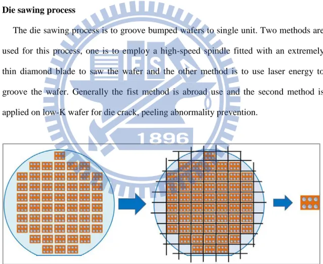
2. Die sawing process
The die sawing process is to groove bumped wafers to single unit. Two methods are
used for this process, one is to employ a high-speed spindle fitted with an extremely
thin diamond blade to saw the wafer and the other method is to use laser energy to
groove the wafer. Generally the fist method is abroad use and the second method is
applied on low-K wafer for die crack, peeling abnormality prevention.
Fig. 1-6 Illustration of die sawing process
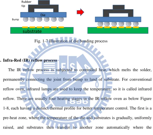
3. Die bonding process
-6-
connection purpose. The rubber tip with vacuum is used to pick up the chip from the
wafer and flip the die 180°. The die is attached on the substrate with precisely alignment
the bump position to the topside land on the substrate.
Fig. 1-7 Illustration of die bonding process
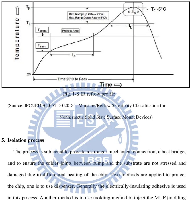
4. Infra-Red (IR) reflow process
The IR reflow process is subjected to controlled heat, which melts the solder,
permanently connecting the joint from bump to land of substrate. For conventional
reflow oven, infrared lamps are used to keep the temperature, so it is called infrared
reflow. There are usually four heating stages in the IR reflow oven as below Figure
1-8, each having a distinct thermal profile for better temperature control. The first is a
pre-heat zone, where the temperature of the die and substrates is gradually, uniformly
raised, and substrates then transfer to another zone automatically where the
temperature is high enough to melt the solder, uniformly cooling down is the next to
prevent the damage on package from the stress of temperature change.
Die
substrate
BumpRubber tip
-7-
Fig. 1-8 IR reflow profile
(Source: IPC/JEDEC J-STD-020D.1, Moisture/Reflow Sensitivity Classification for Nonhermetic Solid State Surface Mount Devices)
5. Isolation process
The process is subjected to provide a stronger mechanical connection, a heat bridge,
and to ensure the solder joints between bump and the substrate are not stressed and
damaged due to differential heating of the chip. Two methods are applied to protect
the chip, one is to use dispenser. Generally the electrically-insulating adhesive is used
in this process. Another method is to use molding method to inject the MUF (molding
underfill) into the package.
Fig. 1-9 Under-fill adhesive dispensing process and molding process
adhesive
Molding under-fill Epoxy Dispenser
-8-
1-3 Surface-mount technology (SMT)
The surface-mount technology is a method for making electronic circuits in which the
components are placed directly onto the surface of substrate or printed circuit boards (PCBs).
After IR relow or wave reflow process, the components are connected. This process was
developed in the 1960s and became widely used in the late 1980s.
The first step is to print the solder paste on the substrate. Solder paste, a sticky mixture of
flux and tiny solder particles, is applied to pads of substrate or PCBs with a stainless steel
stencil using a screen printing process. It can also be applied by a jet-printing mechanism for
fine pitch devices. After finished printing process, the substrate proceeds to the
pick-and-place machines. The components are placed on the substrate by rubber tip with
vacuum. Then the substrate is inspected by an Automatic Optical Inspection (AOI) to make
sure all the components are at the correct position. Next, the substrate transfers into the IR
reflow oven.
The surface tension of the molten solder helps keep the components in place, and if the
solder pad geometries are correctly designed, surface tension automatically aligns the
components on their pads.
After IR-reflow process, AOI is applied again to inspect all components are well to place
-9-
Chap 2. Motivation and Theory
2-1 Motivation
For the high demand on mobile and tablet portable products, the package size of Integrate
circuit devices (IC) trends to get thin and small. The saved space is designed to enlarge the
cell capacity. This purpose is to reach longer standby and operation time on 3C products.
Chip scale package (CSP) is developed in this intension, so we will focus on chip scale
package with copper pillar bump in this study. Moreover, it also can be extended to the
application of System in Package (SiP). SiP is a number of integrated circuits enclosed in a
single package. They are connected internally by bonding wires or with a flip chip assembly,
solder bumps to join the circuit.
The major process for flip chip package is to use die bonder to mount the chip with copper
bumps on substrate/ lead frame, as below figure. Through this method, only Sn/Pb bump or
Cu/Sn bump can be applied on this process.
-10-
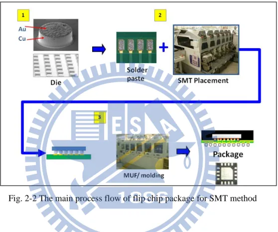
As we mentioned on above paragraph, this study is focused on surface mount technology
to mount chips on lead frame or substrate, a SMT and molding processes are used in this CSP ,
as show in Figure 2-2.
Fig. 2-2 The main process flow of flip chip package for SMT method
Besides the SMT process evaluation, we include solder materials and surface treatment of
lead frame on it. By this way, we plan to extend the machine application from SiP to flip chip
package, also expect to integrate more function on multi packages.
We think this could be a simple way to get good reliability performance through Interfacial
Bonding Behavior between Sn-Ag-Cu Series solder materials and lead frame surface
treatment. Through the join of different solder composition ( Sn/Ag/Cu base) and lead frame
treatment, the intermetalic compound (IMC) is formed between the Cu pillar bump and the
leadframe surface. This intermetalic compound will affect the interfacial bonding strength and
-11-
The below table shows the advantage and disadvantage comparison of both processes of flip
chip package.
Traditional (original) New method
Advantage 1.Mature production process 2.High pint count application 3.High thermal dispatch
1.High reliability performance 2.No need solder cap on bump/ pillar
3.Flexibility for application on other package
Disadvantages 1.Reliability concern on high level 2.Solder cap on bump is needed
1.Limit on high I/O chip application 2.Narrow process window in process
Table. 2-1 process comparison of flip chip package
The weakness point on Flip chip package is the solder joint of copper pillar bump to lead
frame or substrate, there are many papers submitted to use Finite Element Method software
(FEM) for the simulation. A paper issued by Yunn-Horng Guu mentioned the pillar bump
with a copper base and eutectic solder cap had a higher resistance to fatigue failure in
comparison with a pure eutectic solder bump, the mechanical behavior of the flip-chip packag
is a crucial issue in the packaging industry, and it is also related to the reliability of electronic
devices[3].
The solder paste is highly related to the solder join of the bonding interface, refer to the
study result of paper [4] [5], the solder paste with Ag content 3.0% to 4.0 % has below
characters :
1. Better thermal fatigue resistance and reliability result
-12-
3. Broader process window
4. Better Joint reliability compared to non-silver lead-free and tin-lead alloys.
Based on these data, three types of solder paste: Sn 96.5%/ Ag 3%/ Cu 0.5%, Sn 97%/
Ag 3% and Sn 95.5%/ Ag 4%/ Cu 0.5% are chose for this study.
2-2 Theory
The reliability test is used to exam the result of the evaluation on this study.
Reliability is defined as the probability that a device or system will perform its intended
function during a designated period of time under stated conditions.
2-2-1 The Bath-tube curve model
The bathtub curve is used in reliability engineering and is generated by mapping the rate of
early "infant mortality" failures when first introduced, the rate of random failures with
constant failure rate during its "useful life", and finally the rate of "wear out" failures as the
product exceeds its design lifetime. Please refer the below Figure 2-3, the first part is a
decreasing failure rate, known as early failures., the second part is a constant failure rate,
known as random failures and the third part is an increasing failure rate, known as wear-out
-13-
Fig. 2-3 The Bath-tube curve model
The probability of reliability function is as
R(t) = P{T > t} = 1 − P{T ≤ t} = 1 − FT(t), t ≥ 0 (2-1) From (2-1)
𝑓𝑓T(t) = −R′(t) and 1 − R(t) = FT(t) = P{T ≤ t} (2-2) where F(x) is the failure function, and
ƒ(x) is the failure probability density function,
-14-
Fig. 2-4 The reliability function for lifetime and failure rate
h means constant failure rate or can be called hazard rate. It is defined for non repairable populations as the rate of failure for the survivors to time t during the next instant of time, and
the function is as h(t) = lim∆𝑡𝑡→0P(t < T ≤ t + ∆t|T > t) Δt = lim∆𝑡𝑡→0P(t < T ≤ t + ∆t)Δt ∙ P(T > 𝑡𝑡) = lim∆𝑡𝑡→0F(t+∆t)−F(t) Δt ∙ 1 R(t) = F′T(t) 1−FT(t) = 𝑓𝑓T(t) R(t) (2-3)
MTTF is Mean Time To Failures (for non-repairable equipments), and the equation is
MTTF = 1 / h
The cumulative distribution function corresponding to a bathtub curve and may be analyzed
using a Weibull distribution chart.
2-2-2 Weibull distribution
-15-
the Swedish physicist Waloddi Weibull. He used it for modeling the distribution of breaking
strength of materials, now this distribution is applied to model many different failure
distributions.
This distribution can handle increasing, decreasing or constant failure rates. The Weibull
distribution is flexible and fits to a wide range of data, including normal distributed data. Only
Log-Normal data does not fit in the Weibull distribution and needs separate analysis.
For a comprehensive review of applications, we refer the readers to Johnson et al. (1994)
and Murthy et al. (2003)[7]. Given a shape parameter, β, and characteristic life time, η, the three-parameters Weibull distribution probability density function (PDF) and reliability
function are given by:
𝑓𝑓T(t) = β η� t−γ η � β−1 e−�t−γη � β , t ≥ γ (2-4) FT(t) = 1 − e−� t−γ η � β (2-5) where t ≥ 0, β> 0, η> 0, γ> 0 , and
β : shape parameter (or slope)
η: characteristic life time or scale parameter
γ: location parameter.
t = time, cycles, miles, or any appropriate parameter;
Generally, the location parameter is not used and the value can be set to zero, so the PDF
equation can be reduced to two-parameter Weibull distribution.
𝑓𝑓T(t) = β η� t η� β−1 e−�ηt� β , t ≥ γ (2-6)
-16-
Weibull Parameters
The shape parameter, BETA (β) is known as Weibull slope, it shows how the failure rate
develops in time. Different values of the shape parameter can have responded effects on the
behavior of the distribution. Figure 2-5 shows the effect of different values of the shape
parameter, β, on the shape of the PDF (while keeping γ constant), we can see the shape of the PDF can take on a variety of forms based on the value of β.
Fig. 2-5 The PDF shapes of the Weibull distribution
(Source: http://www.weibull.com/hotwire/issue14/relbasics14.htm)
Another characteristic of the distribution where the value of β has a distinct effect is the failure rate. Figure 2-6 shows the effect of the value of β on the Weibull failure rate.
-17-
Fig. 2-6 the value of β on the Weibull failure rate
(Source: http://www.weibull.com/hotwire/issue14/relbasics14.htm)
This is one of the most important aspects of the effect of β on the Weibull distribution. Weibull distributions with β < 1 have a failure rate that decreases with time, also known as infantile or early-life failures. Weibull distributions with β close to or equal to 1 have a fairly constant failure rate, indicative of useful life or random failures. Weibull distributions with
β > 1 have a failure rate that increases with time, also known as wear-out failures. Corresponding to below equation (2-3) and (2-4) , we also can find the failure rate as
h
(t)=
𝑓𝑓T(t) R(t)=
β η�
t−γ η�
β−1 (2-7)-18-
The ETA (η) is characteristic life time or scale parameter, increasing the value of η while holding β constant has the effect of stretching out the PDF. Since the area under a PDF curve is a constant value of one, the "peak" of the PDF curve will also decrease with the increase of
η, as indicated in the following figure.
Fig. 2-7 the value of η on the Weibull failure rate
(Source: http://www.weibull.com/hotwire/issue14/relbasics14.htm)
If η is increased, while β and γ keep the same, this distribution gets stretched out to the right and its height decreases, while maintaining its shape and location.
If η is decreased, while β and γ keep the same, the distribution gets pushed in towards the left, and its height increases.
-19-
2-2-3 Arrhenius relationship equation
The semiconductor and system manufacturers face strong pressure to develop new and
higher reliability products in short term today. The instant time-to-market becomes the
success factor of new product promotion. Accelerated Test (AT) is developed based on this
concept. Refer the readers to Thomas P. Ryan et al. (2007, chapter 14) [8], an accelerated
failure model relates the time-to-failure distribution to the stress level. The general idea is that
the level of stress is only compressing or expanding time and not changing the shape of the
time-to-failure distribution.
With this assumption, changing stress is equivalent to transforming the time scale used to
record the time at which failures occur, so it is a matter of “decelerating” back to normal use
by using an appropriate acceleration factor. This is accomplished by using acceleration
models.
Arrhenius relationship equation is commonly used on the accelerated test for the life time
prediction in normal use condition and environment. It is expected that as stress is increased,
like temperature, humidity, a reaction such as a chemical reaction, will occur more rapidly.
The Arrhenius equation reflects this idea and is named after S. A. Arrhenius (1859–1927).
The equation when applied to accelerated testing is given by
𝐿𝐿(temp) = A ∙ e�𝑘𝑘∙tempK−𝐸𝐸𝐸𝐸 � (2-8)
where L is the reaction rate, A is an unknown non-thermal constant, temp K is temp
C+273.15, is thermodynamic temperature in kelvin (K), k is Boltzmann’s constant
(8.617×10⁻⁵ ev/k ) or the universal gas constant and Ea is the activation energy based on
characteristics of product or material.
-20-
accelerated life test conditions to a failure rate indicative of normal use temperature for
electrical devices. From the equation (2-8), the AF is found
AF = Luse Laccl = A∙e�−𝐸𝐸𝐸𝐸𝑘𝑘∙TL� A∙e� −𝐸𝐸𝐸𝐸𝑘𝑘∙TH �= e Ea k�TL1−TH1� (2-9)
where AF is acceleration factor, Luse is lifetime during normal use, Laccl is lifetime during
acceleration use, TL is low temperature ( [K] = 273 +temperature in ˚C) and
TH is high temperature.
For the relationship about humidity and temperature, from the study by D. Stewart Peck in
1986, an acceleration formula is described which provides direct extrapolation from test
results on humidity and temperature[9], the equation is given
Time to failure (RH)n∙ e�𝑘𝑘∙T𝐸𝐸𝐸𝐸� (2-10) AF = Luse Laccl = � RHtest RHuse� n ∙ e�𝑘𝑘∙T𝐸𝐸𝐸𝐸��ttest1 − tuse1 � (2-11)
where RH is humidity, n is integer constant from 1 to 7, Ttest is temperature during test ( [K]
= 273 +temperature in ˚C) and Tuse is temperature during use.
2-3 Reliability test
The “Reliability” is the ability of a system or component to perform its required functions
under stated conditions for a specified period of time.[10] Reliability is theoretically defined
as the probability of failure, the frequency of failures, or in terms of availability, in other
words, failure rate, average life, mean time to failure (MTTF), etc. From the test data, the
-21-
play an important role in improving reliability by analyzing failures which occur during tests
and clarifying these failure mechanisms. Reliability tests provide the greatest effects when
statistics and failure physics function reciprocally.
2-3-1 Environment test
The environment test is identified the classification level of nonhermetic solid state surface
mount devices (SMDs) that are sensitive to moisture-induced stress so that they can be
properly packaged, stored, and handled to avoid damage during assembly solder reflow
process.
There are eight levels defined for this test and is called Moisture Sensitivity Level (MSL),
as shown in Table 2-2. This standard is used to determine what classification or
preconditioning level should be used for SMD package qualification.[11]
Table. 2-2 Moisture Sensitivity Levels
-22-
appropriate electrical testing and acoustic microscope, if one or more devices are failed, the
package shall be considered to have failed the test and stop to go to next stress test.
2-3-2 Stress test
The purpose of stress test is to precipitate failures in an accelerated manner compared to
normal use conditions. Test units are subjected to higher than usual levels of one or more
accelerating variables such as temperature, humidity, voltage and current. Then the test results
are used to analysis packaging failures or predict life of the units at use conditions. Anand
model[12] was employed to represent the constitutive equation of solders in stress model and
developed to life prediction model in the accelerated thermal test. [13]
There are many industry-standard package-level reliability tests. The test is chosen based
on the failure mechanism, as different stress tests accelerate different failure mechanisms. It is
also important to select test methods which are as standardized as possible in consideration of
test reproducibility, cost effectiveness, data compatibility and other factors [14]. These tests
are described as below.
1. Biased Highly Accelerated Stress Test (HAST) (JESD22-A110)
The purpose is to simulate extreme operating conditions. Devices are baked in a
chamber at an extreme temperature and humidity for various lengths of time. The
devices are subjected to bias while the devices are in the chamber. The devices are then
ATE tested for electrical failures. Variables: Temp = 130°C / Humidity = 85% RH/
Time = 96 hours
2. Temperature Cycle Test (TCT) (JESD22-104)
The purpose is to accelerate the effects of thermal expansion mismatch among
different components of the package and circuit. It is used to determine package
-23-
transportation and use.
The devices are ATE tested for function verification. Failed devices are checked for
interface cracks. Variables: Temp = 150°C (top) and -65° C (bottom)
3. Pressure Cooker Test (PCT) (JESD22-A102)
The purpose is to test moisture resistance of plastic encapsulated devices. Devices
are baked in an autoclave (on a tray) at high temperatures and humidity for an extended
period of time under static conditions. An ATE test is performed after the autoclave.
Failed devices are checked for delamination, shorts, etc.
Variables: Temp = 121°C / Pressure = 15 Psi / Humidity = 100 % RH
4. High Temperature Storage (HTS) (JESD22-A103)
The purpose is to determine the effect of time and temperature, under storage
conditions, for thermally activated failure mechanisms of solid state electronic devices.
Devices are baked in a chamber at an extreme temperature and humidity for various
lengths of time. The devices are then ATE tested for electrical failures. Variables: Temp
= 150°C / Time = 1000 hours
5. Temperature Humidity Bias (THB) (JESD22-A101)
The purpose is to determine device/package resistance to prolonged temperature,
humidity, and electrical stress. Devices are baked in an oven at extreme temperature and
humidity for various lengths of time. The devices are subjected to maximum differential
bias on alternating pins while the devices are in the oven. The devices are then ATE
tested for electrical failures.
Variables: Temp = 85°C / Humidity = 85% RH.
6. Unbiased Highly Accelerated Stress Test (UHAST) (JESD22-A118)
The purpose is to simulate extreme operating conditions. Devices are baked in a
-24-
devices are then ATE tested for fuction verification.
-25-
Chap 3. Evaluation plan and procedure
The detail evaluation plan and the procedure of the test sample manufacturing are
described in this chapter. We use the design of experiments (DoE) method to run a matrix
evaluation. After test samples are completed, the quality inspection, electrical test and
reliability test are following. Figure3-1 shows the detail flow of this test.
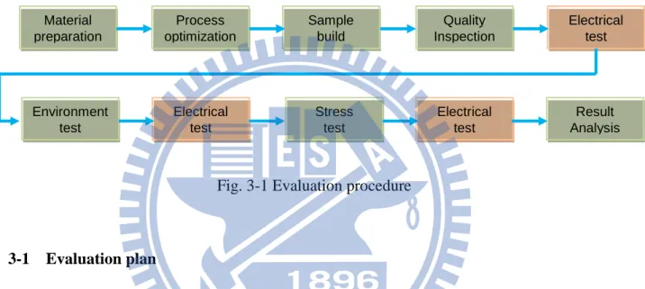
Fig. 3-1 Evaluation procedure
3-1 Evaluation plan
There are four types of materials included in flip chip package, solder material, substrate,
underfill and chips with bumps. In this study, we focus on the package performance on the
reliability for surface mount technology process, so the considered factors in this experiment
are solder materials and surface treatment of lead frame. For chips with copper pillar bumps
and underfill materials, we fix these factors in this evaluation.
The flip chip chip-scale package (CSP) is chosen for this experiment and the package
structure is shown as below Figure 3-2. For CSP, it means the package must have an area no
greater than 1.2 times of the chip size and it must be a direct surface mountable package. On
this package, the stress between interface layers is greater than that of conventional package,
thus CSP is a good candidate for this evaluation.
Material preparation Process optimization Sample build Quality Inspection Electrical test Environment test Electrical test Stress test Electrical test Result Analysis
-26- Lead Chip Bump Solder paste MUF
Fig. 3-2 Cross-section view of flip chip CSP package
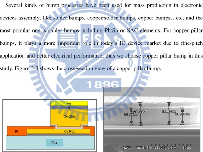
3-1-1 Fixed materials on the design of experiments (DoE) 1. Chip with copper pillar bump
Several kinds of bump processes have been used for mass production in electronic
devices assembly, like solder bumps, copper/solder bumps, copper bumps…etc, and the
most popular one is solder bumps including Pb/Sn or SAC elements. For copper pillar
bumps, it plays a more important role in today’s IC device market due to fine-pitch
application and better electrical performance, thus we choose copper pillar bump in this
study. Figure 3-3 shows the cross-section view of a copper pillar bump.
Fig. 3-3 Cross-section view of a copper pillar bump
The composition of a copper pillar bump is Cu/Ni/ Au, and the thickness of each layer
is Cu : 22um, Ni: 2-3um and Au: 5um. The purpose of gold layer is to prevent the
-27-
for electrical test, as shown in Figure 3-4. The daisy-chain pattern is a method of
propagating signals along a bus in which bumps/ pads are connected in series and the
signal passed from one bump to the next.
Fig. 3-4 Top view of chip with daisy-chain design
Copper pillar bump process contains two major parts, redistribution layer (RDL) and
bump. The process flow of RDL includes polymide coating, lithography, developing,
electroplating and photoresist stripping. The process flow of copper pillar bumping is as
shown in Figure 3-5, photoresist coating, exposure, developing, electroplating,
photoresist stripping, under bump metallurgy(UBM) removal and annealing.
-28-
2. Molding under fill (MUF)
Molding underfill is a kind of polymer material which includes several composite
components, like epoxy resins, phenolic hardeners, catalysts, and release agents. The
purpose is to encapsulate semiconductor devices to prevent the defects from moisture,
crack, package stress and interfacial delamination.
Package warpage is one of the major thermo-mechanical reliability concerns in
electronic packaging. The cause is come from CTE (Coefficient of Thermal Expansion)
mismatch on materials which comprise in a package. The occurrence of warpage during
the assembly process can lead to misalignment of parts and a variety of operational
failures. [15 ]
Kyocera low stress molding underfill is chosen for this experiment. With this material,
we can lower the process variation during the sample assembly, therefore, the test result
should be more reliable. The Table 3-1 shows the material property of a Kyocera molding
-29-
Table 3-1 The property of molding underfill
3-1-2 Key factor materials on the design of experiments (DoE) 1. Solder paste
Solder paste is the key material used in the process of surface mount technology.
It includes a sticky mixture of flux and tiny solder particles. Flux is added to act as a
temporary adhesive, holding the components until the solders melt in the soldering process,
leading to a stronger physical connection. The purpose of solder paste is to connect the
leads of IC packages to attachment points. The solder paste is chosen based on its intended
use purpose. In this experiment, we refer to the study of Ikuo Shohji in 2005, the SAC base
solder pastes have better workability and reliability, so three types of solder pastes are
-30-
a. SAC305 solder paste
Component: 96.5Sn/3Ag/0.5Cu, particle size: 15~5 um
b. SAC300 solder paste
Component: 96.5Sn/3.5Ag, particle size: 15~5 um
c. SAC405 solder paste
Component: 95.5Sn/4Ag/0.5Cu, particle size: 15~5 um
Fig. 3-6 Solder paste
Table 3-2 Comparison table of solder pastes
A (SAC305) B (SAC300) C (SAC405)
Melting point, o C 217~221 221~225 217~219 reflow temperature, o C 238~248 238~248 238~248 Coefficient of Thermal Expansion (20-100) 21.6 21.5 21.8 Electrical Resistivity , (μohm-cm) 13.0 12.3 12.7 Tensil Strength, MPa 41.1 40.6 43.7 Thermal Conductivity,
W/m.K
63.2 62.6 61.1 Elengation 41.0 41.2 40.6 Young’s Modulus, GPa 50 50 52 Poison’s Ratio 0.36 0.36 0.35
-31-
The added flux on above materials is the same and the change item is focused on the
component percentage of tin, silver and copper.
2. Surface treatment of lead frame
The surface treatment is to plate gold above the copper layer to prevent oxidation on
the surface, which can cause poor adhesion or cold joint on the solder-joint interface
between bump and substrate. In addition, the worst issue is the micro-crack defect
penetrating the package and resulting IC device function fail.
In this experiment, we use the lead frame material for CSP package. Two treatments
are considered in parallel, one is gold treatment and another one is pure copper treatment.
a. Pure Copper Leadframe (LF), as shown in Figure 3-7
b. Gold(Au) plated Leadframe (LF)
-32-
3-1-3 Design of experiments (DoE) matrix
A full factorial experiment is designed in this study. There are two factors that contain
two and three levels, respectively. Total 6 cells (2x3 matrix) are generated in this experiment.
The below table shows the detail of the full factorial DoE:
Cell
leadframe
Solder type
Remark
1
LF-PPF
Solder -A
SAC305
2
LF-PPF
Solder -B
SAC300
3
LF-PPF
Solder -C
SAC405
4
LF-Cu
Solder -A
SAC305
5
LF-Cu
Solder -B
SAC300
6
LF-Cu
Solder -C
SAC405
Table 3-3 The full factorial DoE
Two reliability tests are performed in this study, thermal cycling test (TCT) and pressure cooking test ( PCT). Therefore, total 300 units (50 ea x 6 cell) will be prepared in the test.
3-2 Examination items for process check
To verify whether the quality of samples can meet the requirement of the test, there are
several examination items employed in this study. These inspections are very important and
essential; the purpose is to assess the feasibility of the SMT process and material whether can
-33-
1. Die shear testing
Die shear testing is a method to determining the strength of adhesion on a
semiconductor chip to the attach lead frame. A shearing stress is performed and
subjected on the chip to examine the overall quality of adhesion interface. The pass
criteria is based on the definition of the MIL-Std-883 method 2019 as appendix 1, it
depends on the strength of the bonding area.
Fig. 3-8 The die shear testing method
2. X-ray inspection
X-ray inspection is a non-destructive analysis technique. The method is to use
X-radiation that is a form of electromagnetic radiation to penetrate the package and
inspect the image which is transformed by the scattered energy.
After molding process, the solder connections are underneath the chip and not visible
by optical microscope inspection. The use of X-ray inspection is to ensure that the
manufacturing process is able to accommodate the quality requirement.
-34-
a. Dry joints due to insufficient solder
b. Bridging/Shorts due to surplus solder
c. Voiding due to gas bubbles within the solder
d. Misplacement/Misalignment due to inaccurate placement of chip
3. Scanning Acoustic Microscopy (CSAM) inspection
Scanning Acoustic Microscopy (SAM) is a quick analysis technique without
destroying the package. SAM uses ultrasound waves to detect changes in acoustic
impedances in integrated circuits (IC) and other similar materials, pulses of different
frequencies are used to penetrate various materials to examine different interfaces and
determine the mechanical integrity of the assembly.
The following categories can be observed in this test:
a. Internal voids due to parameter or underfill issue
b. Interface delamination due to material CTE mismatch
c. Dry joints due to insufficient solder
d. Missing bump due to poor adhesion issue
4. Electrical test
The Ohmic testing is used to measure the resistance and analysis the electrical
performance. The resistance increases as the interconnection condition declines and can
be traced by the Ohmic measurement system. The resistance test can be performed as
two-wire measuring as well as with the high-accuracy 4-wire measuring. Precise and
stable measuring results up to the mOhm-range are detected. Figure 3-9 shows the
-35-
Fig. 3-9 The HP-34970A Ohmic testing equipment
5. Environment test
The environment test is to simulate the packaging, handling of electronic devices
which are sensitive for the introduction of moisture. When moisture traps inside packages
can damage them during soldering, as the moisture vaporizes and expands. The
expansion of trapped moisture can result in internal delamination of the package from the
die or lead-frame, and cause internal cracks.
We expect to simulate the strict use condition in this test, hence the Moisture
Sensitivity Level (MSL) requirement is Level 1 and the condition is as below:
Condition : 85℃ temperature, 85% RH and 168 hrs aging time.
6. Stress test
Temperature and humidity are major causes to make IC package failure, below
tests are applied in this study.
Temperature cycling test (TCT) - the thermal expansion mismatch among different
components of the package especially on the solder joint can be enhanced. Figure 3-10
shows the Hitachi ES63LMV Temperature cycling test oven.
Pressure cooking test (PCT) - the humidity impact and metal joint corrosion on the
-36-
model and calculate the acceleration factor, therefore, the time-to-failure distribution in
normal use condition can be estimated. Figure 3-11 shows the HIRAYAMA PC-242HS
pressure cooker.
The detail test conditions are as below:
a. Pressure cooker test (PCT), Condition : 121℃, 100% RH,
100/ 200/ 300/ 500/ 1000 hours
b. Temperature cycling test (TCT), Condition : -65℃, +150 ℃,
100/200/500/1000/1500/2000/3000/ 3500 cycles
Fig. 3-10 HITACHI Temperature cycling test oven
Fig. 3-11 HIRAYAMA Pressure cooker
3-3 Process optimization
-37-
solder joint interface between copper pillar bump and lead frame is also the key point. The
below lists the machine information and process flow for SMT
1. Machine type:
a. Chip / component place machine: Fuji NXP -1450 with integrated wafer handler
function, as shown in Figure 3-12
Fig. 3-12 Fuji NXP chip place machine
b. Auto optical inspection machine: OMRON-3F5VT
Cyber-FLEX ULTRA 8
c. IR reflow oven: BTU-PYRAMAX,
-10 Zone heating Oven
- Maximum temperature rating (all zones): 350°C
- Oven atmosphere: Air/N2
-38-
Fig. 3-13 BTU IR reflow oven
2. Operation procedure of surface mount assembly:
a. Cover stainless stencil on topside of lead frame
b. Print solder paste on the land of Lead frame/ substrate
c. Place bare die on lead frame land area
d. Auto optical inspection (AOI) for quality control
e. IR reflow process to fix the chip and Flux cleaning, Figure 3-15 shows the IR
profile
-39-
Fig. 3-15 IR-reflow profile
3. DoE for bonding join strength optimization
Solder paste is the key material to join the copper pillar and lead frame, if the solder
paste is insufficient, it may cause the poor bonding strength and affect the reliability. The
process optimization and affected factors are reported [16, 17]. To make sure the
bonding strength in the best condition, the process optimization to fit this experiment is
an essential work. We design four different opening of printing stencils and they are
100um / 125um/ 150um/ 180um opening. The purpose is to control the solder paste
printing size and thickness.
Test Parameter:
a. Printing speed : 20 mm/s
b. Printing pressure : 6.0 kg
c. Cycle time : 29.2 sec
-40-
Test method:
a. Die shear testing for bonding strength adjustment is performed
b. Appearance check after solder paste printing
Fig. 3-16 Solder plating on copper lead frame
Test result
From die shearing test result, the 150um and 180um opening tools can meet the
requirement. Comparing to 150um and 180um opening tools, the solder height of 180um
is higher than that of 150um opening, it has risk to bleed out the solder paste and
-41-
Fig. 3-17 Appearance check result of solder paste printing by different stencil opening
Fig. 3-18 Abnormal photo for insufficient solder
After the test and data analysis, the printing stencil with 150um opening got better
performance and met the quality requirement, the thickness of solder paste also can
-42-
3-4 Test sample manufacturing
After process optimization, the best condition for sample manufacturing is determined.
We implement it on the Flip-chip CSP assembly process and confirm the samples quality to
meet our requirement.
3-4-1 The assembly process flow
There are several processes in package assembly, here we list the major process flow:
1. L/P : the process is to grind the wafer to the designate thickness
2. D/S : to saw the wafer to the unit by high speed diamond blade
3. Chip attach : to bond the chip on the lead frame or substrate
4. IR reflow : an oven with several heating zones for soldering process
5. M/D : molding, to encapsulate the chip with molding underfill material
6. S/P : solder plating, to plate the tin on the outer lead, this process is for lead package
only
7. P/S : package sawing, to cut the leadframe/ substrate into units
-43-
Fig. 3-19 FC CSP process flow
3-4-2 Quality inspection result
Quality inspection is about inspection, measuring, or testing of product characteristics. To
make sure all samples can meet the quality requirement and can release to next evaluation
without abnormal phenomenon, we perform tests in production.
1. Appearance inspection
The optical microscope is used to check the outlook quality. All units are inspected
and the test result can meet the specification on solder paste print, bonding position
-44-
Fig. 3-20 The appearance inspection
-45-
2. Die shear testing
The die shear testing for six cells has been done to confirm the solder joint strength.
Fifteen units per cell are examined and the result could pass the specification. The defect
mode after shear testing is solder ball-neck broken, and this failure phenomenon meets
the standard. The test readings are listed on Table 3-4.
The cell 4, cell5 and cell 6 with bare copper LF got better test result, there is no
significant test difference from cell 1 to 3 and the PPF treatment lead frame is used in
these cells.
unit: Kg
Table 3-4 The shearing test result
Cell 1 2 3 4 5 6 1 0.959 1.083 0.967 3.257 3.288 3.213 2 1.185 0.995 0.883 3.033 3.088 3.262 3 0.887 0.954 0.882 3.183 2.672 3.332 4 1.168 1.068 1.083 3.446 3.249 3.397 5 0.852 0.877 0.928 2.541 2.751 3.078 6 0.895 0.898 0.868 3.332 2.825 3.208 7 1.126 1.078 0.892 3.193 3.014 3.574 8 0.994 0.874 1.048 3.224 3.279 3.334 9 0.972 1.056 0.961 3.206 2.905 2.687 10 1.254 0.931 0.898 2.948 3.016 3.275 11 1.065 0.956 1.218 3.152 2.962 3.078 12 0.986 1.185 0.922 2.913 3.303 2.875 13 1.169 0.848 0.972 3.101 3.011 3.371 14 1.193 1.021 1.025 2.763 2.694 2.986 15 1.194 0.908 1.017 3.228 2.948 3.258 max 1.254 1.185 1.218 3.446 3.303 3.574 min 0.852 0.848 0.868 2.541 2.672 2.687 mean 1.060 0.982 0.971 3.101 3.000 3.195 sigma 0.132 0.097 0.095 0.231 0.212 0.224 Spec 0.080 0.080 0.080 0.080 0.080 0.080 Ppk 2.469 3.092 3.122 4.357 4.589 4.643
-46-
Fig. 3-22 Die shearing test analysis
Fig. 3-23 The breaking mode after die shearing test
3. X-ray inspection
The X-ray inspection has been done for six cells to confirm the solder joint
-47-
under bump connection interface should be scraped.
Fig. 3-25shows the X-ray inspection result for normal unit.
Fig. 3-24 The X-ray inspection result for a defect unit
Fig. 3-25 The X-ray inspection result for normal units
4. Scanning Acoustic Microscopy (CSAM) inspection
CSAM inspection is confirmed for six cells to exam the delamination in different
interfaces within packages. Figure 3-26 shows the result of normal units and defect units.
All units are inspected and the result could pass the specification. No delamination
-48-
Fig. 3-26 CSAM inspection result of normal units and defect units
5. Cross sectioning inspection
After package separation process, we performed cross-section to confirm the
package structure, chip tilt. The unit is grinded from side of package to bonding area and
inspected by optical microscope. No abnormal phenomenon was found in the sample.
-49-
6. Electrical test
The judgment of reliability test is based on the electrical test results, therefore, all
samples are confirmed by electrical test. We use high-accuracy 4-wire measuring system
in the test. Table 3-5 shows all initial test readings of resistance. From the test results, the
cell 1 to 3 show higher resistance than those of cell 4 to 6 and that is due to the solder
plating thickness deviation of package outer-lead. The data is for reference only, because
we judge the device by open or short condition.
Unit: mOhm
Table 3-5 Initial resistance measurement data
unit Cell-1 Cell-2 Cell-3 Cell-4 Cell-5 Cell-6
1 56 46 54 46 41 48 2 49 48 48 46 48 50 3 51 48 49 48 46 47 4 58 48 50 48 43 47 5 48 46 46 48 44 48 6 53 52 56 48 44 52 7 50 56 59 48 48 48 8 46 54 51 48 45 49 9 46 60 56 52 44 50 10 51 53 54 48 47 51 11 57 60 57 48 49 44 12 55 57 58 48 45 46 13 55 45 59 48 49 48 14 49 49 60 48 45 49 15 56 59 52 50 45 48 16 51 52 52 53 44 44 17 54 53 54 48 44 50 18 52 53 54 48 44 48 19 50 56 48 46 47 51 20 54 51 59 39 46 49 21 52 52 59 44 47 48 22 55 52 52 46 50 50 23 51 58 59 46 46 45 24 53 51 52 48 46 42 25 48 49 53 46 46 49
-50-
Chap 4. Evaluation Result Analysis
In this chapter, we confirm the feasibility assessment of surface mount assembly for flip
chip CSP package application and analyze the reliability test result including Weibull
distribution, fail point in stress test and the defect mode analysis.
4-1 Pressure cooker test (PCT) failure distribution
Through the resistance measurement method on the package with daisy-chain design, we
can know the electrical performance precisely. All units in six DoE Cells are measured after
every test point. The test points are 100, 200, 300, 500, 1000 hours. The below table is the
failure distribution. Check points PCT 0hr PCT 100hrs PCT 200hrs PCT 300hrs PCT 500hrs PCT 1000hrs Cell 1 0 0 0 0 1 3 Cell 2 0 0 0 1 2 4 Cell 3 0 0 0 1 2 5 Cell 4 0 0 0 0 0 2 Cell 5 0 0 0 0 0 3 Cell 6 0 0 0 0 0 2
Table 4-1 PCT test result
We observed the first failure point is at PCT 300 hours for cell 2 and cell 3. Based on the
JEDEC standard definition, the pass criteria is 168 hours, so all these units can meet this
requirement and have no concern on the reliability performance. For the test results of other
cells, we see cell 1, the first failure point is at 500hrs and cell 4, cell 5 and cell 6, the failure
-51-
4-2 Temperature cycling test (TCT) failure distribution
Following the resistance measurement method as PCT, all units in six DoE Cells are
measured after every test point. The test points are 100, 200, 500, 1000, 1500, 2000, 3000 and
3500cycles. The below table is the failure distribution.
Table 4-2 TCT test result
We observed the first failure point is at TCT 200 cycles for cell 1 and cell 2, for cell 3, the
failure point is at TCT 500 cycles, for cell 4, cell 5 and cell 6, the first failure point is at TCT
3000 cycles. Based on the definition of JEDEC standard, the pass criteria is 1000cycles, so
test units from cell 4, cell 5 and cell 6 can meet this requirement.
Table 4-3 shows the electrical test result, we measured the resistance after every test points
and then generated the chart using average data. We observed the electrical performance was
stable for cell 4, cell 5 and cell 6. The cell 1, cell2 and cell 3 shows worse resistance after
TCT 500C test, and the same lead frame material are used for these three cells.
Cycles MSL 1 TCT 100c TCT 200c TCT 500c TCT 1000c TCT 1500c TCT 2000c TCT 3000c TCT 3500c Cell 1 0 0 2 3 6 8 12 17 -Cell 2 0 0 1 4 8 10 14 19 -Cell 3 0 0 0 2 3 5 9 14 -Cell 4 0 0 0 0 0 0 0 2 3 Cell 5 0 0 0 0 0 0 0 1 3 Cell 6 0 0 0 0 0 0 0 2 3
-52-
Table 4-3 Resistance measurement after TCT test
4-3 Weibull distribution
From the reliability test result in the PCT and TCT test, the Weibull distribution can be
drew to model the lifetime data. Through the equation (2-4) we discussed in chapter 2.-2-2,
we can find the shape parameter (β) and characteristic life time (η).
𝑓𝑓T(t) = βη�t−γη � β−1
e−�t−γη � β
, t ≥ γ (2-4)
A commercial software - Mimitab is used for data calculation and result analysis in this study. Mimitab is distributed by Minitab Inc, and is a powerful statistic and process
management software which is used in statistics-based process improvement methods, like Six-sigma, DoE, reliability and other statistics-based process improvements.
-53-
4-3-1 Weibull distribution for PCT
The experimental result and time interval are fitted into the Minitab software and use the
Reliability/ Survival function to analysis these data, the distribution is drew, and then the
shape parameter (β) and characteristic life time (η), hazard rate (h) can be estimated.
-54-
Fig. 4-2 Weibull distribution for PCT Cell-2
-55-
Fig. 4-4 Weibull distribution for PCT Cell-4
-56-
Fig. 4-6 Weibull distribution for PCT Cell-6
The shape parameter (β) for all 6 cells are larger than one, it means the distribution that
can meet the Weibull normal distribution. The shape parameter and the scale parameter for 6
cells are summarized as following table.
Cell 1 Cell 2 Cell 3 Cell 4 Cell 5 Cell 6
Shape parameter (β) 2.69 2.26 3.69 2.9 3.05 2.78
Scale parameter (η) 2720 1049 1131 3648 2797 3958
-57-
4-3-2 Weibull distribution for TCT
Following the same method, we input the failure result and time interval into the Minitab
software and use the Reliability/ Survival function to analysis these data, the shape parameter
(β) and characteristic life time (η), hazard rate (h) can be estimated.
-58-
Fig. 4-8 Weibull distribution for TCT Cell-2