國 立 交 通 大 學
電機學院與資訊學院 電子與光電學程
碩 士 論 文
降低不匹配效應之二階 Σ
-Δ
類比至數位轉換器
A Compensation Technique for Reducing Mismatch
Errors of CMOS Second-order MASH Σ-∆ ADC
研 究 生:歐欣華
指導教授:吳重雨 博士
降低不匹配效應之二階 Σ
-Δ 類比至數位轉換器
A Compensation Technique for Reducing Mismatch Errors
of CMOS Second-order MASH Σ-∆ ADC
研 究 生:歐欣華
Student: Hsin-Hua Ou
指導教授:吳重雨 博士
Advisor: Dr. Chung-Yu Wu
國 立 交 通 大 學
電機學院與資訊學院 電子與光電學程
碩 士 論 文
A ThesisSubmitted to Degree Program of Electrical Engineering and Computer Science College of Electrical Engineering and Computer Science
National Chiao Tung University in partial Fulfillment of the Requirements
for the Degree of Master of Science
in
Electronics and Electro-Optical Engineering January 2006
Hsinchu, Taiwan, Republic of China
降低不匹配效應之二階 Σ
-Δ 類比至數位轉換器
研究生:歐欣華
指導教授:吳重雨 博士
國立交通大學電機學院與資訊學院 電子與光電學程﹙研究所﹚碩士班
摘
要
本論文提出一個有效架構來降低二階MASH (multistage noise shaping) 類比數位轉 換器之不匹配效應。因製程偏差所造成之電容不匹配效應會造成類比數位轉換器之訊噪 比下降,此新架構利用資料流的交互轉換,有效補償電容不匹配效應所造成之影響。透 過國家晶片系統設計中心委託台灣積體電路製造股份有限公司以 0.35 微米互補式金氧 半導體的製程製造。整個類比數位轉換器已經被完整地設計、製造與量測完成。 為了比較新架構比起傳統架構更能有效抑制電容不匹配效應所造成之影響,同時將 兩種架構放進晶片中,並刻意製造 20% 之電容不匹配。量測結果顯示,新架構之訊噪 比幾乎不受電容不匹配所影響。傳統架構的佈局面積是600x1500 µm2;新架構的佈局面 積是700x1500 µm2。在3v的操作電壓,22.05kHz 的輸入訊號,取樣頻率為 5.6448MHz 下,量測到之訊噪比為68.8dB;1kHz 的輸入訊號,取樣頻率為 256kHz下,量測到之訊 噪比為90.6dB
A Compensation Technique for Reducing Mismatch Errors
of CMOS Second-order MASH Σ-∆ ADC
Student: Hsin-Hua Ou
Advisor: Dr. Chung-Yu Wu
Degree Program of Electrical Engineering Computer Science
National Chiao-Tung University
Abstract
A compensation technique for reducing mismatch errors of CMOS second-order MASH (multistage noise shaping) delta-sigma analog to digital converter (ADC) is proposed in this thesis. The signal-to-noise ratio (SNR) of ADC will reduce due to the mismatch of capacitors by process variation. An innovative compensation method which re-locate data path by switched capacitor is realized in a 0.35-µm CMOS technology supported by Taiwan Semiconductor Manufacturing Company via Chip Implementation Center. The proposed ADC is completely designed, fabricated and tested.
Both conventional and new proposed architectures are on the chip, and 20% capacitor mismatch is placed on purpose. Measured results exhibit that the new proposed MASH has better immunity to capacitor mismatch errors effect than conventional MASH. The chip area of conventional MASH is 600x1500µm2; the new proposed MASH is 700x1500µm2. Measured SNR is 68.8dB with 22.05 kHz input signal and 5.6448MHz sampling rate; 90.6dB with 1 kHz input signal and 256 kHz sampling rate in 3v supply voltage.
誌
謝
能夠順利完成碩士論文,首先要感謝我的指導教授吳重雨老師;在研究所的這三年 半裡,老師提供我一個良好的學習環境,並且在學習與研究上適時的給予我指導與啟發 ,嚴謹的研究精神以及對人謙虛和善的態度,使我受益良多。其次要感謝論文口試的評 審委員,陳巍仁教授、柏振球教授與廖以義博士對我的論文提出了許多建議,使我的論 文內容更加完整。 再來要感謝實驗室的學長們,施育全學長、林俐如學姊、陳勝豪學長、蘇芳德學長 、王文傑學長、虞繼堯學長、蘇烜毅學長、林韋霆學長們給予我的幫助與指點和研究上 的經驗傳承。同時也要感謝公司的主管們讓我有再進修的機會,常常必須中斷工作請假 到學校,以及感謝同事炳輝在佈局上的協助與指導。也感謝吳諭、煒明、家熒、文芩、 衛宗、志遠、汝玉、豪傑、怡凱、允斌,在學校瑣事的幫忙,並陪伴我度過這段研究生 活,也增添了許多歡笑與回憶。 最後,要感謝我的父母以及女友令君,當我面臨壓力時鼓勵我,給我繼續前進的動 力,當我研究繁忙時體諒我,讓我可以全心衝刺。 謹以此篇論文獻給所有關心我的人。CONTENTS
Chinese Abstract
i
English Abstract
ii
Acknowledgement iii
Contents iv
Table Captions
vi
Figure Captions
vii
Symbol Description
x
CHAPTER 1
Introduction
1
1.1 Background and Review 1
1.2 Motivation 7
1.3 Main results 7
1.4 Thesis organization 8
CHAPTER 2 Architecture design and operational principle
9
2.1 Conventional MASH 92.2 Mismatch effect 11
CHAPTER 3
Circuit implementation 18
3.1 Analog circuit realization 183.1.1 Gain boosting CMFB OPAMP 18 3.1.2 Integrator 24 3.1.3 Quantizer 28
3.2 Digital circuit realization 30
3.2.1 Switched-capacitor implementation and C-ratio mismatch control 30 3.2.2 Logic circuit and digital cancellation 34 3.2.3 System design 37
3.3 Simulation results 41
3.3.1 Matlab (Simulink) simulation results 41 3.3.2 Hspice simulation results 45
CHAPTER 4
Experimental results 47
4.1 Layout descriptions 48 4.2 Testing environment 50 4.3 Experimental results and discussions 52
CHAPTER 5
Conclusions and future work 60
Table Captions
Table I Gain factors in the modulator. 38 Table II Capacitor values in the modulator. 40 Table III Summary of simulation results 46
Table IV Summary of specification 46
Table V The simulated and measured characteristics 58 Table VI Compare the measurement results with surveyed paper 58
Figure Captions
Fig. 1 Feed-forward modulator 1 Fig. 2 MASH (Multi-stage noise shaping) 3
Fig. 3 Block diagram of the pole error compensation technique 4 Fig. 4 The implementation of the pole error compensated integrator. 4
Fig. 5 Uni-MASH architecture. 5 Fig. 6 Block diagram of the digitally corrected MASH modulator. 6
Fig. 7 Cascaded delta-sigma modulator with compensation. 6 Fig. 8 Block diagram of second-order of conventional MASH 9 Fig. 9 Some different noise-shaping transfer functions.[8] 11 Fig. 10 Block diagram of second-order of conventional MASH with mismatch effect 13
Fig. 11 Block diagram of new proposed MASH 14 Fig. 12 Time- and capacitor- multiplexing switched-capacitor integrator [3] 15
Fig. 13 Quantization error with “ramp” signal 16 Fig. 14 Fully differential gain boosting CMFB OPAMP 19
Fig. 15 NMOS-input fully differential gain boosting amplifier with continuous time CMFB 20 Fig. 16 PMOS-input fully differential gain boosting amplifier with continuous time CMFB 21
Fig. 17 Gain and phase margin with AC response of the boosting amplifier 22
Fig. 18 Increasing the output impedance by feedback.[17] 23 Fig. 19 Gain and phase margin with AC response of the main OPAMP 23
Fig. 20 Basic first-order Sigma-delta modulator 24 Fig. 21 Fully differential first-order integrator 25
Fig. 22 (a) switched-capacitor unit (b) four-phase non-overlapping clock 25 Fig. 23 MOS switch (a) symbol; (b) single-MOSFET realization; (c) equivalent circuit 26
Fig. 24 First-order A/D modulator: [8] (block diagram and switched-capacitor
implementation) 27 Fig. 25 Response of a fast comparator (a) without hysteresis (b) with hysteresis 28
Fig. 26 The schematic of latch comparator with hysteresis 29 Fig. 27 The .DC simulation result of latch comparator with hysteresis 30
Fig. 28 The .Tran simulation result of latch comparator with hysteresis 30 Fig. 28 Non-overlapping clocks (a) clock signal, φ1 and φ2. (b) A possible circuit 31
Fig. 29 The schematic of four-phase non-overlapping clock generation 32 Fig. 30 The simulation result of four-phase non-overlapping clock generation 32
Fig. 31 The schematic of control circuit 33 Fig. 32 The simulation result of control circuit 34 Fig. 33 divide one sampling period into two phases 35 Fig. 34 Clock generation circuit for new proposed MASH 36
Fig. 35 digital delay circuit (a) z-1 (b) z-1/2 36 Fig. 36 2nd-order 1-1 cascaded Sigma-delta modulator with system coefficient. 37
Fig. 37 Gain factors in the modulator. 39 Fig. 38 SC-implementation of conventional 1-1 modulator. 39
Fig. 39 SC-implementation of new proposed 1-1 modulator. 40 Fig. 40 The Simulink model of conventional 1-1 modulator structure 42
Fig. 41 The Simulink model of new proposed 1-1 modulator structure 43 Fig. 42 The Simulink simulation results of conventional MASH 43 Fig. 43 The Simulink simulation results of new proposed MASH 44 Fig. 44 The Simulink simulation results between different mismatch 44
Fig. 46 A double-poly capacitor 49 Fig. 47 A parasitic-insensitive integrator with parasitic capacitance 49
Fig. 48 The environment setup of measurement 50 Fig. 49 The PCB layout of test board (a) top plate (b) bottom plate 51
Fig. 50 The photograph of the PC test board 52 Fig. 51 The logic analyzer waveform of conventional MASH 52
Fig. 52 The logic analyzer waveform of new proposed MASH 53 Fig. 53 The measurement spectrum of conventional MASH without mismatch (OSR=128)
54 Fig. 54 The measurement spectrum of conventional MASH with 20% mismatch (OSR=128) 54 Fig. 55 The measurement spectrum of new proposed MASH without mismatch (OSR=128) 55 Fig. 56 The measurement spectrum of new proposed MASH with 20% mismatch(OSR=128) 55 Fig. 57 The measurement spectrum of conventional MASH without mismatch (OSR=128) 56 Fig. 58 The measurement spectrum of conventional MASH with 20% mismatch (OSR=128) 56 Fig. 59 The measurement spectrum of new proposed MASH without mismatch (OSR=128) 57 Fig. 60 The measurement spectrum of new proposed MASH with 20% mismatch(OSR=128) 57
Symbol Description
Σ : sigma ∆ : delta
MASH : multistage noise shaping ADC : analog-to-digital converter SNR : signal-to-noise ratio NTF : noise transfer function STF : signal transfer function OSR : oversampling ratio CMFB : common mode feedback DAC : digital-to-analog converter SC : switched capacitor
PCM : pulse code modulation ENOB : effective number of bits
CHAPTER 1
Introduction
1.1 Background and Review
Sigma-delta data converters are widely used, particularly in applications where high precision is required and the signal band is relatively small, such as in the processing of audio and sensor signals. The analog-to-digital (A/D) converters, based on the use of oversampling and sigma-delta modulation followed by the decimation process, are currently the most popular converters for audio applications. In addition, the requirements for the external anti-aliasing filters are highly relaxed by the internal decimation process following the modulation. For example, usually only a first order anti-aliasing filter is required for A/D converters, which can often be realized on chip or at worst case very inexpensively off chip. A fundamental choice in the design of the modulator is whether to use a single loop structure or cascade (MASH-multistage noise shaping) architecture. Both the solutions have advantage and drawback, which have been list as below:
The block diagrams of single loop Sigma-delta modulator have two kinds of method, single loop and MASH, which are shown in Fig. 1 [1] and Fig. 2.
There are main advantages of the single loop architecture [1]:
It is intrinsically insensitive to components non-idealities. Large capacitor mismatches are well-tolerated;
Low-gain operational amplifiers are easily tolerated, so the large bandwidth requested is easier to be achieved;
Slew rate effects are important mainly in the first resonator and linear but incomplete settling does not affect the performance (at first order), leading only to an op-amp gain error and consequently rejected;
A single loop structure gives better flexibility in the choice of the noise transfer function (NTF) and signal transfer function (STF) allowing zeros and poles spreading;
Decimation and filter processes are slightly easier. But there are also some problems with this kind of architecture:
It suffers of instability. In order to obtain a conditional stability a single loop must have a less “aggressive” NTF in comparison with a cascade modulator. As a consequence, for the same order, the quantization noise in a single loop will be higher than in a cascade;
Single loop needs stabilization circuitry; Single loop is inherently tonal.
As mentioned above, a cascaded sigma-delta modulation has been developed in the design of high performance analog-to-digital converter for preventing the stability problem. The block diagram is shown in Fig. 2. The quantization error of a low order converter is processed as an input, and ideally the resulting conversion is equivalent to that of a single stage converter of order equal to the sum of the orders of all individual stages.
Fig. 2 MASH (Multi-stage noise shaping)
Let’s give a look now to the advantages of the cascade (MASH) architecture:
It is inherently stable, because it is composed by stable (1st and 2nd order)
sub-structures;
The NTF can be more “aggressive”, which means a higher dynamic range (DR) (due only to quantization noise) for the same oversampling ratio (OSR) and order; A cascade structure is less tonal.
The loop coefficients are easy to be implemented. The disadvantages of this solution may be resumed as follows:
The cascade suffers greatly from components mismatches between the two loops, and thus the layout of the modulator becomes a big issue;
The op-amp gain must be as higher as possible in order to avoid noise leakage; Any settling problem in any section of the two loops leads to gain reduction and
transfer function mismatches, which degrade modulator performance.
The mismatch issue for MASH has already become a topic which is discussed in some papers. Some are used by analog circuits, and some are used by digital method. The surveyed papers are list below with brief introduction.
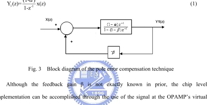
A compensation technique for integrator’s pole error in cascaded sigma-delta modulators [2].
First, a pole-error compensation is shown as Fig. 3. Giving a positive feedback gain β to the uncompensated integrator eliminates completely the integrator pole error, thus making the overall integrator insensitive to the OPAMP gain. The transfer function can be obtained as equation (1). 1 -1 (1- ) Y (z)= x(z) 1-z α (1)
Fig. 3 Block diagram of the pole error compensation technique
Although the feedback gain β is not exactly known in prior, the chip level implementation can be accomplished through the use of the signal at the OPAMP’s virtual ground. The implementation of the compensated integrator with positive feedback through a buffer circuit is shown in Fig. 4. This method has two drawbacks, one is an additional OPAMP is needed for compensation; another is only pole error mismatch reducing, gain error is still alive to suffer the SNR.
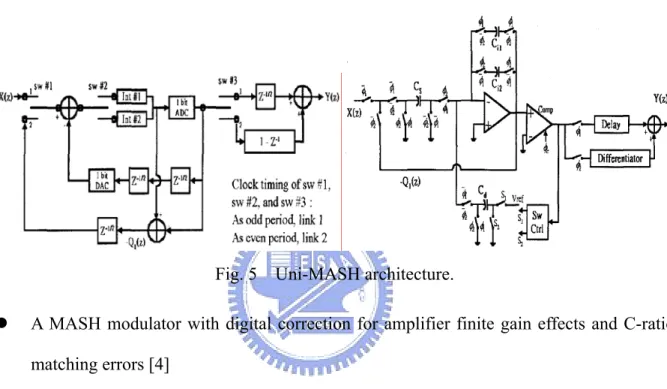
Gain mismatch effect of cascaded sigma delta modulator reduced by serial technique [3] The transfer function of two-stage MASH architecture realized by uni-MASH architecture in Fig. 5 is as equation (2):
Y=K1z-2 X +(K1-K1’)(1-z-1)z-1e1+K1’(1-z-1)2e2 (2)
The new proposed MASH first error coefficient is (K1-K2)*(e1-e2) which will be derived
later. Just note that (K1-K2)*(e1-e2) will smaller than (K1-K1’).
Fig. 5 Uni-MASH architecture.
A MASH modulator with digital correction for amplifier finite gain effects and C-ratio matching errors [4]
Another solution to reduce mismatch effect is by employing an additional digital correction block which compensates for the finite amplifier gain effects and capacitor ratio mismatches between subsequent stages. This is a 3rd order modulator as shown in Fig. 6. A0 is
the open-loop gain of a finite amplifier, and εm is the corresponding capacitor-ratio mismatch
error. Both of these two coefficients which are estimated must be added into the digital correction term. Not a fixed value to be estimated for every modulator, because the εm is
Fig. 6 Block diagram of the digitally corrected MASH modulator.
Adaptive compensation of analog circuit imperfections for cascaded delta-sigma ADCs [5].
In this paper, the approach to on-line adaptive correction, by adding a test signal as reference before the quantizer in first stage, minimum hardware complexity and robust adaptation can be achieved. As shown in Fig. 7, a compensation digital filter Lc plus an on-line adaptive algorithm is introduced to compensate. A random binary test signal, which acts as a reference for adaptation, is added at the first-stage quantizer input. The coefficients of the compensation filter are adjusted to minimize the power of the test signal in the modulator output through the least-mean-squares algorithm implemented with a correlator.
1.2 Motivation
As mentioned in chapter 1.1, we knew that instability is a serious problem for single loop sigma-delta modulation. The limitation of the high order sigma-delta modulation stems from the fact that high order integration can not be realized due to the oscillation of the feedback loop. In this case, the modulator would settle into large-amplitude low-frequency limit cycle and result in instability. To improve the stability of higher-ordered sigma-delta modulation, MASH is a promising architecture to permit high-order noise shaping factor without instability problem because it composes of several highly stable (first-order) sigma-delta modulation in cascade. The input of the next stage sigma-delta modulation is the quantization noise of the previous stage sigma-delta modulation. The quantization noises of the intermediate stage sigma-delta modulation are then all digitally cancelled. Thus only the quantization noise from the last stage sigma-delta modulation is left and MASH becomes always stable. However, there are still some defects in MASH architecture. For example, the quantization noise cancellation is sensitive to the gain matching accuracy between each stage of MASH. Based on MASH architecture, an architecture which is applied double sampling clock and time-division concept is proposed [3], and relocate data path of two first-order modulators to each other.
Develop a second order sigma-delta modulator architecture to reduce component mismatch errors effect of MASH.
1.3 Main
results
In order to specify the new proposed MASH structure which has better immunity to gain mismatch errors, both conventional MASH and new proposed MASH are placed on this chip. And place 20% mismatch capacitors circuit in the feedback loop DAC in purpose. This mismatch effect can be controlled by an external signal. This design is a second order Sigma-delta modulator which is considered as multistage noise shaping (MASH) and
designed in switched capacitor technique to achieve 1-bit quantizing at 5.6448MHz. The modulator was implemented in a TSMC 0.35µm four metal layers mixed-mode CMOS process from 3v power supply and the digital cancellation part and SNR calculation are simulated under Matlab. The A/D converters allow the transition between analogue and digital domains, while sampling the continuous analogue signal and quantizing it, the quantification is an essential stage of the conversion, it introduce to the effective signal a noise supposed white.
The total power consumption of conventional and new proposed MASH is less than 10mW when AVDD, DVDD and IOVDD are 3-volts:
1. The measured maximum SNR is 73.0dB in conventional MASH without capacitor-ratio mismatch.
2. The measured maximum SNR is 56.5dB in conventional MASH with 20% capacitor-ratio mismatch.
3. The measured maximum SNR is 68.8dB in new proposed MASH without capacitor-ratio mismatch.
4. The measured maximum SNR is 68.3dB in new proposed MASH with 20% capacitor-ratio mismatch.
1.4 Thesis
organization
In chapter 2, the difference of operational principle between conventional MASH and new proposed MASH are discussed. List all the formulas then show the immunity to gain mismatch errors based on mathematics theory. In chapter 3, the circuit design and software simulation are presented. In chapter 4, the layout descriptions, measurement results are presented. Finally, the conclusions and future works are given in chapter 5.
CHAPTER 2
Architecture design and operational principle
A key concern for the Sigma-delta modulator architecture design is to allocate maximum noise budget to analog noise (thermal and noise), since analog noise determines power dissipation and analog circuit size. A single-loop Sigma-delta modulator with more than two integrators will suffer from unstable oscillations for large level inputs which rapidly increases the quantization noise. So only use 1-1 MASH to ignore unstable issue [6]. The phenomenon is usually referred to as overload and is literally caused by overloading the 1-bit quantizer. So a variable reference voltage is used to prevent overloading between input signal and feedback quantity.
2.1 Conventional
MASH
MASH architectures require coupling the quantization noise of one stage to another, and this usually requires subtracting the quantizer output from its input. An example is the two-stage MASH shown in Fig. 8.
Quantization in amplitude and sampling in time are the two main functions of all digital modulators. Once sampled, the signal samples must also be quantized in amplitude to a finite set of output values.
The quantizer, embedded in any ADC is a non-linear system, is difficult to analyze. To further simplify the analysis of the noise from the quantizer, the following assumptions about the noise process and its statistics are conventionally made [7]:
1. The error sequence e[n] is a sample sequence of a stationary random process,
2. The random variables of the error process are uncorrelated; i.e. the error is a white-noise process,
3. The probability distribution of the error process is uniform over the range of quantization error.
Oversampling occurs when the signals of interest are band-limited to f0 yet the sample
rate is at fs, where fs>2f0 (2f0 being the Nyquist rate or, equivalently, the minimum sampling
rate for signals band-limited to f0) [8]. The order of the sigma-delta converter is defined as the
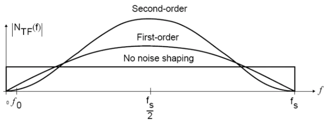
order of the loop transfer function. Signal-to-noise ratio (SNR) with different noise shaping is list:
Oversampling: SNRmax=6.02N+1.76+10log(OSR)
First-order noise shaping: SNRmax=6.02N+1.76-5.17+30log(OSR)
Second-order noise shaping: SNRmax=6.02N+1.76-12.9+50log(OSR)
0
2
sf
OSR
f
=
(3)Which N is the bit number of quantizer, OSR is oversampling ratio, fs is sampling
frequency, f0 is signal bandwidth.
Fig. 9. Note that over the band of interest (i.e., from 0 to f0), the noise power decreases as the
noise-shaping order increases. However, the out-of-band noise increases for the higher-order modulators [8]. The out-of-band noise will be filtered out after decimator.
Fig. 9 Some different noise-shaping transfer functions.[8]
Fig. 8 shows a second-order conventional MASH architecture. The outputs, Y1 and Y2, are fed into a digital cancellation network prior to the decimation filter. This cancellation network, based on a prediction of the analog inter-stage gain K (this will be described in next chapter), aims to cancel the quantization error from all but the last stage. The transfer functions from the input and the quantization-noise sources to the output are derived in the equations below.
Y1=z-1 X + (1-z-1)e1 (4)
Y2=- z-1e1 + (1-z-1)e2 (5)
Y= z-1*Y1 + (1-z-1)Y2=z-2 X +(1-z-1)z-1e1-(1-z-1)z-1e1+(1-z-1)2e2=z-2 X +(1-z-1)2e2 (6)
Here, signal transfer function (STF) isz-2 X; noise transfer function (NTF) is (1-z-1)2e2.
2.2 Mismatch
effect
In VLSI implementation, MASH architecture must tolerate finite gain in operational amplifier and capacitor ratio mismatch in the analog circuits [9]. The performance of Sigma-delta modulator is limited by several errors and noise source. In addition to the
system-level errors such as an inaccurate matching and a slow integrator settling, analog noise sources reduce the achievable SNR with the fundamental performance limiting noise source in switched-capacitor implementations being the thermal (kt/C) noise generated by capacitors [10]. Capacitor mismatch causes the gain error in a straightforward manner, since the gain of the integrator G is determined by the ratio of the sampling capacitor to the integration capacitor. Gain error is caused predominantly by the capacitor mismatches, finite DC gain, and incomplete linear settling due to the finite bandwidth of the op-amp. The pole error is inversely proportional to the DC gain of the op-amp. Thus, increasing the DC gain of the op-amp decreases the pole error. In general, the integrator transfer function can be written as [2][11].
( )
( )
-1 int -1(1- )z
H
z =G
1- 1-
z
α
β
(7)Where G is the gain of integrator, α is the gain error and β is the pole error. The nonzero pole error β causes a leakage of unshaped quantization noise to the output of the converter. Finite gain of an operational amplifier will cause a gain error and a pole error in a switched capacitor (SC) integrator. Both errors are inversely proportional to the gain. In order to focus on the mismatch effect, high DC gain of the op-amp is designed on chip to reduce the pole error effect.
Let the gain of each first-ordered Sigma-delta modulator be defined as the ratio between its digital output and analog input. As shown in Fig. 10, Y1 and Y2 are the ideal output at the
ideal first-ordered Sigma-delta modulator with gain is 1. K1Y1 and K2Y2 are the digital
Fig. 10 Block diagram of second-order of conventional MASH with mismatch effect Then the transfer function of the second-order conventional MASH becomes:
Y1=z-1 X +(1-z-1)e1 (8)
Y2=-z-1e1 +(1-z-1)e2 (9)
Y=K1z-1Y1 +K2(1-z-1)Y2=K1z-2X +K1(1-z-1)z-1e1-K2(1-z-1)z-1e1+K2(1-z-1)2e2 (10)
Apparently, the first stage quantization error is not exactly cancelled in reality such that performance degrades.
2.3 New proposed MASH
Recognizing the similarities in the different stage of MASH, I propose the new architecture illustrated in Fig. 11. An innovative method which re-locate data path by switched capacitor based on uni-MASH reduced the mismatch effect [3]. The operation principle is explained below. Fig. 11 shows the new proposed MASH by timing switch. Each sampling period is divided into timing phase 1 and timing phase 2. Timing phase 1 is correlated with first order stage of conventional MASH; timing phase 2 is correlated with second order stage of conventional MASH. At the beginning of first timing stage, switch 1
and switch 2 let the input to both modulators at the same time. Two relative switch 5 and switch 6 will be selected to store the integration value into different capacitors. Finally, switch 3 and switch 4 decide if the differentiator is necessary. Since the time division concept is employed in the proposed architecture, additional delay must be added into the signal path to account for latency.
Fig. 11 Block diagram of new proposed MASH
In addition, the switching frequency for the switched-capacitor circuit of Sigma-delta modulator must be doubled in two-stage MASH. But double operating frequency is still available easily in Sigma-delta modulator for the reason Sigma-delta modulator is attractive for VLSI implementation of relatively low-bandwidth signal processing applications, such as speech and audio. The transfer function of two-stage MASH architecture realized by new proposed MASH architecture in Fig. 11 is as follows:
T1: Y1=z-1X+(1-z-1)e1 -1 z 2 ⇒ × (11) Y2=z-1X+(1-z-1)e2 -1 z 2 ⇒ × (12) T2: Y2=-z-1e1+(1-z-1)e2’ -1 1-z 2 ⇒ × (13)
Y1=-z-1e2+(1-z-1)e1’ -1 1-z 2 ⇒ × (14) Y(z)= -2 -1 2 -1 2 1 1 1 z X(z)+ (1-z ) e + (1-z ) e 2 ′ 2 2′ (15)
Although two parallel integrators are required in new proposed MASH as shown in Fig. 11, only one amplifier is enough to implement these two integrators. Fig. 12 shows that time- and capacitor- multiplexing switched-capacitor integrator realizes two parallel integrators [3].
Fig. 12 Time- and capacitor- multiplexing switched-capacitor integrator [3]
In this circuit configuration for two parallel integrators, the switching frequency must be double to account for out time-division architecture. When capacitor Cs is charged to the input signal, capacitors Ci1 and Ci2 are all discharged. On the other hand, when the voltage on Cs is applied to the operational amplifier, either Ci1 or Ci2 forms the feedback path to perform integration depending on which integrator is chosen by switch 5 & 6 in new proposed MASH modulator shown in Fig. 11.
Now, we consider the mismatch is happened in new proposed MASH. K1Y1 and K2Y2
are the digital outputs at the non-ideal first-order Sigma-delta modulator (with gain≠1). The transfer function with mismatch is derived below:
T1: K1Y1 = K1z-1X + K1(1-z-1)e1 -1 z 2 ⇒ × (16) K2Y2 = K2z-1X + K2(1-z-1)e2 -1 z 2 ⇒ × (17) T2: K2Y2 = -K2z-1e1 + K2(1-z-1)e2’ -1 1-z 2 ⇒ × (18) K1Y1 = -K1z-1e2 + K1(1-z-1)e1’ -1 1-z 2 ⇒ × (19) Y(z)= 1 2 -2 1 2 -1
( )
-1(
)
1 -1 2 2 -1 2 1 2 1 2 K +K K -K K K z X(z)+ z 1-z e -e + (1-z ) e + (1-z ) e 2 2 2 ′ 2 ′ (20)The first order quantization noise is less than conventional MASH by (K1-K2)×(e1-e2).
Here the quantization noise which is the difference between input and output must be considered again to show that e1 and e2 are the same direction.
Fig. 13 Quantization error with “ramp” signal
Suppose an analog ramp signal is quantized as shown in Fig. 13. We know that quantization error is a random value and is dependent on input signal. Here both modulation are received the same input signal during first stage. Maybe the quantization error e1 and e2
are not the same by mismatch effect, but the same direction at most sampling. We can get smaller first-order quantization errors by (K1-K2) × (e1-e2). Finally, the transfer functions with
Conventional MASH:
Y=K1z-2 X +(K1-K2)(1-z-1)z-1e1+K2(1-z-1)2e2 (21)
Uni-MASH:[3]
Y=K1z-2 X +(K1-K1’)(1-z-1)z-1e1+K1’(1-z-1)2e2 (22)
New proposed MASH:
Y= 1 2 -2 1 2 -1
( )
-1(
)
1 -1 2 2 -1 21 2 1 2
K +K K -K K K
z X+ z 1-z e -e + (1-z ) e + (1-z ) e
CHAPTER 3
Circuit implementation
3.1 Analog circuit realization
The analog circuits include fully differential gain boosting common mode feedback (CMFB) op-amp, fully differential switched-capacitor integrator and quantizer which are used 1-bit comparator for better linearity.
3.1.1 Gain boosting CMFB OPAMP
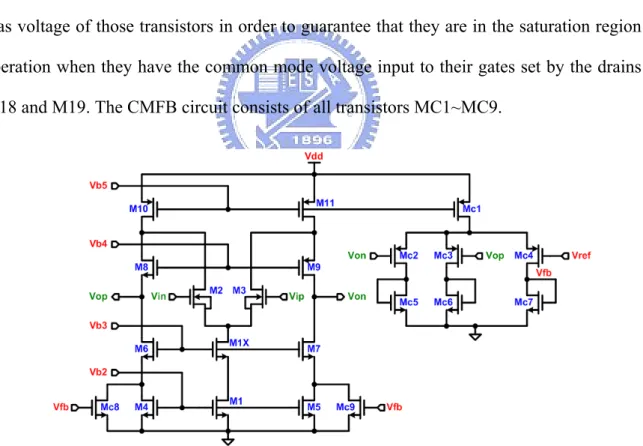
Most Sigma-delta modulator implementations have switched-capacitor integrators often using folded-csacode OTA, because of their fast settling. The dc gain of op-amps in a MOS technology intended for switched-capacitor circuits is typically on the order of 40 to 80 dB. Low dc gains affect the coefficient accuracy of the discrete-time transfer function of a switched-capacitor. The unity-gain frequency and phase margin of an OPAMP gives an indication of the small signal settling behavior of an OPAMP. A general rule is that the clock frequency should be at least five times lower in frequency than the unity-gain frequency of the OPAMP assuming little slew-rate behavior occurs and the phase margin is greater than 60 degrees.[8] Since the loads of these OPAMPs are purely capacitive (never resistive), fully differential OTA structure with gain boosting CMFB is preferred since this structure has a good high frequency power supply and common mode rejection that is essential to attenuate disturbances generated by digital parts. For this structure, the dominant pole is generated by the capacitive loaded output stage, whereas the other poles are located at relatively high frequencies [12]. The SC OPAMP is shown in Fig. 14.
Fig. 14 Fully differential gain boosting CMFB OPAMP
The use of a PMOS differential pair eliminates need of chopper stabilization, since the 1/f noise is 30 times lower than NMOS in this process. In addition, dynamic threshold variation due to charge trapping in the MOS channel is ten times less severe for PMOS [13]. Insufficient dc gain will cause integrator gain and pole error and will increase quantization noise leakage. Fully differential gain enhancement [14] is employed to increase output impedance of the cascade loads, which enhances both dc gain and power supply rejection ratio [6].
For high gain designs, two-stage configuration might be the appropriate choice; however, the speed of this configuration is the bottleneck. In this design, a fully differential folded csacode that has two fully differential folded cascade boosting amplifiers has been chosen. It has a switched capacitor CMFB circuit that will enable the OPAMP to have a common mode output voltage. The boosting amplifiers have a continuous time CMFB circuits. The boosting amplifiers are of two types [15]: the BN has a NMOS differential input stage, while the BP has a PMOS differential input stage. As shown in Fig. 14, the inputs of the BN boosting amplifier comes from the drains of M18 and M19 transistors, which are supposed to
be biased in the saturation region and have a drain-to-source voltage, Vds<0.5V. This means
that the inputs to the differential pair of BN are going to be around 2.5v, hence an NMOS differential input stage is required. The bottom boosting amplifier, BP, has its inputs coming from the drains of M8 and M9 which are supposed to be biased at Vds<-0.5V, hence a PMOS
differential input stage is required. The main OPAMP has a switched capacitor CMFB circuit in order to maximize the output range of the main OPAMP. Next, the design of the boosting amplifier is described first.
The design of the Boosting Amplifier. [14]
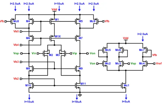
The NMOS type boosting amplifier, BN, which is continuous time common mode feedback circuit is shown in Fig. 15. Cascading the two transistors will decrease the excess bias voltage of those transistors in order to guarantee that they are in the saturation region of operation when they have the common mode voltage input to their gates set by the drains of M18 and M19. The CMFB circuit consists of all transistors MC1~MC9.
Fig. 15 NMOS-input fully differential gain boosting amplifier with continuous time CMFB The BP boosting amplifier is the same as the NMOS type with the exception that a PMOS differential input stage is used in addition to a NMOS CMFB circuit instead of the PMOS one used above. The BP boosting amplifier is shown as Fig. 16.
Fig. 16 PMOS-input fully differential gain boosting amplifier with continuous time CMFB CMFB circuit design of the boosting amplifier.
Designing the CMFB circuit of the boosting amplifiers is a straightforward process. The output of each boosting amplifier does not need high swing, thus, a continuous time CMFB circuit is used [16]. The first step is to design the boosting amplifier without the CMFB circuit such that the common mode output of the OPAMP is around BPC. Once this is
finished, part of the output is generated by the CMFB circuit using transistors MC8 and MC9. For example, suppose that after designing the OPAMP without the CMFB circuit, the channel width of M4 and M5 is 10µm for 5µA current mirror. If we assume that half output current will be provided by the CMFB circuit, then channel width of M4 and M5 will be reduced to 5µm. If Vref equals the common mode voltage of Von and Vop, then MC2-MC7 are designed such that the current in MC4 is the same as the current through both of MC2 and MC3. This means that the current through MC4 is half of the current MC1. Since the current in the path of M9 and M7 will is 1/2 of M11, then the current of MC4 is 1/2 of that in M9 or M7. So, 1/2 of the current of M9 or M7 will be provided by the CMFB circuit, and the rest is provided by M5 which will be 1/2 of the current. This is why channel width of M5 was reduced from
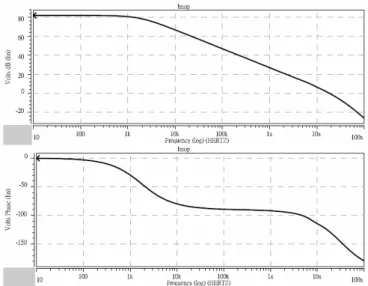
10µm to 5µm. Fig. 17 shows the AC frequency response of BN boosting amplifier. The gain is about 82dB (typical case) and phase margin is about 55 degree.
Fig. 17 Gain and phase margin with AC response of the boosting amplifier The design of the gain boosting CMFB amplifier.
Consider the simple cascade in Fig. 18(a), whose output impedance is given by
2 2 1 out m O O
R =g r r . As far as Rout is concerned, M1 operates as a degeneration resistor in Fig.
18(b), sensing the output current and converting it to a voltage. Illustrated in Fig. 18(c), the idea is to drive the gate of M2 by an amplifier that forces Vx to be equal to Vb. Thus, voltage
variations at the drain of M2 now affect Vx to a lesser extent because A1 “regulates” this
voltage. With smaller variations at X, the current through rO1 and hence the output current
remain more constant than those in Fig. 18(b), yield a higher output impedance.[17]
1 2 2 out m O O1
R ≈ A g r r (24)
concluding that Rout can be “boosted” substantially without stacking more cascode devices on
top of M2. So the Rout in Fig. 14 can be written as BN 13 13 19// BP 11 11 9
out m O O m O O
R ≈ A g r r A g r r (25)
The gain of boosting amplifier is about 80dB in Fig. 17, this is said that the gain boosting structure improve the output impedance about 10000 times. The output impedance is up to
472.7MΩ by Hspice simulation.
Fig. 18 Increasing the output impedance by feedback.[17]
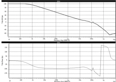
The most important part of the gain boosting CMFB OPAMP is its common-mode feedback circuit. It is a compound by switched capacitor circuit and a continuous time CMFB circuit as shown in Fig. 14. The switched capacitor CMFB circuit is utilized in order to keep the common mode output voltage at the required level while maximizing the output swing of the operational amplifier. The sizes of the switches should also be chosen carefully so that they will not have charge injection effect on the capacitors. Fig. 19 shows the AC frequency response of main amplifier. The gain is about 100dB (typical case) and phase margin is about 60 degree. Most important thing is that the unity gain frequency is up to almost about 100MHz.
3.1.2 Integrator
In order to show the new proposed MASH that can improve SNR with mismatch effect, both conventional and new proposed MASH is placed in this chip. All the circuits are based on first-order Sigma-delta modulator which is shown in Fig. 20.
Fig. 20 Basic first-order Sigma-delta modulator
While the circuit seen so far have all been shown with single-ended signals, in most analog applications it is desirable to keep the signal fully differential. Fully differential signals imply that the difference between two lines represents the signal component, and thus any noise which appears as a common-mode signal on those two lines does not affect the signal. Fully differential circuits should also be balanced, implying that the differential signals operate symmetrically around a dc common-mode voltage (the common-mode voltage is set to vdd/2). Fully differential circuits have the additional benefit that if each single-ended signal is distorted symmetrically around the common-mode voltage, the differential signal will have only odd-order distortion terms (which are often much smaller).[8] A fully differential realization of the first-order Sigma-delta modulator is shown in Fig. 21. Note here that the fully differential version is essentially two copies of the single-ended version, which might lead one to believe that it would consume twice the amount of integrated area. Fortunately, the increased area penalty is not that high. First, we see that only one OPAMP is needed although it does require extra common-mode feedback circuit. Second, note that the input and output signal swings have now been doubled size. Thus, to maintain the same dynamic range due to (kT)/C noise, the capacitors in fully differential version can be half the size of those in
the single-ended case. Since smaller capacitors can be used, the switch size widths may also be reduced to meet the same settling-time requirement. However, the fully differential circuit has more switches and wiring so this circuit will be somewhat larger than its single-ended counterpart. However, recall that the fully differential circuit has the advantages of rejecting much more common-mode noise signals as well as having better distortion performance.
Fig. 21 Fully differential first-order integrator
The basic first-order Sigma-delta modulator is composed by two components: Integrator and quantizer. The integrator is the most important part of the modulator. To get better performance, the high performance folded-cascode CMOS OPAMP is adopted in the design. [18]
Fig. 20 shows the first integrator of the first stage with the 1-b digital-to-analog converter (DAC), and Fig. 22 shows the clock timing. A parasitic-insensitive integrator (Stray-insensitive integrator) is considered to be used for high-accuracy integrated circuits. [8][19]
Even with single-ended sampling, the reference will still see data-dependent loading during the sample phase (φ1 and φ1D high). Since data dependency across CR1 remains after
the integrate phase, the reference will see a data-dependent load when recharging CR1 during
the sample phase. To avoid this mechanism, four-phase non-overlapping clock scheme was developed [6]. The difference from the conventional four-phase clock [20] is the clock sequence after the integrate phase, i.e., φ1 rising prior to φ2dD falling. This gives a short period
where both terminals of CR1 are connected to VCM. This period will discharge (“de-load”) any
data dependency across CR1 before charging the reference voltage at the next sample phase.
Another important circuit element in switched-capacitor circuits is the MOS switch. The simplest realization of an on-off switch Fig. 23(a) in MOS technology is a single MOSFET Fig. 23(b). When the gate has a sufficiently high voltage of the appropriate polarity (positive for NMOS, negative for PMOS), the switch will be “on”, and a current iD will flow
between node 1 and node 2 in response to a potential difference vDS between these node.
Since the on-value of the gate voltage vφ, derived from a clock Fig. 23(c), is usually large, it
can be assumed that the FET switch is in its linear region. A “clock feedthrough” noise will be generated.
In most applications, noise voltages of such magnitude are not tolerable. To compensate for the clock feedthrough effect using both NMOS and PMOS transistors are available. The circuit of Fig. 23(a), which compensates feedthroughs to both nodes 1 and 2, can be used. This circuit also reduces the voltage drop across the switch, and thus increases the dynamic range since smaller signals may be used [19]. The on-resistance Ron performance
of NMOS, PMOS, and CMOS switches is discussed now. For a n-channel device with the processing parameters given in the figure and a gate voltage of VDD=5v, the switch will cut
off when the signal voltage exceeds 2V. Similarly, the PMOS switch cuts off when Vin<0. The first-order Sigma-delta modulator has a feedback loop with 1-b DAC. Fig. 24 shows the transfer function of non-inverting and inverting integrator. We can only exchange the clock φ1 and φ2 to the switches which are on the feedback loop. Hence, a simple 1-b DAC
can be designed by this approach.
Fig. 24 First-order A/D modulator: [8]
(block diagram and switched-capacitor implementation)
New proposed MASH employs the time-division concept for architecture. The time- and capacitor- multiplexing switched-capacitor integrator is mention in chapter 2.
3.1.3 Quantizer
The second major component of modulator is the quantizer. The 1-bit quantizer of the modulator can be realized with a comparator. Three principle design parameters of this comparator are speed, which must be adequate to achieve the desired sampling rate, hysteresis and a latch control by clock which can hold data when in integration state.
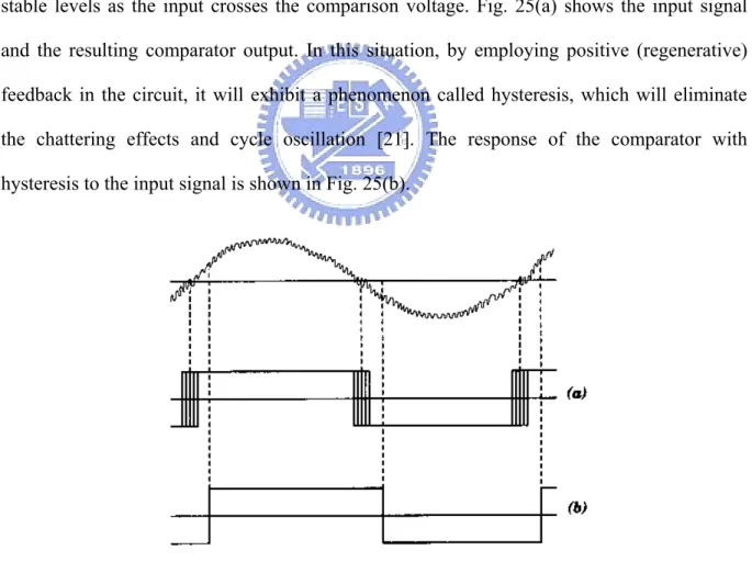
Often, comparators are used to convert a very slowly varying input signal into an output with abrupt edge, or they are used in a noisy environment to detect an input signal crossing a threshold level. If the response time of the comparator is much faster than the variation of the input signal around the threshold level, the output will chatter around the two stable levels as the input crosses the comparison voltage. Fig. 25(a) shows the input signal and the resulting comparator output. In this situation, by employing positive (regenerative) feedback in the circuit, it will exhibit a phenomenon called hysteresis, which will eliminate the chattering effects and cycle oscillation [21]. The response of the comparator with hysteresis to the input signal is shown in Fig. 25(b).
Fig. 25 Response of a fast comparator (a) without hysteresis (b) with hysteresis To combine the sample-and-hold function and the comparator function in a quantizer, I choice the source-coupled differential pair with positive feedback for hysteresis. Consider
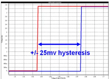
the circuit of Fig. 26, Vin and Vip are connected to the differential outputs of integrator. Suppose Vip is larger than Vin, M36 is on and M35 is off and all the tail current flows through M36 and M39. The current through transistors M35, M38, M42 and M43 are zero and the node voltage V(out) is low. Next assume that the input voltage Vip is gradually decreased and Vin is gradually increased so that transistor M35 begins conducting and part of the tail current start flowing through it. This process continues until the current in transistor M35 equals the current in M43. Any increase of the input voltage beyond this point will cause the comparator to switch state so that M36 turn off and all the tail current flows through M35. The complete schematic of a comparator with hysteresis, which consists of a source-coupled differential pair with positive feedback, is shown in Fig. 26. For this circuit the value of α is greater than 1 [22] and the simulation result with 25mV (typical) hysteresis is shown in Fig. 27.
(
)
(
)
M43M39(
(
)
)
M42M38 W/L W/L = = W/L W/L α >1 for hysteresis. (26)The gain of comparator which can be read in Fig. 27 is about3.3v=3300
1mv , or 70dB. And the propagation delay of the comparator is 5ns.
Fig. 27 The .DC simulation result of latch comparator with hysteresis
Fig. 28 The .Tran simulation result of latch comparator with hysteresis
3.2 Digital circuit realization
The digital circuits include non-overlapping four-phase clock generator, feedback loop control circuit with a 20% mismatch signal externally, digital delay circuit and other circuit for new proposed MASH only.
3.2.1 Switched-capacitor implementation and C-ratio mismatch control
The basic switching capacitor circuit in integrator has been described in section 3.1.2. Now, the digital control parts of switching capacitor implementation will be discussed in this
section. First, we talk about the four-phase non-overlapping clock generation circuit. Fig. 22(b) is the output waveform of four-phase clock. This circuit is based on two phase non-overlapping clock generation circuit. At least one pair of non-overlapping clock is essential in switched-capacitor circuits. These clocks determine when charge transfers occurs and they must be non-overlapping in order to guarantee charge is not inadvertently lost. As seen in Fig. 29(a), the term non-overlapping clocks refers to two logic signals running at the same frequency and arranged in such a way that at no time are both signal high. Note that the time axis in Fig. 29(a) has been normalized with respect to the clock period, T. Such normalization illustrates the location of the sample numbers of the discrete-time signals that occur in switched-capacitor filters. As a convention, we denote the sampling numbers to be integer values just before the end of clock phase φ1, while the end of clock φ2 is deemed to be
1/2 sample off the integer values as shown. However, it should be noted that it is not important that the falling clock edge of φ2 occur precisely one-half a clock period earlier than
falling edge of φ1. In general, the locations of the clock edges of φ1 and φ2 need only be
moderately controlled to allow for complete charge settling. So in four-phase clock, a new stage of “de-load” is applied to discharge the sampling capacitor Cs which has been described in previous section 3.1.2.
One simple method for generating non-overlapping clocks is shown in Fig. 29(b). Here, delay blocks are used to ensure that the clock remain non-overlapping. These delays could be implemented as a cascade of an even number of inverters.
The final four-phase non-overlapping clock generation circuit is shown in Fig. 30. The delay unit is composed by two long channel (3µm) inverters which are shown in Fig. 29(b). Note that every output has its buffer to drive the MOS switches.
Fig. 30 The schematic of four-phase non-overlapping clock generation
Fig. 31 The simulation result of four-phase non-overlapping clock generation
The control circuit as shown in Fig. 32 is another key block to maintain the function of Sigma-delta modulator. The node of “In” is the output of quantizer, it is a digital signal. The output of quantizer is connected to the input of DAC in feedback loop. In order to feed the control signal to DAC, this control circuit must be able to fit the function of non-inverting integrator or inverting integrator which have explained in section 3.1.2.
Fig. 32 The schematic of control circuit The brief function is list below:
CTL1=CLK1; CTL2=CLK2 when IN=H (27) CTL1=CLK2; CTL2=CLK1 when IN=L (28) We can easily know that the φ1 and φ2 will change the polarity when IN is switched.
Review the Fig. 24, the DAC function is applied by non-inverting and inverting integrator, and the value of reference voltage can adjust the feedback volume of DAC. Finally sum the input signal and feedback value of DAC by superposition which is shown in Fig. 24.
The major issue of this thesis is reducing the effect with mismatch errors. The non-linear of OPAMP is not easy to establish by external signal, but capacitor ratio mismatch is much easier to construct with an external signal-“MIS”. A C-ratio mismatch is forced when “MIS” pin is connected to “H”. The design value of capacitor in feedback DAC is 1p in normal (match) condition. This 1p capacitor is divided into two parts, 0.8p and 0.2p. The control signals CTL1, ZCTL1, CTL2 & ZCTL2 in Fig. 32 are connected to 0.8p capacitors; and CTL1_M, ZCTL1_M, CTL2_M & ZCTL2_M in Fig. 32 are connected to 0.2p capacitors. 0.8p+0.2p capacitors are used in normal (match) condition, but only 0.8p capacitor is used in mismatch condition, so a 20% mismatch happen. The SNR can be measured by switching the
“MIS” pin, and compare the value between match and mismatch. The expectative result is that the SNR of conventional MASH will descend with “MIS” is “H”. And only a little SNR will drop in new proposed MASH whether “MIS” is “H” or “L”. Here the “MIS” control must be added in this control circuit, and the simulation result is shown in Fig. 33.
Fig. 33 The simulation result of control circuit
Finally, the conclusion of control circuit with mismatch function is list below: CTL1=CLK1; CTL2=CLK2 when IN=H (29) CTL1=CLK2; CTL2=CLK1 when IN=L (30) CTL1=”L”; CTL2=”L” when MIS=H (31) CTL1=CTL1_M; CTL2=CTL2_M when MIS=L (32)
3.2.2 Logic circuit and digital cancellation
In this section, I would like to introduce the extra circuits which are used in new proposed MASH. They include the integrator capacitors which share sampling capacitors and op-amps, digital delay circuits and new clock generator. The first part has been mentioned in
chapter 2.3. In order to keep the sampling frequency, the clock frequency of new proposed MASH is the double of conventional MASH. So each sampling is formed with two clocks. Both Sigma-delta modulators are first-order ones which are connected to input signal in first clock period, in other word the input signal is sent to both Sigma-delta modulators at the same time, and then be second-order Sigma-delta modulators which are connected to other side Sigma-delta modulator in second clock period. The first and second period data must be keep in integrator capacitor. This is why we need two capacitors for new proposed MASH. Only one more capacitor is added as conventional MASH, the sampling capacitors and op-amps can be shared.
The clock generation circuit is the other block which is added in new proposed MASH. In order to divide the clock for time- and capacitor- multiplexing, all kinds of clocks must be generated to re-locate the data path. Fig. 34 shows a non-overlapping clock divide one sampling frequency into two stages: timing phase-1 and timing phase-2. The brief principle of this circuit is introduced in chapter 3.2. Here the outputs of the two stage clocks, clk1 and clk2, will be produced other control clocks in Fig. 35 which is like a counter by 2 circuit. These control clocks are the key signals to re-locate the data path to be a new proposed MASH.
Fig. 35 Clock generation circuit for new proposed MASH
The digital delay circuit of z-1 and z-1/2 are approached by a simply flip-flop cell which is shown in Fig. 36(a) and (b). The z-1 mean that the digital data is delayed one sampling clock (equal to two input clocks), and the z-1/2 mean that the data is delayed half sampling clock (equal to one input clock). This is because the time has z-1/2 difference between first-order Sigma-delta modulator and second-order Sigma-delta modulator. So both z-1 and z-1/2 are necessary.
3.2.3 System design
In this section we give a design discussion of a cascaded Sigma-delta modulator (MASH). The 1-1 modulator architecture with coefficients is repeated in Fig. 37 for convenience. We start by choosing the coefficients in the modulator. The transfer function of the modulator is given by [23]
-1 2 -2 1c (1-z ) e2(z) Y(z)=z X(z)+ H (33)
where e2(z) is the quantization noise in the second stage. To make the quantization noise small, H1c should be as close as 1. This coefficient also determines the gain factors in the
digital cancellation logic. All other gain factors in the modulator are in a SC implementation determined by capacitor ratios. The capacitor ratios should be chosen such that the circuit is easy to layout using unit-capacitors.
Fig. 37 2nd-order 1-1 cascaded Sigma-delta modulator with system coefficient.
To make the modulator less sensitive to circuit noise the voltage swings in all the nodes of the circuit should be approximately the same. The maximum signal swing at the input of last stage can be determined by [24]
2 1c 1 1 x =H x + -H 2 2 ∆ ∆ ⎛ ⎜ ⎝ ⎠ ⎞ ⎟ (34)
Where ∆ is the step size in the D/A converters and x1 is the maximum swing at the input of
the first stage. To maximum H1c, H1 should be 1. The integrator gains are chosen to give
signal swings at the OPAMP’s outputs that equal to or slightly less than the swing of the feedback signals of the DAC.
Set H1=1, and choice Cs1=1p, Ci1=4p : 1 1 Cs 1p 1 K1= = Ci 4p 4 ⇒ (35) 1 B1 K1= B1=1 4 ⇒ × ⇒ (36) Set K2 equal to K1 : 1 B2 K2= B2=1 4 ⇒ × ⇒ (37) 1 H1 H1c K2= H1=H1c=1 4 ⇒ × × ⇒ (38) 2 2 2 2 Cs Cs 1 H1c K2= = Cs =4p K1 Ci 4p ⇒ × ⇒ (39)
After calculating, the capacitor sizes can now be determined as shown in Table I and Fig. 38. And the final SC-implementation of conventional 1-1 Sigma-delta modulator is shown in Fig. 39 and new proposed 1-1 Sigma-delta modulator is shown in Fig. 40. All capacitor values of both modulators are listed in table II.
Table I Gain factors in the modulator.
Coeff. Value K1 1/4 H1 1 H1c 1 K2 1/4 H2 1 H2c 1
Fig. 38 Gain factors in the modulator.
Fig. 40 SC-implementation of new proposed 1-1 modulator.
Table II Capacitor values in the modulator.
Capacitor Value(pF) Cs1 1 Ci1 4 Cβ1 1 Cs2 4 Ci2 4 Cβ2 1 Cβ3 1
3.3 Simulation
results
The simulated performance of the 1-1 MASH or cascaded architecture will now be presented. In the case of digital audio, various sampling frequencies might be fs=5.6448MHz,
2f0=44.1 kHz, which represent an oversampling ratio of 128. As discussed in 3.2, a number of
circuit imperfections cause the modulator performance to deviate from this ideal prediction. A capacitor mismatch will be simulation by Matlab Simulink to show the impact of SNR.
3.3.1 Matlab (Simulink) simulation results
The Simulink model of 1-1 modulator structure is shown in Fig. 41. Note that both of the integrators have a sampled-and-hold delay. This sampled-and-hold signal is then applied to an A/D delta-sigma modulator, which has as its output a 1-bit digital signal. This 1-bit digital signal is assumed to be linearly related to the input signal, although it includes a large amount of out-of-band quantization noise. To remove this out-of-band quantization noise, a digital decimation filter is used as shown. Conceptually, one can think of the decimation process as first reducing the quantization noise through the use of a digital low-pass filter. This decimation process does not result in any loss of information, since the bandwidth of the original signal was assumed to be f0.
Finally, it should be noted that much digital circuit complexity can be saved by combining the digital low-pass filter with the re-sampling block to directly produce the down sampled signal. It is of interest to look at what element most strongly affects the linearity of this oversampling A/D system. Setting all of the coefficients to 1, and the quantization error from the first stage is completely cancelled at the modulator output when the second order feedback DAC gain is set to 1. By changing the DAC gain, a comparison of immunity to gain mismatch effects can be simulated.
Fig. 41 The Simulink model of conventional 1-1 modulator structure
The new proposed MASH structure of Simulink diagram is shown in Fig. 42. In order to ignore the timing switch, the double number of integrators and comparators are applied in Simulink model. Note that the same number of OPAMPs and comparators are used on chip actually by using time divided technique. The (A1) and (A2) modulators are used the same OPAMPs and comparators; the (B1) and (B2) modulators are used the same OPAMPs and comparators. A sampling period is divided by timing switch into 2 section periods. The input signal is sent into (A1) and (B1) at the same time during section period 1. After integrating and quantizing, the timing is into section period 2. Let the output data of (A1) and (B1) be intercrossed, the output of (A1) is sent to (B2) and the output of (B1) is sent to (A2). The mismatch error can be compensated by intercrossing the data path, the transfer function of new proposed MASH is list below again.
Y(z)= 1 2 -2 1 2 -1
( )
-1(
)
1 -1 2 2 -1 21 2 1 2
K +K K -K K K
z X(z)+ z 1-z Q -Q + (1-z ) Q + (1-z ) Q
2 2 2 ′ 2 ′ (40)
The first order quantization error can be minimum by (K1-K2)×(Q1-Q2) which have
Fig. 42 The Simulink model of new proposed 1-1 modulator structure
The Matlab (Simulink) simulation results between conventional MASH and new proposed MASH is shown in Fig. 43 and Fig. 44. The mismatch errors have rise the noise floor and reduced the SNR in conventional MASH which is shown in Fig. 43(b). Let’s take a look at Fig. 44, just a little difference can be found. A successful result is proved that the new proposed MASH can suppress the SNR degradation with mismatch effect.
Fig. 43 The Simulink simulation results of conventional MASH (a).No mismatch (b).With 20% mismatch
Fig. 44 The Simulink simulation results of new proposed MASH (a).No mismatch (b).With 20% mismatch
The comparison of immunity to mismatch effect with all kinds of structure is depicted in Fig. 45. An interesting thing is happened in the simulation results of new proposed MASH. The SNR is better with a little mismatch. Due to it is supposed that no any variance is produced by behavior simulation. Another inference is proposed here and the transfer function must be list again.
Fig. 45 The Simulink simulation results between different mismatch (Comparison of immunity to mismatch effects)[3]
Y(z)= 1 2 -2 1 2 -1
( )
-1(
)
1 -1 2 2 -1 21 2 1 2
K +K K -K K K
z X(z)+ z 1-z Q -Q + (1-z ) Q + (1-z ) Q
The first-order quantization errors have been discussed in previous chapter. Now the second-order quantization errors are focused. We know that quantization error have two directions (+ and -) based on original signal, and the phase of quantization error is signal dependant. It can supposed that Q1 and Q2 are same phase due to the two modulators have the
same input signal, but Q1’ and Q2’ can not be supposed to be the same phase. This is said that
Q1’ and Q2’ have opposite direction in some case. When this case happened, better SNR can
be found which is depicted in Fig. 45.
3.3.2 Hspice simulation results
After behavior simulation by Matlab Simulink, it is proved that the new proposed MASH has immunity to mismatch effects. The Hspice simulation results by circuit achievement are discussed here. Only modulator part is implemented to the chip, because decimator part can be done by DSP processor. The plan of this chip is only PCM (pulse code modulation) data output then calculate output data by Matlab (including math calculation of digital cancellation and plot the spectrum by FFT then measure SNR finally).
Note that the system simulation need a long time by transition Hspice simulation, and the accurate option is also a key element to get better SNR. In order to shorten the simulation time, only the worse case is simulated in Hspice simulation by a few FFT points in spectrum. The signal bandwidth is 22.05 kHz for 44.1 kHz Nyquist rate which is applied by MP3 coding. The clock is 5.6448MHz for OSR (oversampling ratio) is 128. The calculation of SNR is specified the signal bandwidth without any weighting filter by Matlab.
A 20% area mismatch of capacitor is placed in feedback loop DAC on purpose. An external signal can switch it from 20% mismatch to no mismatch. We can compare the mismatch effect by the measurement on chip.
Finally, the simulation results are summarized in Table III, and the specification is list as Table IV.
Table III Summary of simulation results
Pre-Sim Post-Sim
Conventional MASH(No mismatch) 78.9310 dB 75.1694 dB
Conventional MASH(20% mismatch) 74.6885 dB 70.4242 dB
New MASH(No mismatch) 78.5209 dB 75.2846 dB
New MASH(20% mismatch) 78.4780 dB 74.5603 dB
Table IV Summary of specification
Technology TSMC 0.35um 2P4M Supply voltage Vdd=DVdd=IOVdd=3v
Bandwidth 22.05kHz Power Dissipation conventional=3.94mw
new proposed=5.38mw Transistor/Gate count 1176
Chip area conventional MASH (600µm×1500µm) new proposed MASH (700µm×1500µm) Oversampling ratio 128
CHAPTER 4
Experimental results
The second-order MASH modulator has been fabricated in a 0.35µm CMOS technology with poly-to-poly capacitors. The total chip size of the converter was 2mm × 2mm (the chip area of conventional MASH is 600µm×1500µm; and new proposed MASH is 700µm×1500µm). The upper side of the chip which is shown in Fig. 46 is conventional MASH, and the lower side of the chip is new proposed MASH. The new proposed MASH need extra logic circuit to control switch to re-locate data path, but just a little larger than conventional MASH. In other word, almost the same chip area is needed for new proposed MASH to implement the immunity of gain mismatch effects.
4.1 Layout
descriptions
On this chip containing OPAMPs, switches, and capacitors, it is usually efficient to arrange these components in separate areas on the chip. Thus, all OPAMPs may occupy one row, all capacitors a second one, and all switches a third, with the supply and clock lines running in parallel along the edges. This is in order to prevent noise injection from the power, ground, and the clock lines, two precautions of equal importance must be observed. First, these must, as far as possible, be kept free from noise. Second, the noise coupling from the lines into the signal path should be minimized. The first requirement is especially important if the chip contains both analog and digital circuitry which is separated by capacitors in this chip. Besides, using separated (“dedicated”) power lines for the analog and digital circuitry to suppress the analog supply noise. Further improvement can be achieved by using also separate bonding pads for these dedicated lines, using separate pins as well (AVdd, DVdd and IOVdd are used here), which are short-circuited externally. Using external decoupling capacitors at the pins, this residual impedance can be reduced to a very low value and the spike noise essentially eliminated. Under these circumstances, the bias voltage lines for the substrates can also be connected to the analog supply pads without introducing any digital noise into the substrate. These substrate bias lines must have as many contacts (pick-up) to the substrate (or well) as possible. These contacts will collect the electrons or holes injected into the substrate (or well), keep the substrate (or well) at a fixed potential, and will thus prevent the occurrence of latch-up, a fatal problem which can affect CMOS integrated circuits. To prevent latch-up, A guard ring structure with NW pseudo-collector and P+ pickup is inserted in between I/O buffer and internal circuit area which is shown in Fig. 46.
A highly linear capacitance in an integrated circuit is typically constructed between two polysilicon layers in TSMC 0.35µm technology, as shown in Fig. 47. These capacitors are known as double-poly capacitors. The thin oxide is an insulating layer separating the two
relatively conductive polysilicon layers, while the thick oxide is also an insulating layer but of much thicker width. The desired capacitance, C1, is formed as the intersection of area between
the two polysilicon layers, poly1 and poly2. However, since the substrate below the poly2 layer is an ac ground (the substrate is connected to analog ground), there also exists a substantial parasitic capacitance, Cp2, which may be large as 20 percent of C1.
Fig. 47 A double-poly capacitor
Because the bottom plate is often explicitly shown to indicate that a larger parasitic capacitance occurs on that node, the parasitic-insensitive integrator is applied in this chip which is shown in Fig. 48. Note that Cp1 and Cp4 have larger capacitance while they are the
bottom plate. It does not affect the circuit operation due to more driving to these nodes, so the top plate of PIP capacitors must be connected to the input of OPAMPs on chip layout.
![Fig. 12 Time- and capacitor- multiplexing switched-capacitor integrator [3]](https://thumb-ap.123doks.com/thumbv2/9libinfo/8750330.205782/27.892.283.669.413.686/fig-time-capacitor-multiplexing-switched-capacitor-integrator.webp)