國立交通大學
電子工程學系 電子研究所碩士班
碩士論文
適用於可攜式腦心監護系統之高能源效率與高整合
8 通道前端類比電路
A Power-Efficient and High-Integrated 8-Channel Front-End IC for
Portable Brain-Heart Monitoring
研 究 生 : 蔡宗翰
指導教授: 方偉騏 教授
適用於可攜式腦心監護系統之高能源效率與高整合
8 通道前端類比電路
A Power-Efficient and High-Integrated 8-Channel Front-End IC for
Portable Brain-Heart Monitoring
國立交通大學
電子工程學系 電子研究所碩士班
碩士論文
A Thesis
Submitted to Department of Electronics Engineering & Institute of Electronics College of Electrical and Computer Engineering
National Chiao Tung University In partial Fulfillment of the Requirements
for the Degree of Master of Science
in
Electronics Engineering December 2011
Hsinchu, Taiwan, Republic of China
中 華 民 國 一 ○ ○ 年 十 二 月
研究生:
蔡宗翰
Student :
Chung-Han Tsai
i
適用於可攜式腦心監護系統之高能源效率與高整合
8 通道前端類比電路
學生:蔡宗翰 指導教授:方偉騏 教授 國立交通大學電子工程學系 電子研究所碩士班 中文摘要 近年來老年人口比例快速增加,全球年齡超過六十五歲以上的人口預計在 2025 年會達到 7.61 億人口。這樣會使社會邁入老年化且會造成醫療照顧等相關 問題。因此整合型可攜式照護系統的相關研究成為已經成為近年來的重要課題。 本論文中提出一種針對處理多種訊號包括腦電訊號(EEG)、心電訊號(ECG) 和擴散光學腦部影像重建(DOT)所構成之低功耗高整合型感測電路雛型設計, 藉此以推動整合型可攜式醫療照護系統的發展。 由於生理電訊號非常微弱,為了使其可以正常被觀察及應用,因此在系統設 計上必須準確且不失真地放大該訊號。此微弱的生理電訊號相當容易受外在雜訊 干擾,因此在設計上,必須有效減少雜訊造成的影響,而每個生理訊號的電壓範 圍不一樣,也必須用不同的方式萃取出來。最後,為了進行即時訊號處理及運用, 因此必須把類比訊號轉換成數位訊號。而要把多個設計整合在單晶片中且符合高 能源效率及高整合度等可攜式儀器的要求,這就是此整合型晶片主要的難度及貢 獻。本論文所提出之 Chopper Differential Difference Amplifier, Adjustable Gain Amplifier, Adjustable Bandwidth Low Pass Filter and Successive Approximation Registers Analog-to-Digital Converter 皆為達此目的所設計。最後此前端電路將會
ii 被使用擷取訊號傳給後端作訊號處理,進一步達到更多功能的生醫系統監測晶片。 最後,本論文所提出之多通道高整合型與高能源效率之前端類比電路已被設計並 透過台積電 180 奈米製程下線並完成測試。 關鍵字:腦電訊號、心電訊號、擴散式光學影像重建、整合型生醫系統、可攜式 系統、前端類比電路
iii
A Power-Efficient and High-Integrated 8-Channels Front-End IC for
Portable Brain-Heart Monitoring
Student:
Chung-Han Tsai
Advisor:
Wai-Chi Fang
Department of Electronics Engineering and Institute of Electronics
National Chiao Tung University
Abstract
Proportion aging is increasing rapidly in recent years. The worldwide population of people over the age of 65 has been predicted to become 761 million in this year 2025. Hence, the aging society will have a great demand of health-care system for elders, especially an integrated portable one. In this thesis, a preliminary design of high-integrated and low power consumption for processing multi signals such as electroencephalogram (EEG)signal, electrocardiogram (ECG)signal and diffuse optical tomography (DOT)is presented. The significance of this system is to enable the practical development of integrated portable health-care system for brain-heart monitoring.
As the biomedical signals are weak, it is necessary to amply them for accurate monitoring. The weak biomedical signals are easily affected by external noise, so the circuit has to reduce the inference of noises. The different biomedical signals have different amplitudes and different bandwidths. Therefore, the circuit also has to deal with these problems. Finally, the biomedical signals are analog signals, but the signals are not only for monitoring but also for signals processing for the most urgent treatment conveniently. So, the analog-to-digital converter cannot be avoided. In other words, it is difficult to integrate these designs on a chip for portable health-care
iv
system. To solve this problem, Chopper Differential Difference Amplifier, Adjustable Gain Amplifier, Adjustable Bandwidth Low Pass Filter and Successive Approximation Registers Analog-to-Digital Converter are presented in this thesis. Finally, the results from this front-end circuit will convey to back-end for digital signal processing to achieve the multi-capability biomedical system monitoring chip. This multi-channel, high integrated and low power consumption has been implemented using TSMC 180 nm CMOS Mixed Signal RF General Purpose Standard Process.
Keywords:EEG, ECG, Diffuse Optical Tomography, Integrated Health-Care System,
v
誌謝
在碩士班的求學過程中,除了學到許多的研究方法與專業知識外,更重要的 是學習到正確研究態度。如何從不懂與錯誤中學習與凡是不僅盡心盡力更要小心 仔細是十分重要的。我想在此感謝我的指導教授方偉騏教授在研究上的指導,不 只交會我專業知識更十分耐心的引導我從未知的領域中找到出路。也感謝國立交 通大學提供給我如此優良的學習環境,真的很榮幸能成為國立交通大學電子所的 一員。 能夠完成此論文都要感謝我的指導教授方偉騏教授,謝謝方老師特地從 NASA 回來母校從事教職。方老師提不只提供了理想的研究環境與豐富資源,更 能提供許多專業的人才可供我詢問專業領域的問題。而且在方老師的指導下,不 僅專業領域上的研究,也可學習到如何與別人合作的重要團體合作技巧。另外我 要感謝我的口試委員陳科宏教授與黃祥哲教授,有了他們的建議使我的論文更能 完善。 同時也感謝實驗室中的學長與學弟,謝宗翰學長常教導我研究上不懂之處, 許多心得也是與宗翰學長討論中而得到,實在是讓我學習許多。亦仲學弟也幫忙 了我許多研究方面的事情,有了這兩位學長與學弟我的研究論文才能如此完整的 呈現。當然,實驗室中其他的學弟們:康適、世揚、偉業、佳慶、敬儒、奕仲、 瑞傑、子訓、冠儒、坤智,在學習中也提供了非常大的幫忙。如果之後有需要我 幫忙的地方,我也一定回盡全力幫忙。 最後要感謝我的爸爸、媽媽與妹妹所給予的支持與關心使我能在研究時沒有 後顧之憂,我才能用這麼多的時間渡過所有難關。 謹以本論文獻給我的家人及所有關心我的師長、同學與朋友們。vi
Table of Contents
中文摘要 ……….i Abstract ………..…….…iii 誌謝 ………...…v Table of Contents………...……..vi List of Figures……….………...viii List of Tables………..xiii Charter 1 Introduction………..11.1 Healthcare System and Three Common Biomedical Systems…….……...1
1.1.1 Electroencephalogram………2
1.1.2 Electrocardiogram………..4
1.1.3 Near-Infrared Spectrogram on Human Tissue………8
1.2 The Important Development of HealthCare System………...9
1.3 The Solution of Highly Integrated Healthcare System……….11
1.4 Contribution of This Work………...……...11
1.5 Organization of The Thesis………..…12
Chapter 2 8-Channel Analog Front-End IC………...13
2.1 The Architecture of 8-channel Analog Front-End IC………...15
2.2 Chopper Differential Difference Amplifier………...16
2.3 Operation Amplifier……….…29
2.4 Adjustable Gain Amplifier………...36
2.5 Adjustable Bandwidth Low Pass Filter………...38
2.6 Notch Filter………..41
2.7 The Architecture of One Signal Channel ………...43
2.8 The delay of Front-End Circuit………...44
vii
2.10 8-to-1 Multiplexer………47
2.11 The Architecture of SAR-ADC………....49
2.11.1 Introduction to ADC……….………49
2.11.2 Successive Approximation Register Analog to Digital Converter………..…53
2.11.3 Track-and-Hold Circuit………...53
2.11.4 Comparator………...…55
2.11.5 Digital-to-Analog Converter………...56
2.11.6 Successive Approximation Register……….57
2.11.7 Simulation of SAR-ADC………...59 2.12 Chip Implementation………67 2.12.1 Chip Layout………..………....67 2.12.2 Package Layout………68 2.12.3 Expected Specification……….68 2.12.4 Die Photo………...69
Chapter 3 Measurement Environment and Result………70
3.1 8-channel Front-End Circuit………...70
3.2 SAR-ADC………...75
3.3 Comparisons with Other Work……….80
Chapter 4 Revised Architectures………...81
Chapter 5 Conclusion and Future Work………83
5.1 Conclusion………....83
5.2 Future Work………..85
viii
List of Figures
Figure 1.1 The structure of brain………...2
Figure 1.2 The normal ECG wave………...5
Figure 1.3 The theory of ECG generated………...6
Figure 1.4 The architecture of portable real-time diagnostic system………10
Figure 2.1 The architecture of 8-channel front-end IC………..13
Figure 2.2 The architecture of one channel………...13
Figure 2.3 The system overview of front-end IC connect to 3 in 1 IC…………..14
Figure 2.4 Portable brain-heart monitoring system overview………...16
Figure 2.5 The circuit of chopper differential difference amplifier………...18
Figure 2.6 The circuit of chopper technology………19
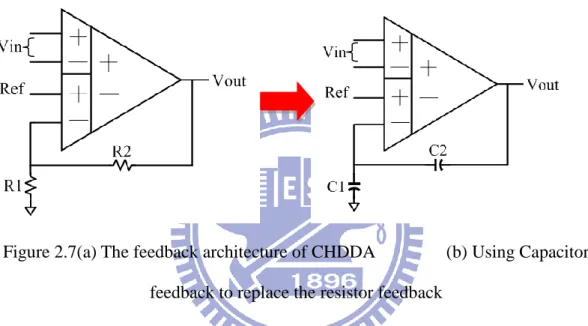
Figure 2.7 (a) The feedback architecture of CHDDA (b) Using Capacitor feedback to replace the resistor feedback……….19
Figure 2.8 The control circuit of impendent reference voltage………...21
Figure 2.9 The circuit of chopper technology………21
Figure 2.10 Frequency response (a) Pre-Layout-simulation (b) Post-layout-simulation………22
Figure 2.11 Common-mode rejection ratios (CMRR) (a) Pre-Layout-simulation (b) Post-layout-simulation………22
Figure 2.12 Input common-mode range (ICMR) (a) Pre-Layout-simulation (b) Post-layout-simulation………23
Figure 2.13 Slew rate (SR) (a) Pre-Layout-simulation (b) Post-layout-simulation.23 Figure 2.14 Input noise (a) Pre-Layout-simulation (b) Post-layout-simulation…..23
Figure 2.15 Function simulation of CHDDA (a) Pre-Layout-simulation (b) Post-layout-simulation………24
ix
Figure 2.16 Independent reference voltage of modified CHDDA………...24
Figure 2.17 Function simulation of modified CHDDA………...24
Figure 2.18 The circuit of operation amplifier………30
Figure 2.19 Frequency response (a) Pre-Layout-simulation (b) Post-layout-simulation………31
Figure 2.20 Common-mode rejection ratios (CMRR) (a) Pre-Layout-simulation (b) Post-layout-simulation………31
Figure 2.21 Input common-mode range (ICMR) (a) Pre-Layout-simulation (b) Post-layout-simulation………31
Figure 2.22 Slew rate (SR) (a) Pre-Layout-simulation (b) Post-layout-simulation.32 Figure 2.23 Noise analyses (a) Pre-Layout-simulation (b) Post-layout-simulation32 Figure 2.24 Adjustable gain amplifiers………...38
Figure 2.25 Simulation of adjustable gain amplifier (a) Pre-simulation (b) Post-simulation……….38
Figure 2.26 Sallen-Key low pass filter………39
Figure 2.27 The architecture of Switch capacitor technology……….40
Figure 2.28 Switch-capacitor low pass filter………...40
Figure 2.29 Simulation of EEG Low pass filter (a) Pre-simulation (b) Post-simulation……….41
Figure 2.30 Simulation of ECG Low pass filter (a) Pre-simulation (b) Post-simulation……….41
Figure 2.31 Notch Filter………..42
Figure 2.32 PMOS substitutes resistor………42
Figure 2.33 Modified Notch filter………...43 Figure 2.34 Simulation of Notch Filter (a) Pre-simulation (b) Post-simulation….43
x
Figure 2.35 The delay of one channel analog front-end………..44
Figure 2.36 The delay of multiplexer………..45
Figure 2.37 Sharing the same signal chain………..45
Figure 2.38 Eight same signal chain………46
Figure 2.39 Non-overlapping clock generator……….47
Figure 2.40 Non-overlapping clock……….47
Figure 2.41 Non-overlapping clock delay control………...47
Figure 2.42 8-to-1 multiplexer……….48
Figure 2.43 Transmission gate……….48
Figure 2.44 Two-Slopes ADC………..50
Figure 2.45 Sigma-Delta ADC………51
Figure 2.46 SAR-ADC………51
Figure 2.47 Cyclic ADC………..51
Figure 2.48 Pipeline ADC………52
Figure 2.49 Flash ADC………52
Figure 2.50 Two-Step ADC……….52
Figure 2.51 Time-Interleaved ADC……….53
Figure 2.52 The architecture of SAR-ADC……….53
Figure 2.53 The architecture of track-and-hold………...54
Figure 2.54 The simulation of track-and-hold……….54
Figure 2.55 The architecture of comparator………...…….55
Figure 2.56 The simulation of comparator………..55
Figure 2.57 The architecture of capacitor array………...57
Figure 2.58 The architecture of successive approximation register………57
xi
Figure 2.60 The simulation of comparator successive approximation registers…..59
Figure 2.61 The architecture of SAR-ADC……….…59
Figure 2.62 Pre-layout simulation of SAR-ADC AC analysis result ENOB……..60
Figure 2.63 Post-layout simulation of SAR-ADC AC analysis result ENOB…….60
Figure 2.64 Pre-layout simulation of SAR-ADC DC analysis result INL, DNL…61 Figure 2.65 Post-layout simulation of SAR-ADC DC analysis result INL, DNL...61
Figure 2.66 Pre-layout simulation of SAR-ADC DC Analog and Digital Function………64
Figure 2.67 Post-layout simulation of SAR-ADC DC Analog and Digital Function………65
Figure 2.68 Pre-layout simulation of SAR-ADC DC Binary Code……….65
Figure 2.69 Post-layout simulation of SAR-ADC DC Binary Code………….…..66
Figure 2.70 The chip layout of 8-channel front-end circuit……….67
Figure 2.71 The package layout of 8-channel front-end circuit………..68
Figure 2.72 The chip photo of 8-channel front-end circuit………..69
Figure 3.1 Measurement environments and machine………....71
Figure 3.2 Measurement environment and chip test board………72
Figure 3.3 The output of CHDDA……….72
Figure 3.4 The input of ADC……….73
Figure 3.5 Noise analysis………...73
Figure 3.6 The analysis of PSRR +………...74
Figure 3.7 The analysis of PSRR -………75
Figure 3.8 Agilent 93000………...75
Figure 3.9 Successive approximation register analog-to-digital………...76
xii
Figure 3.11 DNL of Successive approximation register analog-to-digital………..77 Figure 3.12 INL of Successive approximation register analog-to-digital…………78 Figure 3.13 Input and clock……….78 Figure 3.14 Output of D0~D19………79 Figure 4.1 Revised 8-channel front-end architectures………...81 Figure 4.2 Simulation of revised 8-channel front-end (a) Pre-simulation (b)
Post-simulation……….82 Figure 4.3 Layout of revised 8-channel front-end……….82 Figure 5.1 Figure 4.1 4-channel front-end extends to 64-channel front-end...………..85
xiii
List of Tables
Table 1.1 The characteristics of EEG activities………...4
Table 1.2 The characteristics of ECG activities……….6
Table 1-3 Characteristics of three main types of diffuse optical measurements……….8
Table 2.1 The sizes of transistors……….20
Table 2.2 The sizes of devices………..21
Table 2.3 0℃ Pre-Layout-Simulation………..25 Table 2.4 25℃Pre-Layout-Simulation……….26 Table 2.5 80℃ Pre-Layout-Simulation………...26 Table 2.6 0℃ Post-Layout-Simulation………...…….27 Table 2.7 25℃ Post-Layout-Simulation………..28 Table 2.8 80℃ Post-Layout-Simulation………..28
Table 2.9 The size of operation amplifier………30
Table 2.10 0℃ Pre-Layout-Simulation………..32 Table 2.11 25℃ Pre-Layout-Simulation………...33 Table 2.12 80℃ Pre-Layout-Simulation………...33 Table 2.13 0℃ Post-Layout-Simulation………...34 Table 2.14 25℃ Post-Layout-Simulation………..35 Table 2.15 80℃ Post-Layout-Simulation………..35
Table 2.16 The operation of successive approximation register………58
Table 2.17 Pre-Layout Simulation of SAR-ADC………..62
Table 2.18 Pre-Layout Simulation of the worst case of SAR-ADC………...62
Table 2.19 Post-Layout Simulation of SAR-ADC……….63
Table 2.20 Post-Layout Simulation of the worst case of SAR-ADC………….…63
xiv
Table 3.1 Front-End Specification in Simulation and Measurement…………...71 Table 3.2 Measurement Specification of SAR-ADC………...79 Table 3.3 Comparisons with Other Work……….80 Table 5.1 The specification of measurement result………..84
1
Chapter1 Introduction
In recent years, the rapid increase of the aged population is a worldwide phenomenon and the worldwide population of people over the age of 65 will even be doubled from 1990 to 2025 [1]. In Taiwan, the age of the population has risen from 26 to 36 and the population of people of ages under of 25 has been rapidly decreasing in the past twenty years [2]. This way, most of the elder suffer from chronic ailments [3] and illnesses related to central nervous system (CNS). But the proportion of dual-earner families is increasing, and these families have no time to take care the elders. Therefore, healthcare system plays an important role in the next generation.
1.1 Healthcare System and Three Common Biomedical System
It is necessary to monitor biomedical signals for a long time for a healthcare system. According to the recently studies, the most common biomedical signals for diagnosis are electroencephalogram (EEG) signals and electrocardiogram (ECG) signals. EEG signals are biomedical signals of brains and ECG signals are generated by hearts. There are many studies having shown that combined analyses of EEG and ECG are useful for better disease diagnosis. Signals from brain monitors include not only EEG signals, but also diffuse optical tomography (DOT) signals. Applications of EEG in diagnostic neurology include detection of encephalopathy such epilepsy, seizures, coma, stroke and tumors. DOT is a non-invasive imaging method popularly used to detect breast cancers and to measure blood flow or oxygen saturation. The combination of EEG and DOT for analyses of cognitive rehabilitation and post traumatic stress syndrome was presented in study [4]. Monitoring ECG signals is a way to observe heart rate variability (HRV) and it allows detection of a wide range of heart conditions. EEG and HRV data ware jointly analyzed for the automatic detection of seizures in newborns [5] and sleep apnea in hospital patients [6]. In a word, an
2
integrated brain-heart monitoring SoC solution which has been developed with the advantage of combined analysis of EEG, ECG, and DOT is very useful in a healthcare system. To learn more about a highly integrated SoC chip, it is necessary to explore the properties of three biomedical signals.
1.1.1 Electroencephalogram
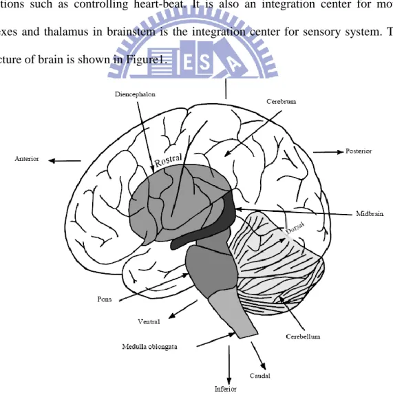
EEG is the potential change of brain. There are three blocks in a brain, including cerebrum, brainstem, and cerebellum. The function of cerebrum is associated with conscious and the functions of cerebellum are related to balance and voluntary muscle movements. There are some main functions of brainstem. The first one is primitive functions such as controlling heart-beat. It is also an integration center for motor reflexes and thalamus in brainstem is the integration center for sensory system. The structure of brain is shown in Figure1.
3
Cerebrum is divided into two blocks, gray matter and white matter. EEG signals are produced from neurons in gray matter and neurons are composed of synapses, dendrite and axon. Acetylcholine, glutamate, and dopamine, which form neurotransmitter, are released from synapses and opens the channel of ion and produces micro current out of a cell. Human cerebral cortex in gray matter contains a large amount of neurons and the micro current may produce potential changes. In the other words, potential changes are composed of the Electrical Rhythms and Transient Discharge.
EEG is a non-invasive tool for recording electrical activity by neurons within brain and it can measure locations, frequency ranges, amplitudes, and waveforms. EEG provides important information about the healthcare status of central nervous system (CNS) [7]. In medical application of neurology, it is common to use EEG to diagnose diseases such as tumor, epilepsy, encephalopathy and brain death.
For example, epilepsy is an abnormal activity of discharge from brain. When epilepsy occurs, a spike will appear and the spike should be monitored to reduce influence of epilepsy attacks. So it is necessary to know the normal EEG. A typical voltage range of EEG signal is about 10 μVolt to 100 μVolt, and the frequency domain is less than 50 Hz. In addition, there are four major bands of a continuous rhythmic sinusoidal EEG activity. They are recognized as δ (delta, below 4Hz), θ (theta, 4-8Hz), α (alpha, 8-12Hz), and β (beta, 12-30Hz), and their characteristics are listed in Table 1.1. (activities below or above these ranges are likely to be considered as artifactual noise, under standard clinical recording techniques)
4
Table 1.1 The characteristics of EEG activities Type Frequency
Range (Hz)
Amplitude Range (μV)
Description
Delta (δ) 0~4 50 Delta waves often occur in a deep sleep stage, such as stage 3 or stage 4, and are associated with certain encephalopathies and underlying lesions.
Theta (θ) 4~8 Below 20 Theta waves can be seen during hypnagogic states such as trances, hypnosis, deep day dreams, and light sleep and just before falling asleep. Alpha (α) 8~12 20~80 Alpha waves are produced from
occipital lobe, and are the characteristic of relaxed, alert state of consciousness. It disappears in deep sleeping.
Beta (β) 12~30 Below 20 Beta waves are produced from Frontal and parietal lobes. Beta waves are often associated with active, busy or anxious thinking and active concentration.
1.1.2 Electrocardiogram
In a heart muscle cell, electric activation takes place by means of the same mechanism as in a nerve cell. Electrocardiography (ECG) is an interpretation of electrical and muscle activities of heart over time captured and externally recorded by skin electrodes [8]. Electrodes can be used to detect tiny electrical changes on skin that are caused when heart muscle depolarizes and repolarizes for recording ECG. Two electrodes are combined into a number of pairs and the output from each pair is known as a lead. Different types of ECG measurements require different numbers of recorded leads such as 3-lead, 5 lead, and 12-lead ECGs. A 12-lead ECG is one in which 12 different electrical signals are recorded at approximately the same time and will often be used as a one-off recording of ECG, typically printed out as a paper copy.
5
3-lead and 5-lead ECGs tend to be monitored continuously and viewed only on the screen of an appropriate monitoring device, for example during an operation or whilst a patient is transported in an ambulance.
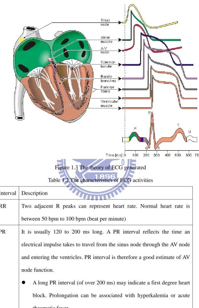
A normal ECG has P waves, QRS waves, and T waves as shown in Figure 1.2. A P wave is produced by atrial depolarize and a QRS wave is produced by ventricular depolarize. A T wave is produced by ventricular repolarize. Atrial repolarize is much smaller than a QRS wave and it can be ignored, because of the stronger ventricular muscle as shown in Figure 1.3. The three most commonly used intervals are listed in Table 1.2 along with their usages and descriptions.
6
Figure 1.3 The theory of ECG generated Table 1.2 The characteristics of ECG activities Interval Description
RR Two adjacent R peaks can represent heart rate. Normal heart rate is between 50 bpm to 100 bpm (beat per minute)
PR It is usually 120 to 200 ms long. A PR interval reflects the time an electrical impulse takes to travel from the sinus node through the AV node and entering the ventricles. PR interval is therefore a good estimate of AV node function.
A long PR interval (of over 200 ms) may indicate a first degree heart block. Prolongation can be associated with hyperkalemia or acute rheumatic fever.
7
A short PR interval may indicate a pre-excitation syndrome via an accessory pathway that leads to early activation of the ventriclesm such as seen in Wolff-Parkinson-White syndrome.
A variable PR interval may indicate other types of heart block.
QT A QT interval generally represents electrical depolarization and repolarization of the left and right ventricles. A prolonged QT interval is a risk factor for ventricular tachyarrhythmias and sudden death.
ECG is a noninvasive recording produced by an electrocardiographic device. The bandwidth is from 0 Hz to 150 Hz and the amplitude is about 100uV. Heart rate (HR) is a non-stationary value; It can vary as the body’s need to absorb oxygen and excrete carbon dioxide changes, such as during exercise or sleep. The measurement of heart rate is used by medical professionals to assist in diagnoses and tracking of medical conditions.
Heart rate variation (HRV) is measured as the variation in the beat-to-beat interval and it may contain indicators of current disease, or warnings about impending cardiac diseases. The difference in frequency ranges allows HRV analysis to distinguish sympathetic from parasympathetic contributions evidently [9].
The bandwidth of ECG is from 0 Hz to150 Hz and amplitude of ECG is about 100uV. Premature ventricular contraction (PVC) can be diagnosed by investigating ECG. There are some causes of arrhythmia such as anxiety, hypoxia, and caffeine. If patients’ situations get worse, there may be Ventricular Tachycardia (VT) or Ventricular Fibrillation (VF), and the worst case is possible death.
On the other hand, time-frequency parameters calculated using wavelet transform and extracted from the nocturnal heart period analysis appeared as powerful
8
tools for obstructive sleep apnoea syndrome diagnosis. Time-frequency domain analysis of the nocturnal HRV using wavelet decomposition could represent an efficient market of obstructive sleep apnoea syndrome [10].
1.1.3 Near-Infrared Spectrogram on Human Tissue
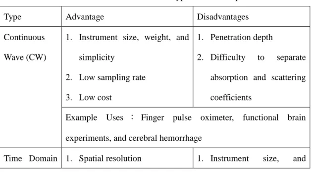
It is a kind of non-invasive and real-time radiography and can detect tumors in breast and brain. Diffuse Optical Tomography (DOT) technology has been widely used and studied in recent years. Using an array of near-infrared rays (NIR) source and detector pairs, a map of received light intensities can be established from which the DOT image can be calculated and displayed for medical analysis and diagnosis. DOT can be used to detect oxygenated hemoglobin (HbO) and deoxygenated hemoglobin (Hb) concentration. Therefore, the main application of DOT in clinical is to monitoring oxygen saturation and tumors within brain and breast. There are three types of measurement of the diffused near-infrared light, DOT can be divided into three main categories: the continuous wave (CW), frequency domain and time domain.
Table 1.3 Characteristics of the three main types of diffuse optical measurements Type Advantage Disadvantages
Continuous Wave (CW)
1. Instrument size, weight, and simplicity
2. Low sampling rate 3. Low cost
1. Penetration depth
2. Difficulty to separate absorption and scattering coefficients
Example Uses : Finger pulse oximeter, functional brain experiments, and cerebral hemorrhage
9
(TD) 2. Penetration depth
Most accurate separation of absorption and scattering coefficients
weight
2. High sampling rate 3. Stabilization and cooling Cost
Example Uses:Imaging cerebral oxygenation and breast imaging Frequency
Domain (FD)
1. Relative accurate separation of absorption and scattering coefficients
2. Relatively low sampling rate
1. Cost
2. Instrument size weight 3. Penetration DEPTH
Example Uses:Cerebral and muscle oximetry and breast imaging Table 1.3 shows the characteristics of different DOT systems. The advantages of the CW system include high portability, low cost, low power consumption and computation overhead [11]. On the other hand, the volume of the CW-DOT system can be miniaturized and this is the biggest advantage compared to other algorithms. Therefore, the CW-DOT system is the most feasible candidate for hardware implementation. However, little literature has been published on such implementation of CW-DOT signal processing. Most CW-DOT system post-process signals offline by computers [12-13]. This way, portability is out of question. Using the VLSI technology to implement to miniaturize the system will improve the development of DOT.
1.2 The Important Development of HealthCare System
System-on-a-chip (SOC) technology has made possible the practical development of many functionally-rich consumer electronic products, for instance, mobile TVs, cell phones, and so on. In recent years, biochip has emerged as another active topic in the field of SOC research, with many new exciting technologies such as DNA-chip,
10
Electroencephalograph (EEG) and Electrocardiogram (ECG) monitoring chip, etc. currently engaged in the development pipeline. With SOC technology, highly-integrated, low cost and portable biomedical devices can be realized, allowing medical diagnostics typically performed at the hospital to be conducted at the comfort and convenience of the patients’ homes.
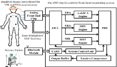
The realization of portable devices for EEG or ECG recording that allows unrestricted patient mobility is of great relevance to many biomedical applications. Figure 1.4 shows the portable real-time diagnostic system which can detect a user’s biomedical signals and transport the data back to a base station system for display and analysis by a doctor or medical technologist.
Figure 1.4 The architecture of portable real-time diagnostic system
The development of portable sensors is highly important in the health care system, particularly in instrumentation for medical diagnostics and detection systems. EEG and ECG signals are both considered to be useful signals for diagnostic system [14]. But all of them are weak signals, and are easily affected by various kinds of noise especially power-line noise. Furthermore, EEG and ECG signals have different amplitudes and bandwidths; therefore, it is necessary to design an adjustable gain factor and bandwidth system which can detect these signals concurrently.
AFE Channel x 7 CHDDA X100 IN1-1 IN1-2 IN1-3 Vbias CHDDA CLK Adjustable Gain Stage1 X1/X40 LPF Adjustable Bandwidth 50/150 Filter CLK CLK Notch Filter 60Hz Adjustable Gain Stage2 X1/X40 LPF Adjustable Bandwidth 50/150 Filter CLK Vout DOT x 1
Analog Front-End Chip
Brain-Heart Monitoring Chip
FICU 4-CH ICA 3-CH HRV Engine DOT Engine PDS EEG ECG NIR System Control Unit
UART Lossless Compressor Output Buffer Analog Multiplexer SAR-ADC -Lead I+ - Le ad II+ - L e a d II I+ EEG ECG DOT Bluetooth Module Smart Phone DOT Sensor 4-CH EEG HAT
11
1.3 The Solution of Highly Integrated Healthcare System
In order to develop a portable biosensor that can detect biomedical signals for medical diagnosis, the AFE IC is designed with two properties: low power and support for multiple channels. In this design, a fully integrated eight-channel AFE IC which with four channels for EEG, three channels for ECG and one channel for DOT is proposed. The output of the AFE IC is linked to the back-end for further digital signal processing. This includes ICA, HRV and DOT processing which helps doctors in making more accurate diagnoses.
1.4 Contribution of This Work
The development of portable brain-heart monitoring systems is not only useful in long-term healthcare, but also demanded in an increasing number of researches in the biomedical field [15]. This thesis presents a highly integrated analog front-end (AFE) IC design that helps to realize the idea of new miniaturized portable instruments for monitoring brain-heart biosignals, such as diffuse optical tomography (DOT) signals, electrocardiography (ECG) signals, and electroencephalography (EEG) signals.
An integrated portable system with the ability to wirelessly transmit data to a science station will have the follow advantage:
Much more comfort for subjects being observed
Lower chance of inaccurate measurement caused by discomfort Short writing for feeble physiological electrical signals
Lower cost
Extended applicable range of system
Biomedical signals are acquired from the proposed front-end IC and further processed by the brain-heart monitoring chip which comprises a DOT processor for brain imaging reconstruction, an independent component analysis (ICA) processor for
12
EEG signal analysis, and a heart rate variability (HRV) analysis processor for ECG signal analysis. The processed data or biomedical signals are then lossless- compressed and sent to a smart phone for real-time display or a science station for further analysis and 3D visualization [16].
1.5 Organization of the Thesis
The organization of this thesis is as follows. In Chapter 2, a low power and high integrated 8-channel analog front-end IC (AFE IC) is provided for home care system. The main amplifier has characteristic of low noise and low power is presented in section 2.2. The operation amplifier of low pass filter and amplifier is show in section 2.3. For a better area efficient IC, the adjustable gain amplifier and adjustable bandwidth low pass filter are presented in section 2.4 and 2.5. To avoid power line noise, the notch filter is shown in section 2.6. There are some problems about signal channel and time delay shown in section 2.7 and section 2.8. The clock generator for chopper differential difference amplifier and low pass filter is shown in section 2.9. Then, the 8-channel shares the same ADC by 8-to-1 multiplexer as shown in section 2.10. In section 2.11, it is talking about a successive approximation register analog-to-digital converter, and the ADC converters biomedical signals to digital signals for signal processing. Finally, the tape-out summary of the designed 8-channel AFEIC using TSMC 0.18UM CMOS Mixed Signal RF General Purpose Standard Process FSG AL 1P6M 1.8&3.3V process technology is presented in section 2.12.
Chapter 3 describes the measurement environment and test result. Finally, the conclusion and future work is given in chapter 4.
13
Chapter 2 8-Channel Analog Front-End IC
In this chapter, the design of an 8-channel analog front-end (AFE) IC for portable brain-heart monitoring applications is shown in Figure 2.1. The AFE IC is highly-integrated and employed to detect bio-medical signals such as electroencephalography (EEG) signals, electrocardiography (ECG) signals and diffuse optical tomography (DOT) signals. The developed IC features a fully integrated eight-channel design which includes one channel for DOT, three channels for ECG, and four channels for EEG. Each channel is composed of a chopper differential difference amplifier (CHDDA), a low-pass filter and an analog-to-digital converter (ADC) as shown in Figure 2.2. To consider about time delay for EEG signal processing, independent component analysis (ICA), the architecture of 8-channel AFE used the same seven channels in IC.
Figure 2.1 The architecture of 8-channel front-end IC
Figure 2.2 The architecture of one channel Four
channels for EEG
Three channels for ECG
14
In order to develop a portable biosensor that can detect signals and to let diseases can be diagnosed accurately. The front-end circuit requires two properties, one is low power and the other is multi-channels. In this design, there is an 8-channel analog front-end circuit which includes four channels for EEG, three channels for ECG and one channel for DOT. Then the front-end circuit is linked to back-end for signal processing as shown in Figure 2.3. The independent component analysis (ICA) engine, heart rate variability (HRV) engine and diffuse optical tomography (DOT) engine can help doctors to diagnose. Finally, biomedical signals are delivered to a science station and a clinic through a universal asynchronous receiver transmitter (UART) and Bluetooth.
The architecture of the system is shown in section 2.1. In order to achieve the goals of lower power, lower noise, and more efficient area utilization, in section 2.2, the circuit of amplifier and the reasons why the system chose this architecture are presented and described in detail. The circuit of the filter is then illustrated in section 2.3 and the circuit of ADC is shown in section 2.4, they are also illustrated in detail. Finally in section 2.5, the tape-out summary of the fabricated chip using TSMC 180nm CMOS technology is presented.
15
2.1 The Architecture of 8-channel Analog Front-End IC
The development of portable brain-heart monitoring systems is not only useful in long-term healthcare, but also demanded in an increasing number of researches in the biomedical field. A highly integrated AFE IC design is presented in this thesis and the AFE IC helps to realize the idea of new miniaturized portable instruments for monitoring brain-heart bio-medical signals, such as DOT signals, ECG signals, and EEG signals. Figure2.4 shows the system-on-chip (SoC) based hardware architecture of the wireless portable brain-heart monitoring system presented in study [16]. This system includes a set of multi-channel dry-electrodes [17], a proposed AFE chip, a brain-heart monitoring chip [16], a Bluetooth module, and a smart phone. Biomedical signals are acquired from the proposed front-end IC and further processed by the brain-heart monitoring chip which comprises a diffuse optical tomography (DOT) processor for brain imaging reconstruction, an independent component analysis (ICA) processor for EEG signal analysis, and a heart rate variability (HRV) analysis processor for ECG signal analysis. The processed data or biomedical signals are then lossless-compressed and sent to a smart phone for real-time display or a science station for further analysis and 3D visualization.
In order to achieve the low-power and low-noise AFE IC design goals, a new programmable readout channel is designed for all EEG and ECG channels. This readout channel is composed of a chopper-stabilized differential difference amplifier (CHDDA) [18], an adjustable gain amplifier, and an adjustable low pass filter (LPF). A 10-bit successive approximation register analog-to-digital converter (SAR-ADC) is also employed in conjunction with an analog multiplexer to select a particular bio-medical signal for analog-to-digital conversion. Since the signals are vulnerable, they are easily influenced by various kinds of noise. A modified CHDDA is designed
16
for rejecting differential electrode offset and common mode disturbance. It solves the DC offset problem of past designs [18-19] by adding an independent and stable DC offset circuit. Furthermore, an adjustable gain amplifier and adjustable bandwidth low pass filter are also designed for adjusting the gain and bandwidth for different signals. This modified LPF design replaces the resistors by switch-capacitor technology to increase the area efficiency [20-21]. The L.P.F. design also achieves the low power feature by adopting the Sallen-Key scheme [22] which is based on a single amplifier at low power. Finally, the SAR-ADC is designed for applying in bio-medical with the feature of low power and high accuracy.
Figure 2.4 Portable brain-heart monitoring system overview
2.2 Chopper Differential Difference Amplifier
There are a lot of researches related to instrumentation amplifier (IA), some had three-op-amp instrumentation amplifiers [23], the other had used current amplifiers [24], and in this design, the chopper differential difference amplifier (CHDDA) [18-19] is used to amplify biomedical signals.
17
accurate signals, the first stage is to use a CHDDA to amplify biomedical signals. In the past, the common approach is to use a three-op-amp IA. However, it not only requires larger area and consumes much more power, but also is prone to reduce common mode rejection ratio (CMRR) by fabrication mismatch. In other way, although the area of current feedback amplifier is not large, the power of it is a little too much in biomedical field. The most important reason is biomedical signals are longtime-observed weak signals, so chopper technology is used to amplify the biomedical signals with low power consumption.
There are some features of chopper such as low noise, low power, high tolerance…etc. But the most important feature is its’ low noise, the chopper circuit converts low frequency noise into high frequency one. Then the high frequency noise can be removed by a low pass filter (L.P.F.) and the biomedical signals can be converted back to their original frequency. Biomedical signals are only changed in form, from continuous-time signals to discrete-time signals, and the sample frequency is much higher than frequency of biomedical signals, so the biomedical signals are like almost the same as they were. Moreover, biomedical signals don’t change frequently, so the chopper circuit has no influence on real biomedical signals, the data that doctors need to make judgments.
The CMRR of general IAs is affected easily by the mismatch of resistors, capacitors and transistors. In addition, the influence at issue is serious. The differential difference amplifier (DDA) which is shown in Figure 2.5 can modify this defect, because CMRR is only related to the mismatch of the input ports. A DDA just requires a single active amplifier and two capacitors to set the gain, so the influence of the mismatch issue on the gain is little.
18
difference pair technology. Vnn and Vnp are connected to input biomedical signals, Vpp is connected reference voltage and Vpn is connected to the feedback circuit. Inputs are connected to chopper circuits, what they display is as the boxes in Figure 2.5, to convert low frequency noise to high frequency noise. The M1~M4 are input pairs and M5 and M6 supply current for the circuit. Then M1~M4 convert signals from voltage type to current type, M7 and M8 convert signals back to voltage type and convey them to M9~M14 to be amplified. Finally, the boxes are the chopper circuits as shown in Figure 2.6. It is necessary to provide two non-overlapping clocks for chopper circuits, the clocks will be discussed in section 2.8. The feature of chopper circuit is to cover a normal signal to a high frequency and discontinue signal. In the biomedical domain, physiological signals show no large diversification, so discontinue signals may not affect final result. And the most important is another feature, converting a normal signal to a high frequency signal. This way, low frequency noise such offset noise can be converted to high frequency noise and removed by a low pass filter which will be discussed in section 2.5.
19
Figure 2.6 The circuit of chopper technology
Figure 2.7(a) The feedback architecture of CHDDA (b) Using Capacitor feedback to replace the resistor feedback
Biomedical signals are weak signals, so it is necessary to amplify them until reaching an appropriate level. For signal processing in the back-end, the gain of CHDDA is 40dB and the circuit is shown in Figure 2.7 (a). In Figure 2.7 (a), the gain is decided by the resistors, R1 and R2, and Equation 2.1 shows the gain. The characteristic of this design is system on chip, so all components are on a chip include resistors. Just like the above mentioned, it is necessary to control the power consumption for long time observation. The current must be low enough to control the power consumption. This way, the resistors may become too large, making it difficult to implement on the chip. To solve the problem, the design replaces resistors by capacitors as shown in Figure 2.7 (b). The Equation 2.2 can be used to determine the
20
gain. Finally, the sizes of all transistors are listed in Table 2.1.
2.1 2.2 Table 2.1 The sizes of transistors
Devices W/L (um) M1~M4 5/0.9 M5~M6 5/0.9 M7~M10 1.4/0.9 M11~M12 5/0.9 M13~M14 5/0.6
The chopper differential difference amplifier (CHDDA) which is DDA using the chopper technology also has some features such as high tolerance to mismatch of input ports, high CMRR, and low input offset noise. And the CHDDA uses only one active amplifier, so the area is smaller than a 3OPIA which uses three active amplifiers.
When applying it in the biomedical field, it is usually set on patients’ bodies. It is not only inconvenient but also uncomfortable for patients. As for the portable AFE IC, it is necessary to think about the convenience of patients. The movement of patients may lead to a large DC offset so that the AFE circuits may enter the saturation region.
In order to solve this problem, the design makes an impendent reference [25] voltage for CHDDA. This impendent reference voltage is composed of capacitors as show in Figure 2.8. First, capacitors are used at the input of the CHDDA to avoid any DC offset and then giving inputs some transistors and another reference voltage. This way, it creates a new independent DC offset to input by diode-connected MOS which
21
controls the level of DC offset to keep the circuit work normally.
Figure 2.8 The control circuit of impendent reference voltage
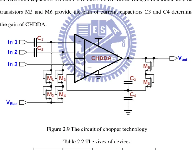
The modified CHDDA with an independent and stable DC offset circuit is shown in Figure 2.9. The transistors M1~M4 provide new impendent reference voltage to CHDDA and capacitors C1 and C2 remove the DC offset voltage. In another way, the transistors M5 and M6 provide the path of current, capacitors C3 and C4 determine the gain of CHDDA.
+ - CHDDA + - + - In 1 In 2 In 3 VBias C1 C2 C3 C4 M1 M2 M3 M4 M5 M6 Vout
Figure 2.9 The circuit of chopper technology Table 2.2 The sizes of devices
Devices Value Devices W/L (um) C1~C2 5 p M1~M4 1/1
C3 0.1p M5~M6 1/1 C4 10p
22
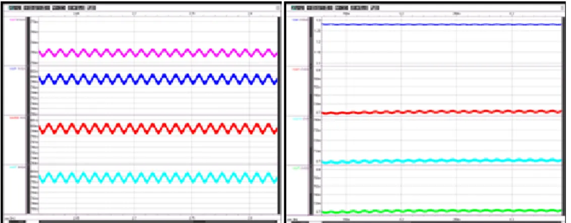
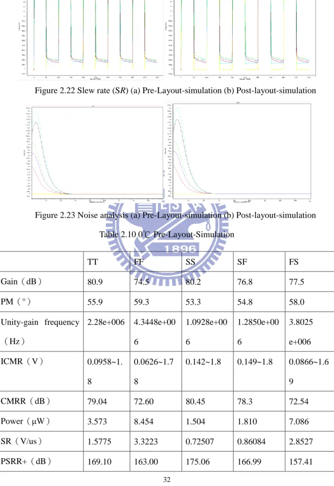
The simulation results are shown below in Figure 2.10, Figure 2.11, Figure 2.12, Figure 2.13, and Figure 2.14. The yellow line represents the input signal, black line represents the TT process; red line represents the FF process; blue line represents the SS process; green line represents the SF process; purple line represents the FS process.
Figure 2.10 Frequency response (a) Pre-Layout-simulation (b) Post-layout-simulation
Figure 2.11 Common-mode rejection ratio (CMRR) (a) Pre-Layout-simulation (b) Post-layout-simulation
23
Figure 2.12 Input common-mode range (ICMR) (a) Pre-Layout-simulation (b) Post-layout-simulation
Figure 2.13 Slew rate (SR) (a) Pre-Layout-simulation (b) Post-layout-simulation
24
Figure 2.15 Function simulation of CHDDA (a) Pre-Layout-simulation (b) Post-layout-simulation:
Figure 2.16 Function simulation of modified CHDDA
25
In Figure 2.15(a), the blue line is input signal and the pink is output signal, and the green line is input and blue line is output in the Figure 2.15 (b). The Figure 2.16 show the independent reference voltage simulation, the blue line is input signal and the red line is output. In Figure 2.16, the output will follow the DC level independent reference voltage and amplify the input normally as show in Figure 2.17. In this way, the design will transform the signal from low frequency to high frequency without distortion.
The parameter simulations of DDA are shown in Table 2.3, Table 2.4, Table 2.5, Table 2.6, Table 2.7, and Table 2.8.
Table 2.3 0℃ Pre-Layout-Simulation TT FF SS SF FS Gain(dB) 73.1 66.5 73.5 70.2 69.1 PM(°) 95.9 79.4 111.9 38.9 74.3 Unity-gain frequency (Hz)
3.7778E+05 4.8505E+05 7.8542E+05 8.6699E+06 4.1905E+05
ICMR(V) 0.591~1.02 0.593~1.02 0.58~1.03 0.502~1.1 0.635~0.968 CMRR(dB) 75.7 69.75 76.4 76.36 59.6 Power(μW) 20.9 32.6 27.3 23.3 27.8 SR(V/us) 0.9642 1.8227 0.4649 5.3408 0.5430 PSRR+(dB) 115.21 100.08 119.14 115.97 101.40 PSRR-(dB) 103.21 91.911 105.71 101.05 95.362 total equivalent 0.621 1.3 0.243 1.07 0.317
26 Table 2.4 25℃Pre-Layout-Simulation Table 2.5 80℃ Pre-Layout-Simulation noise (nV) Output range 0.0117~1.09 0.016~1.09 0.009~1.08 0.038~1.15 0.0043~1.06 TT FF SS SF FS Gain(dB) 73.2 66.3 73.8 70.5 68.8 PM(°) 91.9 75.3 119.1 30.0 73.9 Unity-gain frequency (Hz)
3.5643E+05 5.8187E+05 5.7070E+05 9.4152E+06 4.5284E+05
ICMR(V) 0.602~1.01 0.621~0.983 0.613~0.99 0.112~1.06 0.674~0.944 CMRR(dB) 75.88 70.37 76.71 76.27 61.08 Power(μW) 22.0 41.5 20.3 25.6 34 SR(V/us) 0.7795 1.7367 0.5407 5.8539 0.7193 PSRR+(dB) 112.66 99.256 118.61 115.56 102.03 PSRR-(dB) 102.82 91.636 105.47 100.40 95.338 total equivalent noise (nV) 0.871 1.63 0.396 1.35 0.5 Output range 0.0117~1.09 0.016~1.09 0.009~1.08 0.038~1.15 0.0043~1.06 TT FF SS SF FS Gain(dB) 72.8 65.7 74.0 70.5 68.3 PM(°) 77.9 69.7 100.4 51.1 77.5
27 Table 2.6 0℃ Post-Layout-Simulation TT FF SS SF FS Gain(dB) 71.9 64.9 73.1 70.0 67.1 PM(°) 75.3 70.0 91.3 53.0 79.6 Unity-gain frequency (Hz) 5.3901E+ 05 8.3518E+ 05 3.2110E+0 5 1.0004E+ 07 3.6394E+ 05 ICMR(V) 0.7~1.11 0.73~1.08 0.717~1.0 9 0.659~1.1 5 0.755~1.0 6 CMRR(dB) 75.70 69.77 76.40 76.36 59.61 Power(μW) 21.58 40.37 12.31 19.72 29.46 SR(V/us) 1.1248 2.1177 0.47302 5.1650 0.56527 PSRR+ 115.95 100.69 119.61 116.35 101.41 PSRR- 103.23 91.94 105.72 101.07 95.383 frequency (Hz) ICMR(V) 0.587~1.03 0.606~0.992 0.602~1 0.22~1.1 0.641~0.956 CMRR(dB) 76.17 71.83 77.07 75.89 64.04 Power(μW) 36.4 61.5 21.0 36.6 42.1 SR(V/us) 3.0382 4.8994 1.6505 5.1185 1.5855 PSRR+(dB) 109.00 99.180 115.84 114.24 102.92 PSRR-(dB) 101.82 90.942 104.73 99.026 95.045 total equivalent noise(nV) 1.43 2.28 0.805 1.94 0.967 Output range 0.0144~1.11 0.019~1.11 0.018~1.10 0.040~1.16 0.0058~1.07
28 total equivalent noise(nV) 0.565 1.18 0.021 0.963 0.288 Output range 0.0162~1. 12 0.0201~1. 12 0.0135~1. 11 0.0341~1. 16 0.0825~1. 08 Table 2.7 25℃ Post-Layout-Simulation TT FF SS SF FS Gain(dB) 71.6 64.6 72.9 69.7 67.0 PM(°) 72.1 68.2 82.8 98.6 77.5 Unity-gain frequency (Hz) 6.3231E+ 05 9.2234E+ 05 3.9871E+05 5.4272E+ 06 4.5152E+ 05 ICMR(V) 0.696~1.1 1 0.698~1.1 0.706~1.1 0.643~1.1 5 0.737~1.0 6 CMRR(dB) 75.88 70.39 76.71 76.28 61.09 Power(μW) 24.78 44.626 14.40 23.70 31.83 SR(V/us) 1.5845 2.9583 0.76405 3.5866 1.0072 PSRR+(dB) 113.41 99.28 119.11 115.91 102.04 PSRR-(dB) 102.84 91.67 105.48 100.42 95.36 total equivalent noise(nV) 0.789 1.47 0.359 1.22 0.451 Output range 0.0195~1. 14 0.0237~1. 14 0.0167~1.1 3 0.384~1.1 8 0.0106~1. 10 Table 2.8 80℃ Post-Layout-Simulation TT FF SS SF FS Gain(dB) 70.7 63.9 72.4 68.9 66.4 PM(°) 67.2 64.8 73.3 97.0 73.2
29 Unity-gain frequency (Hz) 8.1061E+ 05 1.0833E+ 06 5.6820E+ 05 1.0943E+ 06 6.2863E+05 ICMR(V) 0.6564~1. 14 0.676~1.1 2 0.669~1.1 3 0.621~1.1 9 0.726~1.1 CMRR(dB) 76.17 71.84 77.07 75.90 64.06 Power(μW) 38.48 63.81 23.53 37.50 46.04 SR(V/us) 2.9429 4.7379 1.6892 5.1871 1.6202 PSRR+ 109.02 99.20 116.48 114.57 102.94 PSRR- 101.84 90.97 104.74 99.0 95.07 total equivalent noise(nV) 1.39 2.09 0.738 1.78 0.884 Output range 0.0281~1. 19 0.033~1.1 8 0.0247~1. 17 0.05~1.22 0.0169~1.1 4
2.3 Operation Amplifier
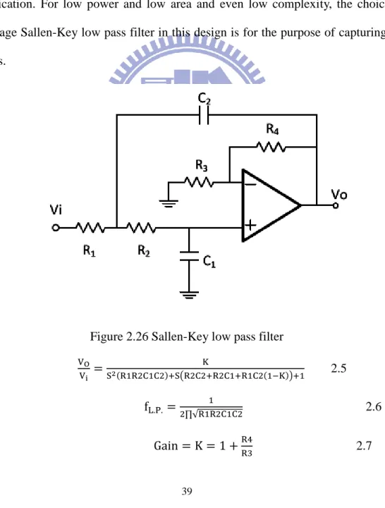
In this design, it is necessary to design an operation amplifier for low pass filter and adjustable gain amplifier. Because biomedical signals are weak signals, the operation amplifier must be of low noise. In another way, the physiological signals have to be observed for a long time to ensure the diagnoses of diseases are correct. For long time observation, the power consumption must be low enough to maintain system’s normal operation. The operation amplifier of is low noise and low power in this design as shown in Figure 2.18, Figure 2.19, Figure 2.20, Figure 2.21, Figure 2.22, and Figure 2.23.
30
Figure 2.18 The circuit of operation amplifier Table 2.9 The size of operation amplifier
Devices W/L (um) M1~M2 0.5/1 M3~M4 0.6/1 M5 1.2/1 M6 6/0.5 M7 1.2/0.5 Devices Value C1 0.5 p
The parameter simulations of OPA are shown in Table 2.10, Table 2.11, Table 2.12, Table 2.13, Table 2.14, and Table 2.15.
31
Figure 2.19 Frequency response (a) Pre-Layout-simulation (b) Post-layout-simulation
Figure 2.20 Common-mode rejection ratio (CMRR) (a) Pre-Layout-simulation (b) Post-layout-simulation
Figure 2.21 Input common-mode range (ICMR) (a) Pre-Layout-simulation (b) Post-layout-simulation
32
Figure 2.22 Slew rate (SR) (a) Pre-Layout-simulation (b) Post-layout-simulation
Figure 2.23 Noise analysis (a) Pre-Layout-simulation (b) Post-layout-simulation Table 2.10 0℃ Pre-Layout-Simulation TT FF SS SF FS Gain(dB) 80.9 74.5 80.2 76.8 77.5 PM(°) 55.9 59.3 53.3 54.8 58.0 Unity-gain frequency (Hz) 2.28e+006 4.3448e+00 6 1.0928e+00 6 1.2850e+00 6 3.8025 e+006 ICMR(V) 0.0958~1. 8 0.0626~1.7 8 0.142~1.8 0.149~1.8 0.0866~1.6 9 CMRR(dB) 79.04 72.60 80.45 78.3 72.54 Power(μW) 3.573 8.454 1.504 1.810 7.086 SR(V/us) 1.5775 3.3223 0.72507 0.86084 2.8527 PSRR+(dB) 169.10 163.00 175.06 166.99 157.41
33 Table 2.11 25℃ Pre-Layout-Simulation Table 2.12 80℃ Pre-Layout-Simulation PSRR-(dB) 128.94 114.62 135.60 130.75 118.81 total equivalent noise(nV) 3.4 10.1 0.96 1.27 8 Output range 0~1.79 0~1.78 0~1.8 0~1.8 0~1.78 TT FF SS SF FS Gain(dB) 80.8 74.0 80.7 77.1 77.15 PM(°) 56.1 59.5 53.4 54.9 58.0 Unity-gain frequency (Hz) 2.7895e+00 6 4.8849e+00 6 1.4525e+ 006 1.6809e+00 6 4.34 e+006 ICMR(V) 0.0515~1.8 0~1.8 0.0847~1 .8 0.0866~1.8 0~1.66 CMRR(dB) 76.13 69.67 79.16 77.9 69.5 Power(μW) 4.84 10.61 2.176 2.586 9.025 SR(V/us) 2.1298 4.1451 1.049 1.2252 3.6291 PSRR+(dB) 163.26 153.98 168.56 175.61 151.98 PSRR-(dB) 125.91 112.10 131.66 126.48 116.51 total equivalent noise(nV) 5.45 13.8 1.78 2.3 11.3 Output range 0~1.79 0~1.79 0~1.8 0~1.8 0~1.78 TT FF SS SF FS Gain(dB) 79.6 71.9 80.7 76.3 75.7 PM(°) 57.3 60.6 54.4 56.0 58.9
34 Table 2.13 0℃ Post-Layout-Simulation TT FF SS SF FS Gain(dB) 80.91 74.57 80.25 76.79 77.50 PM(°) 54.66 58.08 51.99 53.55 56.68 Unity-gain frequency (Hz)
2.2580E+06 4.3062E+06 1.0812E+06 1.2722E+06 3.7675E+06
ICMR(V) 0.076~1.79 0.0279~1.79 0.0856~1.8 0.0767~1.8 0~1.75 CMRR(dB) 79.04 72.6 80.45 78.32 72.54 Power(μW) 3.57 8.45 1.50 1.81 7.08 SR(V/us) 1.5742 3.3208 0.72393 0.85885 2.8516 PSRR+(dB) 169.10 163.01 175.06 166.99 157.41 PSRR-(dB) 128.90 114.58 135.57 130.71 118.77 Unity-gain frequency (Hz) 3.6615e+00 6 5.6238e+00 6 2.1976e+00 6 2.4687e+00 6 5.1361 e+006 ICMR(V) 0~1.78 0~1.62 0~1.79 0.07~1.8 0~1.54 CMRR(dB) 69.94 63.63 73.97 73.93 63.47 Power(μW) 7.90 15.21 4.011 4.656 13.26 SR(V/us) 3.4393 5.7679 1.8984 2.1777 5.2267 PSRR+(dB) 153.51 142.16 159.26 163.04 142.48 PSRR-(dB) 119.73 106.09 125.44 119.39 111.47 total equivalent noise(nV) 10.7 21 4.55 5.58 18.1 Output range 0~1.79 0~1.78 0~1.79 0~1.79 0~1.78
35 total equivalent noise(nV) 3.37 9.96 0.95 1.26 7.92 Output range 0~1.79 0~1.79 0~1.8 0~1.8 0~1.78 Table 2.14 25℃ Post-Layout-Simulation TT FF SS SF FS Gain(dB) 80.86 74.03 80.74 77.06 77.15 PM(°) 54.8 58.2 52.0 53.6 56.7 Unity-gain frequency (Hz)
2.7656E+06 4.8473E+06 1.4387E+06 1.6659E+06 4.3112E+06
ICMR(V) 0.0276~1.79 0.043~1.78 0~1.8 0~1.8 0~1.74 CMRR(dB) 76.14 69.67 79.16 77.9 69.54 Power(μW) 4.84 10.59 2.17 2.58 9.01 SR(V/us) 2.1283 4.1485 1.0423 1.2230 3.6305 PSRR+(dB) 163.26 153.99 168.56 175.62 151.98 PSRR-(dB) 125.87 112.07 131.63 126.45 116.48 total equivalent noise(nV) 5.41 13.7 1.77 2.28 11.2 Output range 0~1.79 0~1.78 0~1.8 0~1.8 0~1.78 Table 2.15 80℃ Post-Layout-Simulation TT FF SS SF FS Gain(dB) 79.57 71.86 80.67 76.35 75.71 PM(°) 55.95 59.31 53.03 54.71 57.55
36
Unity-gain frequency (Hz)
3.6406E+06 5.5967E+06 2.1829E+06 2.4536E+06 5.1086E+06
ICMR(V) 0~1.78 0~1.73 0~1.79 0~1.79 0~1.62 CMRR(dB) 69.94 63.63 73.97 73.93 63.47 Power(μW) 7.90 15.19 4.01 4.65 13.25 SR(V/us) 3.4508 5.8302 1.9027 2.1827 5.2541 PSRR+(dB) 153.51 142.17 159.26 163.04 142.49 PSRR-(dB) 119.70 106.07 125.41 119.37 111.44 total equivalent noise(nV) 10.7 21 4.54 5.57 18 Output range 0~1.79 0~1.78 0~1.79 0~1.79 0~1.78
2.4 Adjustable Gain Amplifier
Biomedical signals are weak and easily affected by external noise, so it is necessary to amplify them under low noise. In another way, different biomedical signals are of different amplitudes, for example, the range of EEG is usually represented in microvolt, while that of ECG is millivolt. To detect biomedical signals by using the same circuit for more efficient area utilization, the capability of adjustable gain is required.
Base on the above, the essential features of the amplifier are low noise and adjustability. Because the gain is always determined by resistors or capacitors, there are two methods to change the gain. One way is adding external resistors and according to gains adjusting the resistance of variable of resistors. Another way is
37
using control circuit to adjust the resistance or capacitance. First, it is necessary to determine the scale of gains and design some resistors or capacitors for the gain. Some resistors or capacitors can determine a lot of gains which can be adjusted by changing the value of resistors or capacitors.
For the convenience of patients, it is necessary to design a highly integrated AFE IC. This way, the amplifier would have adjustable gains on the IC. The EEG signals and ECG signals are different biomedical signals, so the gains they need are different. The gain of EEG signals is 80dB and that of ECG signals is 40 dB. For the highly integrated AFE IC, the control circuit of the design is in the IC. To complete the adjustable gain in the IC, two problems are to be considered, area and power. The power consumption has to be low enough for portable applications, so the corresponding current is much small. If resistors are used to determine the gain, the resistors are too large to be implemented in the IC. Therefore, t the capacitors are used in the design to decide the gain. For the purpose of adjusting gain, a set of complementary switches are employed to control the gain factor [19-20] as shown in Figure 2.24.
In Figure 2.24, in order to set the gain to 40, C1 and C3 are set to 1p and C2 to 0.05p. When S1 is closed, the gain is calculated using Equation 2.3. When S1 is opened, the gain is calculated using Equation 2.4 and is 1 approximately. This way, the amplifier becomes a buffer and also can reduce the interference between circuits. In this design, the amplifier is used to avoid amplifying noise in two stages and biomedical signals remain positive phase. The architecture of front-end circuit also includes a low pass filter connected to the amplifier to reduce the interference of noise. Figure 2.25(a), (b) show the simulation of adjustable gain amplifier, (a) is pre-simulation and (b) is post-simulation. The Figure 2.25(b) changes not only the
38
reference voltage but also gain of amplifier.
2.3 2.4
+
-
OP
V
REFV
inV
outC
1C
3C
2S
1S
1Figure 2.24 Adjustable gain amplifier
Figure 2.25 Simulation of adjustable gain amplifier (a) Pre-simulation (b) Post-simulation
2.5 Adjustable Bandwidth Low Pass Filter
Different biomedical signals have not only different amplitudes, but also different bandwidths. The bandwidth of EEG is from 0.01 Hz to 50 Hz while that of ECG is from 0.1 Hz to 150 Hz. Therefore, an adjustable bandwidth LPF is used to acquire the two different signals. Moreover, just like the adjustable gain amplifier, it has the feature of low area and low power. For portable applications, a two-stage Sallen-Key
39
low pass filter (L.P.F.) is used for its low power feature. The architecture of the Sallen-Key LPF shown in Figure 2.26 requires only one single amplifier, so that the power consumption of the filter is less than that of past designs [22]and the mismatch effect is not too significant. Equation 2.5 shows the frequency of the Sallen-Key low pass filter, and the cut-off frequency is determined by R1, R2, C1, and C2 as shown in Equation 2.6. Finally, the gain of the two stage Sallen-Key low pass filter is shown in Equation 2.7. The reason why using two stages is that the decreasing slope of two-stage L.P.F. is higher than one stage and the slope is also high enough to conform specification. For low power and low area and even low complexity, the choice of two-stage Sallen-Key low pass filter in this design is for the purpose of capturing the signals.
Figure 2.26 Sallen-Key low pass filter
2.5
2.6
40
As for another problem, because the power consumption is low and it makes the current low, too. This way, the resistors in the Sallen-Key LPF will be too large to be implemented on the chip. The design replaced the resistors with switch-capacitor technology [26-27] as shown in Figure 2.27, with one capacitor and two switches. And Equation 2.8 shows the capacitors replace the resistors.
Figure 2.27 The architecture of Switch capacitor technology
2.8
+
-
OP
V
outV
inC
SW1C
2C
SW2C
1C
3Ψ
1Ψ
2Ψ
2Ψ
2Ψ
2Ψ
1Figure 2.28 Switch-capacitor low pass filter
Because biomedical signals have different bandwidths, the L.P.F. circuit similarly employs a set of complementary switches to control the scale of capacitors to adjust bandwidth. The original cut-off frequency is obtained by Equation 2.6. If Ψ1 is closed, the cut-off frequency can be obtained by Equation 2.9. Otherwise, Equation 2.10 is used when the cut-off frequency of Ψ1 is opened. Finally, Figure 2.28 shows the modified switch-capacitor low pass filter. The pre-simulation and post-simulation of
41
EEG L.P.F. are show in Figure 2.29 (a) (b), and the simulations of ECG L.P.F. are show in Figure 2.29 (a) (b). The bandwidth of EEG is 50Hz and ECG is 150Hz, the output amplitude of signals are reduced to half of input signals, but the bandwidth of post-simulation is a little larger than pre-simulation for the stray capacitance.
2.9
2.10
Figure 2.29 Simulation of EEG low pass filter (a) Pre-simulation (b) Post-simulation
Figure 2.30 Simulation of ECG low pass filter (a) Pre-simulation (b) Post-simulation
2.6 Notch Filter
In practical applications, there are two sources of 60 Hz power-line noise, the noise may come from human body contact or is sensed through the electrodes and the power-line. The noise is often much stronger than the desired biomedical signals. To
42
obtain highly accurate signals, a notch filter is used to reduce this 60 Hz power-line noise. Then, with notch filter, employment of operation amplifiers is avoided in order to achieve the goal of low power and small area as shown in Figure 2.31. This way, the notch filter without any operation amplifier consumes less power than others. Although the decreasing slop is not as good as the one with an operation amplifier, the slop is high enough to reduce the power-line noise. But there is another problem, the power consumption will be low enough to be taken care for long time and the current will be low. In this circuit, the resistors can be implemented using PMOS as a substitute as shown in Figure 2.32. Finally, the modified notch filter is show in Figure 2.33. The pre-simulation and post-simulation are show in Figure 2.34(a), (b), the cut-off frequency in pre-simulation is 63.3Hz and 61.4Hz in post-simulation.
Figure 2.31 Notch filter