國
立
交
通
大
學
電機學院微電子奈米科技產業研發碩士班
碩
士
論
文
非對稱性 LDD 金氧半元件之單刀雙擲開關應用於
超寬頻 3.1~10.6GHz 之研究
Asymmetric-LDD MOS of SPDT Switch for
Ultra Wideband 3.1~10.6GHz
研 究 生:李佩諭
指導教授:荊鳳德 教授
鄭裕庭 教授
非對稱性 LDD 金氧半元件之單刀雙擲開關
應用於超寬頻 3.1~10.6GHz 之研究
Asymmetric-LDD MOS of SPDT Switch
for Ultra Wideband 3.1~10.6GHz
研 究 生:李佩諭 Student:Pei-Yu Lee
指導教授:荊鳳德 博士 Advisor:Dr. Albert Chin
鄭裕庭 博士
Dr.
Yu-Ting
Cheng
國 立 交 通 大 學
電機學院微電子奈米科技產業研發碩士班
碩 士 論 文
A Thesis
Submitted to College of Electrical and Computer Engineering National Chiao Tung University
in partial Fulfillment of the Requirements for the Degree of
Master in
Industrial Technology R & D Master Program on Microelectronics and Nano Sciences
January 2008
Hsinchu, Taiwan, Republic of China
i
非對稱性 LDD 金氧半元件之單刀雙擲開關
應用於超寬頻 3.1~10.6GHz 之研究
學生:李佩諭
指導教授:荊鳳德 博士
鄭裕庭 博士
國立交通大學電機學院產業研發碩士班
摘
要
本論文研究採用 0.18 微米互補式金氧半製程之應用於超寬頻 3.1-10.6GHz 的發射接收開關,採用串並的架構。電路中使用較高的汲極崩潰電壓之非對稱式 的 LDD 金氧半電晶體,故可加較大的偏壓以改善功率線性度;除此之外也使用基 極 浮 接 的 方 式 來 改 善 收 發 開 關 之 線 性 度 及 功 率 承 載 能 力 。 晶 片 的 大 小 為 0.325mm2,有效面積為 0.11mm2。量測結果最大植入損耗發射端與接收端分別 為 1.8dB 和 4.1dB,功率承載能力則達 28.7dBm。針對接收狀態下植入損耗過大 之缺點修改設計,根據模擬結果最大植入損耗發射端與接收端分別為 0.94dB 和 1.29dB,除此之外,功率承載能力可增至 30.1dBm,電路佈局面積為 0.21mm2, 有效面積為 0.055mm2。
ii
Asymmetric-LDD MOS of SPDT Switch
for Ultra Wideband 3.1~10.6GHz
Student:Pei-Yu Lee
Advisors : Dr.
Albert Chin
Dr. Yu-Ting Cheng
Industrial Technology R & D Master Program of
Electrical and Computer Engineering College
National Chiao Tung University
ABSTRACT
The topic of research is T/R switch for ultra-wideband 3.1-10.6GHz application, it was designed by series-shunt topology. The circuit is fabricated in 0.18µm CMOS process. The higher drain breakdown voltage of asymmetric-LDD MOS transistor is used for the transmitter path. The key point is the larger bias on the transmitter path to improve the power linearity. Besides, the body-floating technique is also used to improve the linearity and power-handling capability of T/R switch. The chip size is 0.325mm2. The effective area is 0.11mm2. The measured maximum insertion loss is 1.8dB and 4.1dB for transmitter and receiver respectively. The P1dB compression point is 28.7dBm. However, the higher insertion
loss is on the RX mode. Therefore the circuit has been redesigned in order to decrease the loss. According to the simulated result, the maximum insertion loss is 0.94dB and 1.29dB for transmitter and receiver respectively. Besides, the P1dB compression point can achieve 30.1dBm. The layout area is 0.21mm2. The effective area is only 0.055mm2.
iii
誌謝
本論文得以完成,首先要感謝我的指導老師 荊鳳德 教授以及
鄭裕庭 教授,在兩年的碩士研究生涯裡,給予我豐富的指導與照
顧,不論是研究上與生活裡都讓我在這兩年裡獲得許多的收穫。
另外我要感謝口試委員巫勇賢老師以及高瑄苓老師提出的指正及
建議,讓此篇論文更加完善。
我還要感謝張慈學長、金明鑄學長、張國慶學長、王鴻偉學長、
陳科閩學長、邱子倫學長、陳懿範學姐與翁正彥學長,他們在研
究上與學業上給我的幫助,讓我得以順利完成碩士研究。也要感
謝俊賢、建弦、群懿、膺任、富國以及實驗室大家,因為有你們
的陪伴與支持,讓我度過愉快又充實的兩年。
最後,我要對我的父母獻上最高的敬意與謝意,感謝父母對我
的栽培、支持與鼓勵,以及男友君達的陪伴,是我最大的精神支
柱才讓我有機會能接觸這一切並且完成我的學業與研究。
iv
Contents
Abstract (in Chinese)
……….………iAbstract (in English)
……….……….………...ii誌謝
…………...……….……….………iiiContents
……….……….……….ivList of Tables
………...………..………...viFigure Captions
………..…...………...viiChapter 1 Introduction
1.1 UWB……….……….….1
1.2 Motivation……….………2
Chapter 2 Basic Concept in Switch Design
2.1 Effects of Nonlinearity
2.1.1 Intermodulation...52.1.2 The 1-dB Compression Point and Third-Order Intercept Point………….…………9
2.2 Impedance Matching………..………..13
Chapter 3 How to Design Basic Switch
3.1 Introduction……….…………20
3.2 Basic Concept……….……21
3.3 Body-Floating Technique ...………...…………..………….……..26
v
Chapter 4 SPDT Ciurcuit1 Design
4.1 Circuit1 Topology……….………….……….………..…….…...33
4.2 Simulation and Measurement Result……….……….…..38
4.2.1 TX Mode………...……….38
4.2.2 RX Mode……….………….42
4.3 Summary………..……….…….…..46
Chapter 5 SPDT Circuit2 Design
5.1 Circuit2 Topology………..……….…..…….…...47
5.2 Simulation Result………...……….…..49
5.3 Summary………..……….……….…..55
Chapter 6 Conclusion
………….………...….………...56References
……….……….57Vita
……….………60vi
List of Tables
Chapter 4 SPDT Circuit1 Design
Table 4.1 The state of transistor on the circuit………..………35 Table 4.2 Comparison of T/R switch performance………..……….46
Chapter 5 SPDT Circuit2 Design
Table 5.1 The state of transistor on the circuit2….………...48 Table 5.2 The specification of circuit2……….54 Table 5.3 The comparison of T/R switch performance………55
vii
Figure Captions
Chapter 1 Introduction
Figure 1.1 Time-division duplexing………...4
Figure 1.2 A typical RF-front end block diagram………..4
Chapter 2 Basic Concept in Switch Design
Figure 2.1 Definition of the 1-dB compression point………6Figure 2.2 Corruption of a signal due to intermodulation between two interferes……8
Figure 2.3 The third-order intercept point………11
Figure 2.4 Circuit embedded in a 50-Ω system………..13
Figure 2.5 Circuit embedded in a 50-Ω system with matching circuit………...14
Figure 2.6 Circuit embedded in a 50-Ω system with matching circuit………...14
Figure 2.7 Example of a very simple matching network……….17
Figure 2.8 A possible impedance matching network………...17
Figure 2.9 The eight possible impedance-matching networks with two reactive components………..18
Figure 2.10 Which ell matching networks will work in which regions………...19
Chapter 3 How to Design Basic Switch
Figure 3.1 The series type of switch……….………23viii
Figure 3.3 The series-shunt type of switch………...24
Figure 3.4 The resonant type of body-floating……….24
Figure 3.5 The body series large resistor type………..25
Figure 3.6 (a) Circuit schematic of shunt transistor, (b) the equivalent model in the off-state, (c) without body-floating technique, (d) with body-floating technique………28
Figure 3.7 Device structure of (a) an asymmetric-LDD MOS transistor and (b) a conventional MOS transistor………..31
Figure 3.8 Comparison of drain breakdown voltage for conventional and asymmetric-LDD MOS transistor………..32
Chapter 4 SPDT Circuit1 Design
Figure 4.1 The complete circuit schematic of the chip………36Figure 4.2 Simplified models for on-state and off-state transistor……….…………..37
Figure 4.3 Simulated and measured isolation on the TX mode………….…………..39
Figure 4.4 Simulated and measured insertion loss on the TX mode……….………..39
Figure 4.5 Simulated and measured S11 on the TX mode……….……...40
Figure 4.6 Simulated and measured S22 on the TX mode……….…….……..40
Figure 4.7 Measured power on the TX mode……….…….41
ix
Figure 4.9 Simulated and measured insertion loss on the RX mode……….………..43 Figure 4.10 Simulated and measured S11 on the RX mode……….…….44
Figure 4.11 Simulated and measured S22 on the RX mode……….…….44
Figure 4.12 The die photo………45
Chapter 5 SPDT Circuit2 Design
Figure 5.1 The complete circuit schematic of the chip2……….……….48 Figure 5.2 Simulated isolation on the TX mode………..………50 Figure 5.3 Simulated insertion loss on the TX mode………..…….50 Figure 5.4 Simulated input and output return loss on the TX mode………..………..51 Figure 5.5 Simulated power-handling capability on the TX mode…………..………51 Figure 5.6 Simulated isolation on the RX mode………..………52 Figure 5.7 Simulated insertion loss on the RX mode……….….…52 Figure 5.8 Simulated input and output return loss on the RX mode…………...…….53
Figure 5.9 The layout diagram of circuit2………...………….54
1
Chapter 1
Introduction
1.1 UWB
Ultra-Wideband (UWB) is a technology for transmitting information spread over a large bandwidth (>500 MHz) that should, in theory and under the right circumstances, be able to share spectrum with other users. UWB was traditionally accepted as pulse radio, but the US Federal Communications Commission (FCC) now defines UWB in terms of a transmission from an antenna for which the emitted signal bandwidth exceeds the lesser of 500 MHz or 20% of the center frequency. The FCC allowance of the regarding frequencies between 3.1GHz and 10.6GHz for UWB applications has led to an increased level of interest and scope of research on this band and its various applications.
Main application of UWB is high-speed wireless communication in short distance about 10 meters. UWB can transmit signal in long distance more than 100 meters even in about one kilometer at low-speed. The availability of such high bandwidth would allow higher data throughput up to 500Mbps in possible short distance, which is desirable for HDTV and other wireless multimedia applications. Apart from higher data rates, the other main feature of UWB is low power consumption.
2
1.2 Motivation
Recently, GaAs technology has been extensively implemented in many RF/microwave switch modules. However, the rapid technology evolution of Si MOSFET is beneficial for IC design with higher device speed and cost reduction. Besides the advantages on digital performance, the scaling of CMOS technology has largely improvement along with CMOS technology scaling is the large RF gain, higher cut-off frequency (ft) and maximum oscillation frequency (fmax). This has made CMOS device technology the prime choice for Mixed-Signal/RF system-on-chip (SoC) application such as WCDMA, W-LAN, and UWB wireless communication. The advantages of silicon CMOS technology over GaAs for RF and microwave control functions are low cost and integration potential.
To consider the cost down and system integration, it is desirable to use standard CMOS process for implementation of high-performance wide band T/R switch. CMOS processes are considered as the most suitable technologies for UWB transceivers. Several T/R switches using CMOS technology have been developed. Compared with the GaAs switches, CMOS switches can not operate in very high frequency, but it can provide good solution for integration of all RF, digital and analog functions in a single chip.
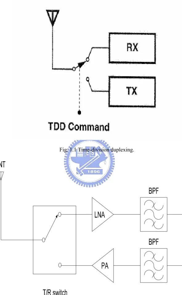
A high-quality microwave switch is a key building block of a RF front end for time-division duplexing (TDD) communication systems. The simplest case of multiple access is the problem of two-way communication by a transceiver, a function called “duplexing."
3
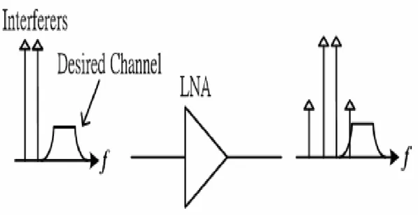
In old walkie-talkies, for example, the user would press the“talk"button to transmit while disabling the receive path and release the button to listen while disabling the transmit path. This can be considered a simple form of TDD, whereby the same frequency band is utilized for both transmit (TX) and receive (RX) paths, but the system transmits for half of the time and receives for the other half. Illustrated in Fig.1.1, TDD is usually performed fast enough to be transparent to the user. Transmit/receive (T/R) switches are the components directly connected witch the low noise amplifiers (LNA) and power amplifiers (PA) in the T/R modules, see Fig1.2.
Owing to low mobility, high substrate conductivity, low breakdown voltage, and various parasitic parameters of CMOS processes, it has many challenges to design CMOS switch to achieve high power-handling capability, low insertion loss, high isolation, and wide bandwidth.
4
Fig. 1.1 Time-division duplexing.
5
Chapter 2
Basic Concept in Switch Design
2.1 Effects of Nonlinearity
2.1.1 Intermodulation
While many analog and RF circuits can be approximated with a linear model to obtain their response to small signals, nonlinearities often lead to interesting and important phenomena. For simplicity, we limit our analysis to memoryless, time-variant systems and assume L + + + + ≈ ( ) ( ) ( ) ) ( 3 3 2 2 1 0 x t x t x t t y α α α α (2.1) If a sinusoid is applied to a nonlinear system, the output generally exhibits frequency components that are integer multiples of the input frequency. Ifx(t)= Acosωt, then
L + + + + = A t A t A t t y α α ω α ω α 3 3ω 3 2 2 2 1
0 cos cos cos
) ( (2.2) It can be written as L + + + + + + = A A A t A t A t t y α α α α ω α ω α cos3ω 4 2 cos 2 cos ) 4 3 ( 2 ) ( 3 3 2 2 3 3 1 2 2 0 (2.3)
The term with the input frequency is called the “fundamental"and the higher-order terms the “harmonics". We can observe that the amplitude of the nth harmonic consists of a term proportional to An.
6
In Eq. (2.3) this occurs ifα3<0.Written as
4 3 2 3 1 A α
α + , the gain is therefore a
decreasing function of A. In RF circuits, this effect is quantified by the “1-dB compression point,"defined as the input signal level that causes the small-signal gain to drop by 1 dB. If plotted on a log-log scale as a function of the input level, the output level falls below its ideal value by 1 dB at the 1-dB compression point, shown in Fig. 2.1.
7
When two signals with different frequencies are applied to a nonlinear system, the output in general exhibits some components that are not harmonics of the input frequencies. Called
intermodulation (IM), this phenomenon arises from multiplication of the two signals when
their sum is raised to a power greater than unity. It can assume that
x(t) = A1 cos
ω
1t + A2 cosω
2t (2.4) Apply this tone to (2.1), and y(t) can getL
4
4
4 3
4
4
4 2
1
4
4 3
4
4 2
1
4
43
4
42
1
+
α
+
+
α
+
+
α
+
+
α
=
3 2 1 3 2 2 1 2 2 1 1 0(
))
order
-third
)
(
(
))
(
order
-second
)
(
(
))
(
l
fundamenta
)
(
(
)
(
t
x
t
x
t
x
t
x
t
x
t
x
t
y
(2.5) Thus, 3 2 2 1 1 3 2 2 2 1 1 2 2 2 1 1 1 ) cos cos ( ) cos cos ( ) cos cos ( ) ( t A t A t A t A t A t A t y ω + ω α + ω + ω α + ω + ω α = (2.6)Expanding the left side and discarding DC terms and harmonics, it can obtain the intermodulation products:
t
A
A
t
A
A
)
2
cos(
4
3
)
2
cos(
4
3
:
2
2 1 2 2 1 3 2 1 2 2 1 3 2 1ω
ω
α
ω
ω
α
ω
ω
ω
→
±
+
+
−
(2.7)t
A
A
t
A
A
)
2
cos(
4
3
)
2
cos(
4
3
:
2
1 2 1 2 2 3 1 2 1 2 2 3 1 2ω
ω
α
ω
ω
α
ω
ω
ω
→
±
+
+
−
(2.8)Due to the difference between ω1 and ω2 is small, the components at 2ω1-ω2 and 2ω
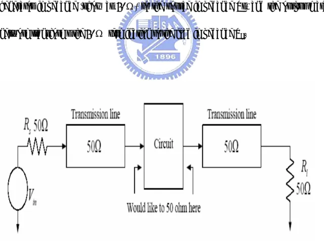
2-ω1 appear in the vicinity of ω1 and ω2. In a typical two-tone test, A1=A2=A, and the ratio of the amplitude of the output third-order products to α1A defines the IM distortion. Intermodulation is a troublesome effect in RF systems. As shown in Fig. 2.2, if a weak signal
8
accompanied by two strong interferes experiences third-order nonlinearity, then one of the IM products falls in the band of desired output if ω1 is close in frequency toω2 and therefore cannot be easily filtered out. The effect is that third-order nonlinearity can change the gain, which is seen as gain compression. And the two-tone (2ω1-ω2, 2ω2-ω1) are usually referred to as three-order intermodulation terms (IM3 products). [1]
9
2.1.2
The 1-dB Compression Point and Third-Order Intercept Point
If an amplifier is driven hard enough the output power will begin to roll off resulting in a drop of gain known as gain compression, and the phenomenon is showed as Fig. 2.3. The measurement of gain compression is given by the 1-dB gain compression point.
The 1-dB Compression Point:
As shown in Fig. 2.1, this parameter in one measure of the linearity of a device and is defined as the input power that causes a 1dB drop in the linear gain due to power compression.
When operating within the linear region of a component, gain through that component is constant for a given frequency. As the input signal is increased in power, a point is reached where the power of the signal at the output is not amplified by the same amount as the smaller signal. At the point where the input signal is amplified by an amount 1 dB less than the small signal gain, the 1 dB Compression Point has been reached. A rapid decrease in gain will be experienced after the 1 dB compression point is reached. If the input power is increased to an extreme value, the component will be destroyed.
10
Third-Order Intercept Point:
A third-order intercept point is another measure for weakly nonlinear systems and devices, for example receivers, linear amplifiers and mixers. It is based on the idea that the device nonlinearity can be modeled using a low order polynomial, derived by means of Taylor series expansion. The third order intercept point relates nonlinear products caused by the third order term in the nonlinearity to the linearly amplified signal.
The third-order intercept point is a theoretical point where the amplitudes of the fundamental tones at 2ω1-ω2 and 2ω2-ω1 are equal to the amplitudes of the fundamental tones at ω1 and ω2.
From (2.5), when ω1 = ω 2 → x1(t ) = x2(t) = xin ,the fundamental (F) of the third-order terms can be written as:
3 3 1 4 9 F = α xin + α xin (2.10) The linear component con be written as:
in
x
1
F = α (2.11)
Compared to the third-order intermodulation term ( 3 3 4 3
IM3 = α xin ), since the IM3 terms rises three times as the fundamental (60dB/decade to 20dB/decade) if xin is small, it can define a theoretical voltage (xin = vIP3 ) when these two tones will be equal:
1 4 3 3 1 3 3 3 = α α IP IP v v (2.12)
11 Therefore 3 1 3 3 2 α α = IP v (2.13)
As shown in Fig. 2.3, the intercept point is obtained by plotting the output power versus the input power on dB scale. The input power at this point is called the input third-order
intercept point (IIP3). If IP3 is specified at the output, it is called the output third-order intercept point (OIP3). [2]
12
Two curves are drawn, one for the linearly amplified signal at an input tone frequency, one for a nonlinear product. On a logarithmic scale, “x to the power of n"translates into a straight line with slope of n. Therefore, the linearly amplified signal will exhibit a slope of 1. A third order nonlinear product will increase by 3 dB in power, when the input power is raised by 1 dB. [2]
For instance, it has an output power called P1 at the fundamental frequency and an input power Pi called P3 at the IM3 frequency, and we know the IM3 terms have a slope 3 times as the fundamental terms (60dB/decade to 20dB/decade). Thus, when the units of X-axis and Y-axis are dBm, 1 P -IIP3 P -OIP3 i 1 = and IIP3 - P 3 P -OIP3 i 3 = (2.14)
Assume a device has power gain G, and G can be measured as :
i 1 P P IIP3 -OIP3 G = = − (2.15) So it can solve IIP3:
[
1 3]
i[
1 3]
1 P P 2 1 P G P P 2 1 P IIP3 = + − − = + − (2.16)13
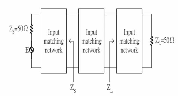
2.2 Impedance Matching
Consider the RF system shown in Figure 2.4. Here the source and load are 50Ω (a very popular impedance), as are the transmission lines leading up to the IC. For optimum power transfer, prevention of ringing and radiation, and good noise behavior, we need the circuit input and output impedances matched to the system. In general, some matching circuit must almost always be added to the circuit, as shown in Fig. 2.5. Figure 2.6 illustrates a typical situation in which a transistor, in order to deliver maximum power to 50Ω load, must have the terminations Zs and ZL. The input matching network is designed to transform the generator impedance (show as 50Ω) to the source impedance Zs, and the output matching network transforms the 50Ω termination to the load impedance ZL.
14
Fig. 2.5 Circuit embedded in a 50-Ω system with matching circuit.
15
Typically, reactive matching circuits are used because they are lossless and because they do not add noise to the circuit. However, using reactive matching components means that the circuit will only be matched over a range of frequencies and not at others. If a broadband match is required, then other techniques may need to be used. An example of matching a transistor amplifier with a capacitive input is shown in Figure 2.7. The series inductance adds an impedance of jωL to cancel the input capacitive impedance. Note that, in general, when an impedance is complex (R+jX), then to match it, the impedance must be driven from its complex conjugate (R-jX).
A more general matching circuit is required if the real part is not 50Ω. For example, if the real part of Zin is less than 50Ω, then the circuit can be matched using the circuit in Figure 2.8.
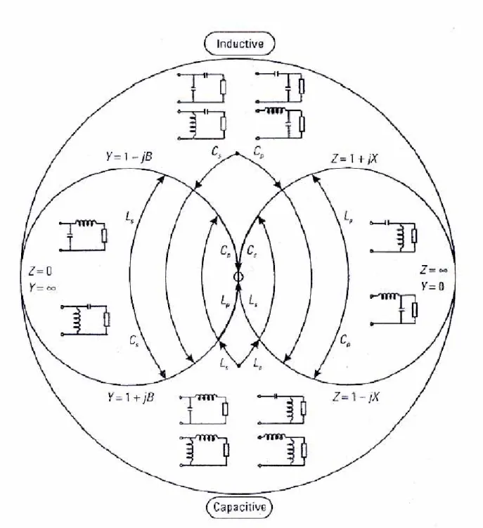
Series components will move the impedance along a constant resistance circle on the Smith chart. Parallel components will move the admittance along a constant conductance circle on the Smith chart. The input impedance of a circuit can be any values. In order to have the best power transfer into the circuit, it is necessary to match this impedance to the impedance of the source driving the circuit. The output impedance must be similarly matched. It is very common to use reactive components to achieve this impedance transformation, because they do not absorb any power or add noise. Thus, series or parallel inductance or capacitance can be added to the circuit to provide an impedance transformation.
16
With the proper choice of two reactive components, any impedance can be moved to a desired point on the Smith chart. There are eight possible two-component matching networks, also known as ell networks, as shown in Figure 2.9. Each will have a region in which a match is possible and a region in which a match is not possible.
In any particular region on the Smith chart, several matching circuits will work and others will not. This is illustrated in Figure 2.10, which shows what matching networks will work in which regions. Since more than one matching network will work in any given region, how does one choose? There are a number of popular reasons for choosing one over another.
1. Sometimes matching components can be used as dc blocks (capacitors) or to provide bias currents (inductors).
2. Some circuits may result in more reasonable component values.
3. Personal preference. Not to be underestimated, sometimes when all paths look equal, you just have to shoot from the hip and pick one.
4. Stability. Since transistor gain is higher at lower frequencies, there may be a low-frequency stability problem. In such a case, sometimes a high-pass network (series capacitor, parallel inductor) at the input may be more stable.
5. Harmonic filtering can be done with a lowpass matching network (series inductor, parallel capacitor). This may be important, for example, for power amplifiers. [2]
17
Fig.2.7 Example of a very simple matching network.
18
19
20
Chapter 3
How to Design Basic Switch
3.1 Introduction
In recent years, wireless communication systems have undergone explosive growth that is largely unanticipated. In time-division duplexing (TDD) communication systems, transmit-receive (T/R) switch plays an important role to control the RF signal flow to transmitter (TX) or receiver (RX). In the receive mode, T/R switch will receive the signal from antenna. Because the switch is in front of the low noise amplifier, insertion loss will influence noise figure of receive path directly. In the transmit mode, T/R switch need to handle the great power signal from transmitter in order to avoid signal distortion. Simultaneously, isolation can determine whether both signals may influence each other or not. Therefore, the key parameters of single pole double throw (SPDT) switch are insertion loss, power-handling capability and isolation.
Silicon-based CMOS technology has fast become one of the most favorable processes for RFICs due to its low cost and highly integrative capacity. Owing to low mobility, high substrate conductivity, low breakdown voltage, and various parasitic parameters of CMOS processes, it has many challenges to design CMOS switches to achieve low insertion loss, high isolation, wide bandwidth, and high power-handling capability.
21
3.2 Basic Concept
Some basic circuits of switch will introduce in this chapter. Traditional typology of T/R switch is a series type, see Fig.3.1. The equivalent circuit model of an on-state transistor is a small resistor. For the off-state transistor, it is represented as a small capacitor. When operating frequency increases, equivalent impedance will become smaller, see eq.3.1. Isolation will become worse between transmit and receive end.
C
j
Z
ω
1
=
(3.1)There are many references to improve isolation of switch such as resonant with shunt inductor [5], series-shunt type [6], T-shaped R-C-R circuit [7]. When resonant type operates in the center frequency, inductor and“off-state"transistor, which equivalent circuit is capacitor, become resonant circuit, see Fig3.2. This structure needs to use inductor as the same number as transistor. It will use large layout area to realize this circuit. Therefore, it is unsuitable to be realized.
Series–shunt type is shown in Fig.3.3, the function of shunt transistor is insert signal to ground. For this reason, it can improve isolation definitely. Therefore, this structure is used widely in designing T/R switch. When operating frequency increases, series-shunt type has the same problem with traditional series type. Signal loss on off-state path will become worse as frequency increasing.
22
shunt transistor. There are many ways to solve the power-handling capability issue. From the paper [8], it used stacked series transistors to share power, so power-handling capability can be improved.
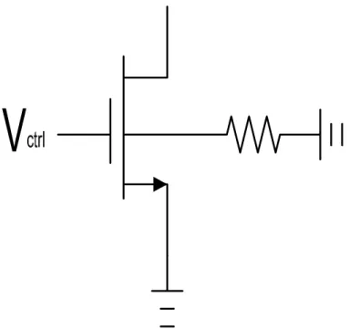
The switch uses an LC-tuned substrate biasing technique to dramatically improve the power-handling capability [9]. The body of transistor is series a resonant circuit with capacitance shunt inductance, see Fig. 3.4. It can improve power-handling capability in the specific frequency range. On the other hand, it can be used only on narrow band.
Body-floating technique is body series a large resistor about 5kΩ, see Fig.3.5. It has the same operating mode with LC-tuned substrate biasing technique, but it can improve power-handling capability in a wide band. Besides, it can also decrease insertion loss for on-state switch [10][11].
A 15-GHz T/R switch is reported in [13], the impedance matching network was employed to improve the linearity, while the isolation performance is degraded. The linearity can also be improved by using differential architectures [17], 3-dB linearity improvement can be obtained.
23
Fig.3.1 The series type of switch.
24
Fig. 3.3 The series-shunt type of switch.
25
26
3.3 Body-Floating Technique
The goals of SPDT performance are low insertion loss, high isolation and high power-handling capability.To improve the insertion loss, the substrate resistance RB should be either extremely large or close to zero. However, it is impossible to make RB zero due to the parasitic effect. Therefore, it is important to let RB be large enough. By using body-floating technique can reduce the parasitic effect.
In order to improve the power-handling capability of the CMOS switch, it can use the body-floating technique [10]. The circuit schematic of a shunt transistor is shown as Fig. 3.6(a). For the off-state transistor, it is represented as a small capacitor. Body to source and body to drain can be equivalent to the two back-to-back parasitic diodes. The equivalent circuit model on off-state is shown in Fig. 3.6(b).
In general, body connect to source type, the high input power signal will turn on the diode between body and drain. The diode can be equivalent to a small resistor. A small resistor will cause the current from ground to drain increasing quickly. The high current will change the input impedance of the transistor, and degrade the power-handling capability as shown in Fig. 3.6(c).
The equivalent circuit model of the off-state transistor with the body-floating technique , is shown in Fig. 3.6(d). The body of the transistor is connected to ground with a large resistor by using body-floating technique. The high input power signal will still turn on the diode
27
between body and drain. The diode also can be equivalent to a small resistor. But the resistor between body and ground is very large, the current from ground to drain will increase smoothly. For this reason, power-handling capability can be improved by using body-floating technique.
28
(a) (b)
(c) (d)
Fig.3.6. (a) Circuit schematic of shunt transistor, (b) the equivalent model in the off-state, (c) without body-floating technique, (d) with body-floating technique
29
3.4 Asymmetric-LDD MOS transistor for RF Circuit Design
The rapid technology evolution of Si MOSFET is beneficial for IC design with higher device speed and cost reduction. However, the low drain breakdown voltage of CMOS transistors restricts the use of CMOS for power amplifiers. This limitation for high voltage operation significantly reduces the maximum output power and efficiency for CMOS devices. To overcome the low breakdown voltage issue and improve the RF power performance, we use asymmetric-lightly-doped-drain (LDD) MOS transistor for high frequency RF power application.
This new asymmetric MOSFET is fully embedded in the conventional foundry logic process without any additional process step or extra cost. As technology evolution and down-scaling the Si MOSFET into sub-100 nm region, the performance of RF gain, cut-off frequency (ft), maximum oscillation frequency (fmax) and RF noise figure improve continuously but not the RF output power. This is originated from the lower source-drain breakdown voltage than that GaAs MESFET due to the smaller bandgap of 1.1eV than that of GaAs (1.42eV). The asymmetric-LDD MOS transistor that has higher drain breakdown voltage but also preserve high RF gain, ft and fmax for high frequency operation.
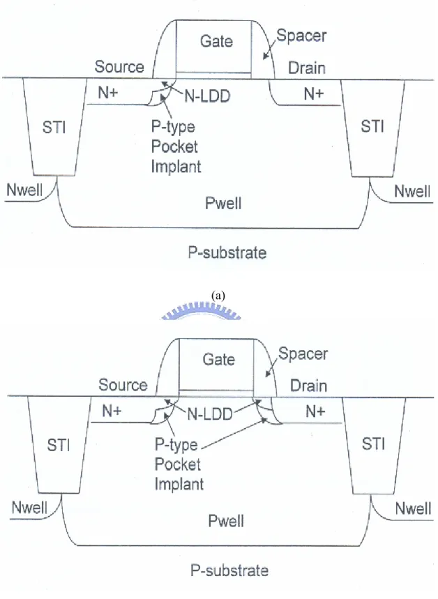
The structure comparison of (a) the new asymmetric-LDD MOS transistor and (b) conventional MOS transistor are shown schematically in Fig. 3.7. The LDD region at the drain size was removed that is the major difference to conventional MOS. This large
30
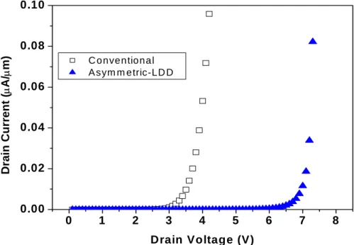
improvement of breakdown voltage is due to the designed wide depletion region beneath the spacer region and between the drain and substrate. In contrast the existing n+-LDD in conventional CMOS transistor just provides an electrically short path between inversion channel and drain. Such wide depletion region in the new design can support significantly larger reverse-biased drain voltage than conventional case. Figure 3.8 shows the comparison of DC drain breakdown voltage for conventional and asymmetric-LDD MOS transistor. For conventional MOS, the breakdown voltage is 3.6V. In sharp contrast, the breakdown voltage of asymmetric-LDD MOS is increased to 7.0V. So we can use the asymmetric-LDD MOS in our switch design to improve power-handling capability. [12]
31
(a)
(b)
Fig. 3.7 Device structure of (a) an asymmetric-LDD MOS transistor and (b) a conventional MOS transistor.
32 0 1 2 3 4 5 6 7 8 0.00 0.02 0.04 0.06 0.08 0.10 Drain Current ( µ A/ µ m) Drain Voltage (V) C onven tional A sym m etric-LD D
Fig. 3.8 Comparison of drain breakdown voltage for conventional and asymmetric-LDD MOS transistor.
33
Chapter 4
SPDT Circuit1 Design
4.1 Circuit1 Topology
Fig. 4.1 shows the circuit schematic. This circuit was designed with Agilent Advanced Design System (ADS), and implemented in TSMC’s 0.18µm RF CMOS technology. Due to
the different requirements in the receive mode and the transmit mode, the SPDT switch is designed to be asymmetric. The T/R switch was designed by series-shunt topology using body-floating technique and asymmetric-LDD MOS transistor.
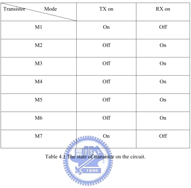
The devices of M1、M2、M3 are series transistors, and M4、M5、M6、M7 are shunt transistors which can improve the isolation of T/R switch. The signal is from ANT node to TX node or to RX node. Cbypass is on-chip bypass capacitor which is chosen to be as large as possible to provide ideal ac ground. It can isolate DC to avoid DC power consumption. The on-state transistor can be equivalent to a small resistor and the off-state transistor can be equivalent to a capacitor which is shown in Fig.4.2. The on-state and off-state of transistors are shown as Table 4.1. On-state transistor is biased at 1.8V and off-state transistor is biased at 0V. M4、M5、M6 use asymmetric-lightly-doped-drain (LDD) MOS which is our LAB developed MOS, see section 3-4. This large improvement of breakdown voltage is due to the designed wide depletion region beneath the spacer region and between the drain and substrate. Asymmetric-LDD MOS transistor can endure high voltage. The key point is the large bias
34
region on the transmitter path to improve the power linearity. Therefore, the higher drain breakdown voltage of asymmetric-LDD MOS transistor is used for the transmitter path. In this circuit, TX node is biased at 2.8V more than 1.8V in conventional MOS transistor. It can increase voltage swing, therefore improving the power-handling capability of T/R switch. Besides, the shunt transistors M4、M5、M6 and the series transistors M2、M3 use the body-floating technique. The body-floating technique is to keep the parasitic diodes from being forward bias under large input signals, hence, improving the linearity and power-handling capability of CMOS T/R switch, introduced in section 3-3. M2、M3 utilize stacked transistor configuration to improve the power-handling capability. But it will also make the insertion loss increasing on the receive mode. Due to the trade-off between the power-handling capability and the insertion loss, the two stacked transistors are selected to approach the optimum.
35 Transistor Mode TX on RX on M1 On Off M2 Off On M3 Off On M4 Off On M5 Off On M6 Off On M7 On Off
36
37
G
S
D
R
C
On-state
Off-state
38
4.2 Simulation and Measurement Result
The RF performance of the UWB CMOS T/R switch has been measured by using network analyzer and on-wafer probing system. The other path is terminated with 50ohm when on-state and off-state characteristics are measured for one path. The control voltage is 1.8V for on-state and 0V for off-state.
4.2.1 TX Mode
The signal from antenna to transmit mode is TX mode. Figure 4.3 shows the simulated and measured isolation of the SPDT switch on TX mode. The red line is simulation and the blue line is measurement result. The measured isolation of SPDT switch achieves 31.4dB. Figure4.4 shows the simulated and measured insertion loss on TX mode. The measured maximum insertion loss is 1.8dB. The return loss S11 and S22 on TX mode is small than -10dB, showed in Fig. 4.5 and Fig. 4.6. The power-handling capability achieves 28.7dBm, showed in Fig 4.7.
39
Fig. 4.3 Simulated and measured isolation on the TX mode.
40
Fig. 4.5 Simulated and measured S11 on the TX mode.
41
42
4.2.2 RX Mode
The signal from antenna to receive mode is RX mode. Figure 4.8 shows the simulated and measured isolation of the SPDT switch on RX mode. The measured isolation of SPDT switch achieves 20.0dB. Figure4.9 shows the simulated and measured insertion loss on RX mode. The measured maximum insertion loss is 4.1dB. The return loss S11 and S22 on RX mode is small than -10dB, showed in Fig. 4.10 and Fig. 4.11. The die micrograph of the asymmetric T/R switch using 0.18um standard CMOS process is shown in Fig. 4.12. The chip size is 0.325mm2. The effective circuit area without pads is only 0.11mm2.
43
Fig. 4.8 Simulated and measured isolation on the RX mode.
44
Fig. 4.10 Simulated and measured S11 on the RX mode
45
46
4.3 Summary
By the asymmetry series-shunt structure, an asymmetric-LDD MOS transistor, a body-floating technique, a high power-handling capability T/R switch is developed for UWB system application. Table 4.2 is the comparison of T/R switch performance. It shows highest power-handling capability by using asymmetric-LDD MOS transistor in this table. However, the disadvantage of this circuit is the higher insertion loss on RX mode. In the chapter5, the circuit2 has been redesigned to improve the insertion loss issue.
Reference Process Frequency
(GHz) Loss(dB) Isolation (dB) P1dB (dBm) Technology Chip area (mm2) [11] 0.18um CMOS 5.8 1.1 27 20 Body-Floating 0.2* [13] 0.13um CMOS 2~12 <1.1 >23 15 INT’s 0.25 0.9 0.97 >39 24.3 [14] 0.18um CMOS 2.4 1.1 >24 20.6 0.35um transistor by P-Si substrate 0.28 [15] 0.18um CMOS 3~10 <4.4 >27 20 Series-shunt 0.626 TX <1.8 TX >31.4 This work 0.18um
CMOS 3.1~10.6 RX <4.1 RX >20 28.7 Asymmetry MOS 0.325/0.11*
47
Chapter 5
SPDT Circuit2 Design
5.1 Circuit2 Topology
Fig. 5.1 shows the circuit2 schematic. The circuit2 was designed by series-shunt type using body-floating and asymmetric-LDD MOS technique. This work used four transistors. The devices of M1、M2 are series transistors, and M3、M4 are shunt transistors which can improve the isolation of T/R switch. The signal is from ANT node to TX node or to RX node.
Cbypass is on-chip bypass capacitor to provide ideal ac ground. It can isolate DC to avoid DC
power consumption. The on-state and off-state of transistors are shown as Table 5.1. The higher drain breakdown voltage of asymmetric-LDD MOS transistor M3 is used for the transmitter path. It can increase voltage swing, therefore improving the power-handling capability of T/R switch. Besides, the shunt transistor M3 uses the body-floating technique to improve power-handling capability. The body-floating technique was introduced in section 3-3.
48 Transistor Mode TX on RX on M1 On Off M2 Off On M3 Off On M4 Off On
Table 5.1 The state of transistor on the circuit2.
Fig. 5.1 The complete circuit schematic of the chip2.
49
5.2 Simulation Result
The signal from antenna to transmit mode is TX mode. Figure 5.2 shows the simulated the isolation of the SPDT switch on TX mode. The simulated isolation of SPDT switch achieves 26.2dB. Figure5.3 shows the simulated the insertion loss on TX mode. The simulated maximum insertion loss is 0.94dB. The return loss S11 and S22 on TX mode is small than -10dB, showed in Fig. 5.4. The power-handling capability achieves 30.1dBm, showed in Fig 5.5.
The signal from antenna to receive mode is RX mode. Figure 5.6 shows the simulated isolation of the SPDT switch on RX mode. The simulated isolation of circuit2 achieves 25.6dB. Figure5.7 shows the simulated insertion loss on RX mode. The measured maximum insertion loss is 1.29dB. The return loss S11 and S22 on RX mode is higher than -10dB, showed in Fig. 5.8. The layout diagram of the asymmetric T/R switch using 0.18um standard CMOS process is shown in Fig. 5.9. The chip size is 0.21mm2. The effective circuit area without pads is only 0.055mm2. Table 5.2 represents the simulated performance.
50 0 4 8 12 16 Frequency (GHz) -50 -45 -40 -35 -30 -25 -20 Is ol at io n ( d B ) Fequency=3.1 GHz Isolation=27.086 dB m1 m2 Frequency=10.6 GHz Isolation=26.215 dB
Fig. 5.2 Simulated isolation on the TX mode.
0 4 8 12 16 Frequency (GHz) -20 -16 -12 -8 -4 0 Ins e rti o n l o ss ( d B ) m1 Frequency=3.1 GHz Insertion loss=0.723 dB m2 Frequency=10.6 GHz Insertion loss=0.944 dB
51
Fig. 5.4 Simulated input and output return loss on the TX mode.
52 0 4 8 12 16 Frequency (Ghz) -50 -40 -30 -20 Is ol at io n ( d B ) m1 m2 Frequency=3.1 GHz Isolation=29.068 Frequency=10.6 GHz Isolation=25.690 dB
Fig. 5.6 Simulated isolation on the RX mode.
0 4 8 12 16 Frequency (GHz) -20 -16 -12 -8 -4 0 Ins e rt io n l o s s (d B ) m1 m2 Frequency=3.1 GHz
Insertion loss=0.844 dB Frequency=10.6 GHz Insertion loss=1.291 dB
53
54
Fig. 5.9 The layout diagram of circuit2.
TX“on”,RX“off” TX“off”,RX“on” Insertion loss (dB) Isolation (dB) P1dB (dBm) Insertion loss (dB) Isolation (dB) Post-sim <0.944 >26.215 30.1 <1.291 >25.691
55
5.3 Summary
By the series-shunt structure, an asymmetric-LDD MOS transistor, a body-floating technique, a high power-handling capability T/R switch is developed for UWB system application. Table 5.3 is the comparison of T/R switch performance. This work has highest power-handling capability in this table. This simulated result can prove that this circuit topology is useful for UWB system application.
Reference Process Frequency
(GHz) Loss(dB) Isolation (dB) P1dB (dBm) Technology Chip area(mm2) TX 1.5 TX 30 TX 28 2.4 RX 1.6 RX 15 RX 12.5 TX 1.5 TX 32 TX 28.5 [9] 0.18um CMOS 5.2 RX 1.6 RX 17 RX 11.5 Narrow band,LC-tuned Substrate Bias 0.56 [11] 0.18um CMOS 5.8 1.1 27 20 Body-Floating 0.2* 0.9 0.97 >39 24.3 [14] 0.18um CMOS 2.4 1.1 >24 20.6 0.35um transistor by P-Si substrate 0.28 [15] 0.18um CMOS 3~10 <4.4 >27 20 Series-shunt 0.626 0~10 0.5-0.7 >32 25.4-26.2 10~18 0.7-1.0 25-32 22.6-25.4 [16] 0.18um CMOS 18-20 1.0-2.5 25 19.8-22.6
Bias and Pattern Ground Shield Inductor 0.06* 0~10 0.9-1.7 >32 10~18 1.7 21-32 [17] 0.13um CMOS 18-20 1.7-2.0 21 25-30 Differential topology 0.17/0.027* TX<0.944 TX>26.215 This work (post-sim) 0.18um CMOS 3.1~10.6 RX<1.291 RX>25.691 30.1 Asymmetry MOS 0.21/0.055*
56
Chapter 6
Conclusion
A new fully integrated 0.18-um CMOS T/R power switch has been developed by asymmetric-LDD MOS transistor. By raising the drain operation voltage beyond conventional CMOS device, the RF power linearity of this new transistor is improved according to measurement and simulation results. Measurement result shows the highest P1dB compression point around 28.7dBm for UWB application .Moreover, this new asymmetric MOSFET is fully embedded in the conventional foundry logic process without any additional process step or extra cost. From the modified chip design simulation results, it shows low insertion loss and high-power handling capability. Therefore, asymmetric-LDD MOS transistor technique will be candidate in design T/R switch in the future.
57
Reference
[1] B. Razavi, “RF Microelectronics,” 1st ed. NJ, USA: Prentice-Hall PTR, 1998.
[2] John Rogers, Calvin Plett, Radio frequency integrated circuit design, Artech House, Boston, 2003.
[3] B. Razavi, “Design of Analog CMOS Integrated Circuits,” International ed. NY: McGraw Hill Co. 2001.
[4] G. Gonzalez, “Microwave Transistor Amplifiers Analysis and Design,” 2nd ed. NJ: Prentice-Hall, Inc. 1997.
[5] Hideki Takasu, Fumio Sasaki, Hisao Kawasaki, Hirokuni Tokuda, and Susumu Kamihashi, “W-band SPST transistor switches,"IEEE Microwave and Guided Wave Letters, vol. 6, no. 9, September 1996, pp. 315-316.
[6] Hieda M., Nakahara K., Miyaguchi K., Kurusu H., Iyama Y., Takagi T., and Urasaki S., “High-isolation series-shunt FET SPDT switch with a capacitor canceling FET parasitic inductance,"IEEE Transaction on Microwave Theory and Techniques, vol. 49, no. 12, December 2001, pp. 2453-2458.
[7] Nobuaki Imai, Akira Minakawa, and Hiroshi Okazaki, “Novel high-isolation FET switches,"IEEE Transactions on Microwave Theory and Techniques, vol. 44, no. 5, May 1996, pp. 685-691.
58
[8] Ohnakado T., Yamakawa S., Murakami T., Furukawa A., Taniguchi F., Ueda H. Suematsu N., and Oomori T., “21.5-dBm power-handling 5-GHz transmit/receive CMOS switch realized by voltage division effect of stacked transistor configuration with depletion-layer- extended transistors (DETs),"IEEE Journal of Solid-State Circuits, vol. 39, no. 4, April 2004, pp. 577-584.
[9] Niranjan A. Talwalkar, C. Patrick Yue, Haitao Gan, and S. Simon Wong, “Integrated CMOS transmit-receive switch using LC-tuned substrate bias for 2.4-GHz and 5.2-GHz applications,"IEEE Journal of Solid –State Circuits, vol. 39, no. 6, June 2004, pp. 863-870.
[10] Mei-Chao Yeh, Ren-Chieh Liu, Zuo-Min Tsai and Huei Wang, “ A miniature low-insertion-loss, high-power CMOS SPDT switch using floating-body technique for 2.4-and 5.8-GHz applications," IEEE Radio Frequency Integrated Circuits (RFIC)
Symposium, Long Beach, CA, Jun. 2005, pp. 451-454.
[11] Mei-Chao Yeh, Zuo-Min Tsai, Ren-Chieh Liu, Kun-You Lin, Ying-Tang Chang, and Huei Wang, “ Design and analysis for a miniature CMOS SPDT switch using body-floating technique to improve power performance, " IEEE Transactions on
Microwave Theory and Techniques, vol. 54, no. 1, Jan. 2006, pp. 31-39.
[12] Ming-Chu King, Tsu Chang, and Albert Chin, “ RF power performance of asymmetric-LDD MOS transistor for RF-CMOS SOC design,"IEEE Microwave and
59
Wireless Components Letters, vol. 17, no. 6, June 2007, pp. 445-447
[13] Zhenbiao Li and Kenneth K. O, “15-GHz fully integrated nMOS switches in a 0.13um CMOS process,” IEEE J. Solid-State Circuits, vol. 40, no. 1, Nov. 2005, pp.2323-2328 [14] Feng-jung Huang and Kenneth K. O,“Single-pole double-throw CMOS switches for
900-MHz and 2.4-GHz applications on p-silicon substrates, " IEEE J. Solid-State
Circuits, vol. 39, no. 1, Jan. 2004, pp. 35-41,
[15] K.-H Pao, C.-Y. Hsu, H.-R. Chuang, C.-L Lu and C.-Y Chen, “A 3-10GHz Broadband CMOS T/R Switch for UWB Applications”, 1st European Microwave Integrated
Circuits Conference, September 2006, Manchester, Uk, pp.452-455,
[16] Yalin Jin and Cam Nguyen, “Ultra-compact high-linearity high-power fully integrated DC-20-GHz 0.18μm CMOS T/R switch, ”IEEE Transactions on Microwave Theory
and Techniques, vol. 55, no.1, Jan. 2007, pp. 30-36
[17] Q. Li and Y. P. Zhang, “CMOS T/R Switch Design: Towards Ultra-Wideband and High Frequency,” IEEE J. Solid-State Circuits, vol. 42, no. 3, Mar. 2007, pp.563-570
[18] Y. C. Wu, E. Y. Chang, Y. C. Lin ,H. T. Hsu, S. H. Chen, W. C. Chen, W. C. Wu, L. H. Chu, and C. Y. Chang,“SPDT GaAs switches with copper metallized interconnects,"
IEEE Microwave and Wireless Components Letters, vol. 17, no.2, Feb. 2007, pp.
60