一個具有電流匹配之新電荷泵與低寄生雜頻之互補式金氧半5-GHz頻率合成器
108
0
0
全文
(2) 一個具有電流匹配之新電荷泵與低寄生雜頻 之互補式金氧半 5-GHz 頻率合成器. A Low Spurious Tones of 5-GHz CMOS Frequency Synthesizer with New Current-Match Charge Pump 研 究 生:許德賢. Student:Te-Hsien Hsu. 指導教授:吳重雨 教授. Advisor:Prof. Chung-Yu Wu. 國 立 交 通 大 學 電機資訊學院 電子與光電學程 碩 士 論 文 A Thesis Submitted to Degree Program of Electrical Engineering and Computer Science College of Electrical Engineering and Computer Science National Chiao Tung University In Partial Fulfillment of the Requirements for the Degree of Master of Science in Electronics and Electro-Optical Engineering June 2004 Hsinchu, Taiwan, Republic of China. 中華民國九十三年十二月.
(3) 一個具有電流匹配之新電荷泵與低寄生雜頻 之互補式金氧半 5-GHz 頻率合成器. 研究生 : 許 德 賢. 指導教授 : 吳 重 雨 教授. 國立交通大學電機資訊學院 電子與光電學程 (研究所) 碩士班. 摘要. 本篇論文是用台灣積體電路 0.18um CMOS 製程來實現一個 5-GHz 擁有低寄生雜頻之良好特性的頻率合成器。整個電路包含兩個具有 良好電流匹配的電荷泵,能有效的降低寄生雜頻。整個迴路所產生 的寄生雜頻能有效的抑制在小於 -69.52dBc。 此頻率合成器也搭配加上一個佈局面積較小的高速除法電路 (÷2),此架構能比一般使用電感所組成的除法器擁有較少的花費。 而這頻率合成器的輸出是以正交相位產生四個輸出,可應用在 IEEE 802.11a 之 RF 通訊協定的傳輸與接收器上! 整個電路最高工作在 5.62-GHz,且整個迴路最快能在 13.5uS 達到穩定。此頻率合成器的雜訊也壓制在小於 -107dBc。整個頻率 合成器工作在 1.8 伏特與可程式控制除法器工作在 1.4 伏特時所產 生的功率消耗小於 18.8mW。. I.
(4) A Low Spurious Tones of 5-GHz CMOS Frequency Synthesizer with New Current-Match Charge Pump Student: Te-Hsien Hsu. Advisor: Prof. Chung-Yu Wu. Degree Program of Electrical Engineering Computer Science National Chiao Tung University. Abstract. The thesis use TSMC 0.18um CMOS process to implement a 5-GHz frequency synthesizer that has perfect characteristic of low spurious tones. In this synthesizer which includes two perfect current-match of charge pump and they reduce spurious tones validly. The spurious sidebands at the center of adjacent channels are less than -69.52dBc. The frequency synthesizer collocate a small layout area of divide-by-2 divider, which structure of layout area and cost are smaller than other structure which like inductances loading type divider. The quadrature phase output of synthesizer can support IEEE 802.11a transceiver. The chip working frequency reach 5.62 GHz, and the loop settling time was small than 13.5uS. The frequency phase noise is restrained at -107dBc@1MHz. The chip total power is 18.8mW based on 1.4V power supply for program counter and swallow counter and 1.8V power supply for other block.. II.
(5) 誌. 謝. 首先,我要感謝我的指導教授 吳重雨教授並獻上我最誠摯的謝 意。 感謝吳老師在我研究所兩年半的期間,帶領著我一窺混合積體 高頻電路設計研究的博大精深與奧妙,並且在學習的旅程上不斷的 給予我指導與啟發。讓我受益良多! 其次,在這三年內,承蒙揚智科技的同意得以進修,在此感謝 幫助過我的同仁給予我的支持與鼓勵。特別是洪衛周部經理與朱允 康經理,因為有了他們兩位的支持才得以順利完成研究所的學業。 另外,我要感謝積體電路與系統實驗室的助理、學長、同學、 以及學弟妹們,特別是周忠昀及王文傑。感謝他們幫忙我解決課業 的疑問、處理學校的雜務以及協助實驗過程的種種,並且參與此篇 論文的討論並適時提供寶貴意見得以使其順利完成。 最後,我要感謝我最敬愛的父母、親愛的妻子、家人和朋友, 感謝他們給予我的關懷與照顧,使我在人生的過程裏得到快樂、健 康與幸福。 僅以此篇論文獻給所有關心我的每一個人。. 許德賢. III. 2004.12.
(6) CONTENTS. ABSTRACT (CHINESE)………………………………………....I. ABSTRACT (ENGLISH)…...........................................................II. ACKNOWLEDGEMENT….........................................................III. CONTENTS…..............................................................................IV. TABLE CAPTIONS…………………………………...….…….VII. FIGURE CAPTIONS…………………………………………..VIII. CHAPTER 1 1.1. INTRODUCTION...…….……………….….....1. BACKGROUND …..................................................................................1 1.1.1. HIGH FREQUENCY SYNTHESIZER…………………………..4. 1.1.2. THE CURRENT MISMATCH OF CHARGE PUMP INCREASE SPURIOUS TONES………………….……………….………….6. 1.1.3. THE INTERPLAY OF SETTLING TIME AND SPUR LEVEL.11. 1.2. REVIEW CURRENT MATCH CHARHE PUMP .................................12. 1.3. REVIEW 5-GHz FREQUENCY SYNTHESIZERS…...........................17 IV.
(7) 1.4. MOTIVATION……………………………………………………….....24. 1.5. MAIN RESOULT AND ORGANIZATION…........................................25. CHAPTER 2. CIRCUIT ARCHITECTURE AND SIMULATION RESULTS ………………....26. 2.1. 2.2. PHASE-LOCKED LOOP ARCHITECTURE..….................................27 2.1.1. S-DOMAIN MODEL OF PLL………………………………….27. 2.1.2. STEADY STATE PHASE ERROE ANALYSIS………………..31. 2.1.3. PLL NOISE SOURCE…………………………………………..33. CIRCUIT REALIZATION………………………………….…………35 2.2.1. CIRCUIT REALIZATION OF CURRENT-MATCH CHARGE PUMP………………….……………………………………….38. 2.3. 2.2.2. LOW PASS FILTER DESIN……………………..…….………46. 2.2.3. CIRCUIT REALIZATION OF QUADRATURE VCO…..……49. 2.2.4. CIRCUIT REALIZATION OF INTEGER-N DIVIDER……....56. 2.2.5. CIRCUIT REALIZATION OF PFD………..………………….61. SIMULATION RESULTS …………....................................................64 2.3.1. SIMULATION RESULTS OF QUADRATURE VCO…...........65. 2.3.2. SIMULATION RESULTS OF CURRENT-MATCH CHARGE PUMP…………………………………………………………..68. 2.3.3. SIMULATION RESULTS OF FRQUENCY DIVIDER….........71. 2.3.4. SIMULATION RESULTS OF PFD…........................................72. 2.3.5. SIMULATION RESULTS OF CLOSE LOOP V.
(8) SYNTHESIZER……………………..…………………………74 2.4. SUMMARY….........................................................................................76. CHAPTER 3 3.1. EXPERIMENTAL RESULTS……....…….… 77. CHIP ON BOARD TESTING AND SETUP…………………….…….78 3.1.1. MEASURE RESULTS OF VCO…...........................................80. 3.1.2. MEASURE RESULTS OF FREQUENCY SYNTHESIZER....81. 3.2. COMPARISON………………………………………………………...85. 3.3. DISCUSSION………………………….……………………………….86. CHAPTER 4. CONCLUSIONS AND FUTURE WORLKS..89. 4.1. CONCLUSIONS……………………….…….………………….….….89. 4.2. FUTURE WORKS …. ………………………….………......................90. REFERENCES ….......................................................................91. VI.
(9) TABLE CAPTIONS Table 1 Review 5GHz frequency synthesizer………………………………….19 Table 2 Divider parameters compared………………………………………...23 Table 3 Steady state phase error for various systems…………………………32 Table 4 PLL noise source………………………………………………………..33 Table 5 Final frequency synthesizer parameters……………………………...48 Table 6 The influences of Kvco and Vctrl in PLL ………………………………..55 Table 7 Program and swallow counter channel select setup mapping……….59 Table 8 Swallow counter setup mapping………………………………………60 Table 9 The summary of VCO simulation……………………………………..67 Table 10 The simulation results of rail-to-rail OP for charge pump type 2....69 Table 11 Compare the simulation results of charge pump type1 and type 2..70 Table 12 The simulation results summary of frequency synthesizer…...……76 Table 13 The measurement results of spurious tones………………………....81 Table 14 The measurement results of charge pump type 1 and type 2……....83 Table 15 Compare all characteristics of frequency synthesizer ……………...85 Table 16 Measurement results of synthesizer using active low pass filter…...87. VII.
(10) FIGURE CAPTIONS Fig. 1.1 Architecture for the 5-GHz CMOS WLAN receiver…………………..3 Fig. 1.2 Lower and Middle U-NII Bands: 8 Carriers in 200MHz Spacing……4 Fig. 1.3 Frequency synthesizer block diagram………………………………….5 Fig. 1.4 Effect of phase noise and spurious tones in a receiver………………...6 Fig. 1.5 PLL model for noise source that cause spurious tones………………..7 Fig. 1.6 (a) Sinking/Sourcing current in charge pump(b) Sinking/Sourcing current always mismatch unless charge pump output voltage is 1/2 power supply…………...……………….………………………….9 Fig. 1.7 Narrow bandwidth caused spurious tones……………………………10 Fig. 1.8 The voltage of Vctrl control VCO and general spurious tones………10 Fig. 1.9 Conventional charge pump circuits.......................................................13 Fig. 1.10 Perfect current-match characteristic of charge pump circuits….…14 Fig. 1.11 The structures of current-match charge pump circuit………….…..15 Fig. 1.12 Digital type of frequency synthesizer………………………………...17 Fig. 1.13 DLL type of frequency synthesizer……………….………………….18 Fig. 1.14 Divider structure (a) IFLD (b) TSCP (c) Pseudo-NMOS (d) SCL...23 Fig. 2.1 PLL block diagram ……………………………………………….……27 Fig. 2.2 VCO output frequency with control voltage curve……………..……28 Fig. 2.3 PLL AC linear model…………………………………………..………30 Fig. 2.4 Phase noise spectral for a PLL………………………………..……….34 Fig. 2.5 Frequency synthesizer function block of this thesis…………….…....36 VIII.
(11) Fig. 2.6 Current steering of charge pump …………………………………….38 Fig. 2.7 Non-idealities waveform of the charge pump switch ……………….40 Fig. 2.8 Non-idealities waveform of the charge pump current-mismatch ….40 Fig. 2.9 perfect current-match of charge pump circuit in this work (charge pump type 1) ……………………………………………………………41 Fig. 2.10 Wide input range OP. circuit ………………………………………..42 Fig. 2.11 Improve the current-match of charge pump circuit in this work (Charge pump type 2) ……………………………………………….43 Fig. 2.12 Rail-to-rail OP circuit in charge pump type 2 (OP1) ……………...44 Fig. 2.13 Current bias of charge pump in this work …………………………45 Fig. 2.14 OP circuit of charge pump in this work ……………………………45 Fig. 2.15 Type 2 third-order low pass filter …………………………………..48 Fig. 2.16 VCO circuit in this work ……………………………………………50 Fig. 2.17 On chip spiral inductors layout and equivalent circuit …………...51 Fig. 2.18 An N+/Nwell junction varactor …………………………………......52 Fig. 2.19 High Q structure of LC tank VCO …………………………………53 Fig. 2.20 LC tuned VCO model …………………………………………….....53 Fig. 2.21 The resistance simulation of LC tank in tuned VCO……………...54 Fig. 2.22 Pseudo-NMOS divider-by-two circuit (HDIV2) and input ac Coupling……………………………………………………………...56 Fig. 2.23 The ÷8/9 prescaler divider (Np = 8)………………………………....57 Fig. 2.24 The structure of divide-by-three stage ……………………………..58 Fig. 2.25 The structure of program and swallow counters ………………….59 IX.
(12) Fig. 2.26 The circuit of program and swallow counters ……………………...60 Fig. 2.27 The circuit of PFD in this work ……………………………………...61 Fig. 2.28 The PFD state diagram ………………………………………………62 Fig. 2.29 Four phase output waveforms of quadrature VCO………………...65 Fig. 2.30 The magnitude error of the quadrature VCO………………………65 Fig. 2.31 The simulation of VCO turning range………………………………66 Fig. 2.32 The frequency domain simulation of VCO………………………….66 Fig. 2.33 The phase noise of VCO………………………………………………67 Fig. 2.34 The simulation result of charge pump 2 tail current match waveforms…………………………………………………………......68 Fig. 2.35 The simulation result of current match charge pump type 2………69 Fig. 2.36 The gain distributed of rail-to-rail OP………………………………70 Fig. 2.37 Prescaler (÷8/9) and ÷2 simulated results…..………….……………71 Fig. 2.38 Program and swallow counter simulation results (channel 5)……..71 Fig. 2.39 The simulation result of PFD function………………………………72 Fig. 2.40 The simulation result of PFD locks state……………………………73 Fig. 2.41 Settling time of close loop 1 simulation of the synthesizer…………74 Fig. 2.42 Synthesizer loop 1 works at channel 8 that frequency is 5.32GHz...74 Fig. 2.43 Settling time of close loop 2 simulation of the synthesizer…………75 Fig. 2.44 Synthesizer loop 2 works at channel 8 that frequency is 5.32GHz...75 Fig. 3.1 The photo of the testing board in this work………………………......78 Fig. 3.2 The function block of the frequency synthesizer and testing environment………………………………………………………….....79 X.
(13) Fig. 3.3 The photo of main die in this work…………………………………....79 Fig. 3.4 The frequency and input turning range curves of VCO……….…….80 Fig. 3.5 The power level of spurious tones is channel 7 for charge pump2 and the power source is battery with regulator…………………………. .82 Fig. 3.6 The measurement result of feedback clock…………………….……..82 Fig. 3.7 The measurement result of settling time in close loop……………….84 Fig. 3.8 The measurement result of phase noise in 1 MHz offset…………….84 Fig. 3.9 The active low pass filter apply in charge pump output……………..87 Fig. 3.10 The variations of charge pump current and Vt……………………..88 Fig. 3.11 The current mismatch with Vt variation…………………………….88. XI.
(14) CHAPTER 1 INTRODUCTION. 1.1 Background. The growing of the wireless LAN market has generated increasing interest in technologies that will enable higher data rates and capacity than initially deployed system. There are much advantages of application in wireless LAN communication, so the entire world of the electronics industries researches high frequency circuit is very hard. Much kind of effect has devoted to the integration of such circuit in low cost technology in order to reach the goal. Being intended for mobile operations, the radio transceiver has a limited power budget. In high frequency synthesizer, the high power consumption is mainly due to the first stages of the frequency divider that often dissipates half of the total power. So, the structure of divide-by-2 stage affects power disputation and chip area seriously. Anyway, costs have been driven down by technology improvement and better design. The rapidly growing market and ever emerging new applications create a high demand for a low cost, low power, high portability transceiver solution. Many efforts are underway to increase the integration level of the transceiver. The ultimate goal would be a signal chip transceiver in a signal technology with a minimum number of off-chip components. This signal chip would act as an interface between the analog RF world and the digital baseband world. 1.
(15) In a conventional double conversion received signal spectrum is shifted down to the baseband in two steps. During the first step, a local oscillator signal at RF is mixed with the RF signal, shifting the signal to a fixed IF frequency. To achieve this, the RF LO needs to be tunable and the minimum frequency step must be smaller or equal to the channel spacing of the standard. To find ways to realize low-phase-noise synthesizers with low Q components is a major challenge. One approach is to use a wide synthesizer control bandwith to couple a noisy on-chip oscillator to a very low phase noise crystal more closely than a conventional narrow band PLL so that the output is more dependent on the clean reference. The phase noise contribution from the on chip oscillator to the output close to the carrier within the synthesizer control bandwidth is thus suppressed. And the spurious tone contribution from charge pumps up with down charge current not equal. This in turn requires the synthesizer maintain its phase noise and spurious tone performance in the presence of components with deliver significant current and voltage perturbations to both the substrate ground and supply. Some loop bandwidth of PLL designed in narrowband that ignore loop settling time to decrease spurious level is not our objective. As illustrate in Fig. 1.1, the RF front end need a high frequency synthesizer in transmitter and receiver to control mixer to generator internal carrier frequency. So designing a low phase noise and low spur frequency is very important. Charge pump up and down current equal to decrease spurious tone of the PLL path is important for this reason.. 2.
(16) Fig. 1.1 Architecture for the 5-GHz CMOS WLAN receiver. 3.
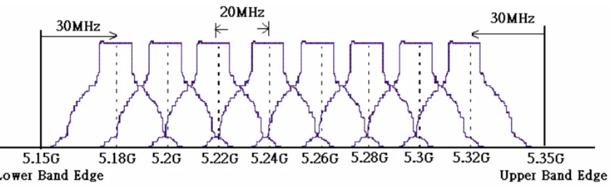
(17) 1.1.1 High frequency synthesizer. The growing demand for wireless connectivity has motivated the industry to evolve beyond today’s voice-based cellular services. Data-centric third-generation (3G) services now under development seek to provide substantially higher data rate, low noise interfere and wide channel bandwidth to supplement, and occasionally supplant, wired networks. At the same time, there is a constant desire to keep power consumption and layout size. Fortunately, continuing advances in integrated circuit technology have made possible the low-cost, compact implementation of transceivers capable of operating at 5-GHz carrier frequency with data rates competitive with established wired alternatives. The applications of wireless communication device include cellular phones and wireless local area networks, transmitting either voice or data. For voice, example includes GSM, CDMA, PCS and DECT. For data, there are 802.11 WLAN, Bluetooth and Home RF. As illustrate in Fig. 1.2, the 802.11a standard operates in the 5-GHz unlicensed national information infrastructure band. And there are eight channels be selected to carrier data.. Fig. 1.2 Lower and Middle U-NII Bands: 8 Carriers in 200MHz Spacing. 4.
(18) The frequency synthesizer illustrate in Fig. 1.3, usually implemented by a phase-locked loop (PLL), is one of the most critical blocks in terms of high frequency and average current dissipation since it operates extensively for both receiving and transmitting. The LO signals are generated by an integer-N frequency synthesizer. The loop employs a conventional phase-frequency detector (PFD) with the standard delay in the reset path to mitigate dead-zone effects arising from runt pulse. The PFD generating low-skew complementary representations of the UP and DOWN output that through low-pass filter to control VCO and generate the availability of accurate quadrature signals. The quadratue signals was divided by integer-N and backed to PFD.. Fig. 1.3 Frequency synthesizer block diagram. 5.
(19) 1.1.2 The current mismatch of charge pump increases spurious tones. The ideal output spectrum of a frequency synthesizer should be a single tone at the desired frequency in order to provide the reference frequency for frequency translation. A single tone in the frequency domain is equivalent to a pure sinusoidal waveform in the time domain. The random and systematic amplitude and phase deviations from the desired value produce energy in the frequencies other than the desired frequency. When this energy is mixed with the received RF signal or modulated base-band signal, undesired sidebands are created. In Fig. 1.4 shows the phase noise and spurious tones are the two key parameters to measure the quality of a frequency synthesizer.. Fig. 1.4 Effect of phase noise and spurious tones in a receiver. 6.
(20) In a receiver, the spurious tones and phase noise of the frequency synthesizer can mix with the undesired signal and produce noise in the desired channel. This reduced the sensitivity and selectivity of a receiver. Similarly, in a transmitter, the spurious tones and the phase noise of the frequency synthesizer can mix with the modulated base-band signal and produce undesired spectral emissions, increase adjacent channel interference, and reduce the modulation accuracy. The spurious tones of frequency synthesizer will interfere with adjacent channel in RF receiver and produce undesired spectral emission in RF transmitter. What noise source that will cause spurious tones in PLL and how does to suppress these noise? The source of spurious tone is either noise coupling VLP, or mismatch of charge pump current Icp, is depicted as Fig. 1.5.. Fig. 1.5 PLL model for noise source that cause spurious tones. If the cause is noise coupling, either power supply noise or substrate noise, to control voltage of VCO then spurious tones can be mitigated from floor plan of whole chip, power plan and guard ring. If the spurious tones are caused from. 7.
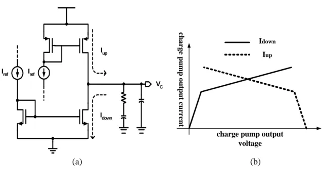
(21) mismatch of charge pump current then it can be mitigated from optimizing PLL loop or second order loop filter. The transfer function of Icp, due to current mismatch is. Wo / Icp = G ( s ) /(1 + β ( s ) ⋅ G ( s )) Η = s ⋅ Kvco ⋅ F ( s ) /( s + K ( s )). (1-1). Where. G ( s ) = Kvco ⋅ F ( s ) And β ( s ) = K φ /( s ⋅ 2 M ). (1-2). It is a low pass function and the frequency of Icp is at least 10 times large than K. Therefore optimizing K can attenuate the spurious tone. Briefly, we can mitigate the spurious tones, that noise source is VLF, by decoupling noise from power and substrate. And mitigates the spurious tones, that noise source is Icp, by loop filter optimized and make perfect current match of charge pump. When PLL is locked, reference and VCO frequency after divided by (2·M) is equal and in phase. Theoretically, charge pump circuit is high impedance and charge and discharge current is zero while PLL is locker, but in order to solve the dead zone problem, the charge and discharge current, which is a non-zero and equal value, still applies for a moment, the charge pump circuit remains high impedance. In practice, voltages stored on the loop filter will vary depend on the channel selected, thus the charge and discharge current will mismatch due to channel length modulation of MOS, as depicted in Fig. 1.6.. 8.
(22) Iref. Iref VC. Idown. charge pump output current. Iup. Idown Iup. charge pump output voltage. (a). (b). Fig. 1.6 (a) Sinking/Sourcing current in charge pump (b) Sinking/Sourcing current always mismatch unless charge pump output voltage is 1/2 power supply. Although the dead zone problem has been solved but there is a new problem be happened. Current difference between Iup and Idown flow into or from the loop filter while PLL is locked. The current mismatch of the charge pump generates a phase offset, which increase spurious tones in the PLL output. But if the PLL loop bandwidth design in narrow band application will decrease the power lever of spurious tones, as illustrated in Fig. 1.7, the delta V is the control voltage of VCO after to compare with low bandwidth and high bandwidth. Assume Kvco be fixed, the delta V ripple amplitude is small which cause VCO output phase offset small, too. So, the spurious tones power level in narrow bandwidth was batter than high frequency bandwidth. But narrow bandwidth caused loop settling time to become slow. The spur level is. Spur _ level ∝ Kvco ⋅ Vctrl / Wclk 9. (1-3).
(23) And the ripple affects the control voltage and spurious tones, as illustrated in Fig. 1.8.. Fig. 1.7 Narrow bandwidth caused spurious tones. Fig. 1.8 The voltage of Vctrl control VCO and general spurious tones. 10.
(24) 1.1.3 The interplay of settling time and spur level. Wireless LAN systems apply in the 5~6 GHz band, such as HiperLAN II and IEEE 802.11a, are recognized as the leading standards for high rate data transmissions. And the specification of loop settling time must small than 16uS. As mention in section 1.1.2, the power level of spurious tones is affected with charge pump current mismatch and loop bandwidth. In narrowband design, assume VCO’s gain Kvco is fixed and anyone of the Kf or Icp is decreased than settling time increase. In wideband design, assume VCO’s gain Kvco is fixed and anyone of the Kf or Icp is increased than settling time decrease. So, loop bandwidth and loop settling time are tradeoffs. Anyway, in narrowband design will increase the layout area of low pass filter that is not batter for SOC application. The PLL loop bandwidth is. K = Icp ⋅ Kf ⋅ Kvco / N. (N: Total divides value). (1-4). In this work, we choose large charge pump current to implement fast loop settling time.. 11.
(25) 1.2 Review current match charge pump. How does the synthesizer to decrease the level of spurious tones? The answer is focused to decrease the current mismatch of charge pump. Many structures of charge pump can solve the current mismatch problem after understand the reasons of spur be generated. Below listing, there are four reasons to make current mismatch in charge pump. (1) Sourcing current Iup and sinking current Idown are not mirrored from the same current source path. (2) Charge pump output range and channel length modulation cause charge pump current mismatch. (3) Charge sharing happen in the output of charge pump to effect the VCO input voltage. (4) The Up/Down signals from PFD to control the switches of the charge pump aren’t switching at the same time. A perfect current match of charge pump needs those four conditions to apply in low spur frequency synthesizer. Review the structures of charge pump in the past, the circuit of “Current switching charge pump [15]” and “Current steering charge pump [16]” shown in Fig. 1.9 (a),(b). From those schematic, the drain current of sinking and sourcing will vary with drain voltage of Ma and Mb. The sinking and sourcing current difference is relatively large when the voltage of loop filter is near supply voltage or ground in those conventional charge pump circuit. There are some conventional charge pumps circuits have been improved to 12.
(26) perfect current match on [17]-[18]. In Fig. 1.10 (a) [17], by using an error amplifier and reference current source, one can achieve a charge pump with good current matching characteristics. But the structure has some current mismatch problem when Ma and Mb have channel length modulation effect. In Fig. 1.10 (b) [18], it provided a charge pump with good current matching characteristics and a bootstrapping buffer forces the unused output in charge pump core to the same voltage as the main output [19]. The structure can’t work in high output voltage range application.. (a). (b) Fig. 1.9 Conventional charge pump circuits 13.
(27) (a). (b) Fig. 1.10 Perfect current-match characteristic of charge pump circuits Fig. 1.11 (a), the structure of charge pump has perfect characteristic of current-match. But the structure still has a problem about output voltage range cause current mismatch.. 14.
(28) (a). (b) Fig. 1.11 The structures of current-match charge pump circuit. 15.
(29) In [4], Fig. 1.11 (b) shows a conventional charge pump, the switches controlled by the UP and DN signals are directly connected between the current source transistors and output node. When the switches are turned off, the drain voltages of M1 and M2 are VDD and 0V, respectively. When one of the switches is turned on, the charges on the capacitors in the low pass filter. The structure of charge pump reduces this charge-sharing problem, but the up/down current has not to source from the same current path and it has serious problem of channel length modulation. We can see that current of M11 mirror from M5 and the current of M12 mirror from M8, but the current in M5 and M8 are not equal. Anyway, the circuits of charge pump from Fig. 1.9 to Fig. 1.11 can’t promise the current mirror can generate equal current to sink and source current of devices when the process has variation. Because the voltage of three thermals of current mirror device and sink/source current devices are not equal. In this work, there are two structures of charge pump circuit be implemented and compared at next chapter. Those charge pump circuit had perfect current match characteristic to decrease the power level of spurious tones.. 16.
(30) 1.3 Review 5-GHz frequency synthesizers. The role of the frequency synthesizer is to provide the reference frequency for frequency translation. There are many ways to implement a frequency synthesizer. We want the synthesizer to be able to generate a tunable frequency in the gigahertz range with low phase noise and low spurious tones using minimum power and small layout area. And the divide-by-2 divider dominated the power and layout area in frequency synthesizer. In synthesizer architecture, a direct digital frequency synthesizer is best known for its fast switching and very fine frequency resolution. It can also easily be integrated because no off chip components are required. But due to technology limitations, it takes large power consumption to synthesize very high frequency directly. A direct digital frequency synthesizer function block diagram show in Fig. 1.12. However, the spectral purity of the direct digital frequency synthesizer is limited by the DAC speed and resolution because the finite resolution in quantization leads to inaccurate representation of the sinusoid and hence spurious outputs. And high power consumption is needed for high frequency operation.. Fig. 1.12 Digital type of frequency synthesizer. 17.
(31) Recently a new approach to a frequency synthesizer using a Delay-Locked Loop has been proposed [5]. A DLL is a PLL with the voltage controlled oscillator replaced by a voltage controlled delay line. Fig. 1.13 shows the block diagram of a frequency synthesizer with a DLL core. The advantage of the DLL based frequency synthesizer is that the jitter dose not accumulates from cycle as in the ring oscillator voltage and thus lower phase noise at close-in frequencies can be achieved. This approach is amenable to the integration of the frequency synthesizer because no high Q tank is needed.. Fig. 1.13 DLL type of frequency synthesizer. Frequency synthesizer is to play the role of frequency conversion in RF front end circuit. It can be programmed to produce an exact frequency for up or down frequency. The greater parts of PLL-based researches are how does to decrease the effect from noise source. Because, noise effected the PLL’s characteristic very. 18.
(32) critical. We know the PLL noise source comes from “Phase Frequency Detector” and “Voltage Control Oscillator” and there are many technologies to solve low noise issue. PLL base frequency synthesizer using charge pump type has some advantages about low power and low noise. So, there are three papers using the structure to implement 5-GHz frequency synthesizer and be presented in IEEE journal of solid-state circuits. In table 1, the parameters of those researches are showed up.. [1]. [2]. [4]. Process. 0.24um. 0.25um. 0.25um. Current match CP. NO. N.A. YES. Loop bandwidth. 280KHz. 30KHz. 250KHz. Spurious tones. -45dBc. -70dBc. -69dBc. Settling time. N.A.. 100uS. N.A.. Charge pump current. 50uA. 50uA. 50uA. Power supply. 1.5V / 2V. 2.5V. 1.5V. Total power. 25mW. 13.5mW. 23mW. Chip size. 1.6mm². 0.55mm². N.A.. Off-chip low-pass-filter. No. Yes. Yes. Table 1 Review 5GHz frequency synthesizer. In [1], the power consumption of the synthesizer is significantly to reduce by using a tracking injection-locked frequency divider (ILFD) as the first frequency divider in the PLL feedback loop. On-chip spiral inductors with patterned ground shields are also optimized to reduce the VCO and ILFD power. In [2], the adoption of dynamic dividers in CMOS PLL for multi-gigahertz. 19.
(33) applications allows to reduce the power consumption substantially without impairing the phase noise and the power supply sensitivity of the PLL. The [2] had minimum spurious tones but loop settling time was too slow. The [2] had perfect power dissipation and small layout area but the loop bandwidth designed in 30 KHz. In [4], a new charge-pump circuit is developed to reduce the current glitch at the output node. By incorporating a voltage doubler, the voltage dynamic range at the charge-pump output and thus the VCO control voltage range are increased. In divide-by-2 architecture is very important in multi-gigahertz synthesizer; there are many ways to implement high speed divider. This work needs a high speed, smaller layout area and low power dissipation pre-divider between VCO and dual-modulus prescaler to gate 5.1GHz ÷2 ~ 5.3GHz ÷2 clock. So, the ÷2 divider must operate at full speed and differential signals from VCO output frequency. Conventionally, programmable dividers are implemented using a high speed dual-modulus prescaler along with low-speed programmable counters, which implement arbitrary division factors by “swallowing” pulses [7]. In [8], an asynchronous divider is presented in which pulse swallowing is accomplished by switching between different output phases of a ÷2 stage implemented using a master-slave flip-flop. The elimination of high-speed feedback loops around multiple flip-flops that would be present in a dual-modulus prescaler and reduced load on the VCO result in a higher maximum speed of operation and lower power consumption in a given technology. The high power consumption is mainly due to the first stage of the frequency divider that often dissipates half of the PLL total power. 20.
(34) The block most difficult to design is the first ÷2 stage, which should operate at 5.3GHz or more. Fig. 1.14 (a) to (d) shows some published latches intended for high speed operation. Fig. 1.14 (a) shows the schematic of the voltage controlled Injection-Locked Frequency Divider (ILFD) used in the frequency synthesizer. The incident signal (the VCO output) is injected into the gate of M3 and is delivered with a sub-unity voltage gain to Vx, the common source connection of M1 to M2. Transistor M4 is used to provide a symmetric load for the VCO. The signal is fed back to the gates of M1 and M2 and is summed with the incident signal across the gates and source of M1 and M2. As mentioned earlier the largest practical inductance L maximizes the locking range. However, reduction of power consumption demands maximization of the LQ product. The inductor has its largest value when the total capacitance that resonates with it is minimized. To reduce its parasitic bottom plate capacitance the inductor should be laid out with narrow topmost metal line.. So, this divider needed large. layout area and high cost. Both a conventional CMOS latch and a single-phase latch is TSCP. As illusion in Fig. 1.14 (b), its bandwidth had been dominated too slowly for our purposes they have a large input capacitance due to the parallel connection of PMOS and NMOS gates. Due to its lower mobility and larger threshold voltage, the PMOS transistor contributes little to the current drive and much to the capacitances, considerably slowing down the circuit. The latch proposed uses TSCP in the clock path that 25% duty cycle of the output signals is less convenient for phase switching. Another disadvantage of this structure is not differential signals path, but its layout area is 21.
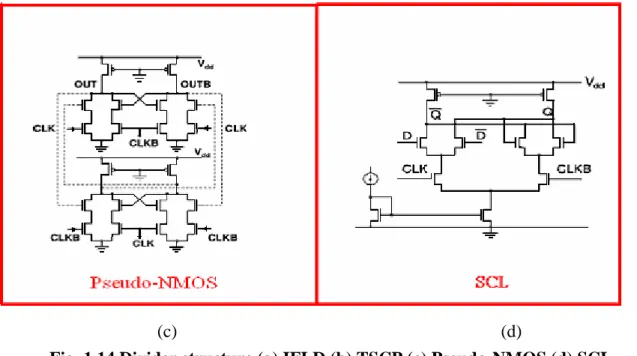
(35) very small. The source-coupled latch Fig. 1.14 (d) has a reduced output swing that facilitates high speed, but due to the stacking of many devices it cannot be accommodated in the intended low supply voltage. The SCL structure allows higher operating frequency, but burns more power. Fig. 1.14 (c) shows a Pseudo-NMOS D-flip-flop (DFF) whose outputs are connected back to its inputs (show in dashed lines) to form a ÷2 stage. NAND gates are used to form the latch since they enable a compact layout where node parasites can be minimized. Form simulations, the ÷2 circuit were found to operate satisfactorily over process and temperature variations at 6GHz while operating from a 1.8V supply and TSMC 0.18um process. And the ÷2 circuit’s layout area was small than Fig. 1.14 (a), (b) and (d).. (a). (b). 22.
(36) (c). (d). Fig. 1.14 Divider structure (a) IFLD (b) TSCP (c) Pseudo-NMOS (d) SCL. The four types of dividers were being compared about power consumption and layout area. The IFLD structure has maximum layout area more than other but it has least power consumption. The SCL structure has maximum power consumption more than other. Anyway, the table 2 has some parameters about those dividers.. [1]. [2]. [3]. [4]. Divider Structure. ILFD. TSCP. Pseudo-NMOS DFF. SCL. Power Supply. 1.5V. 2.5V. 2.5V. 1.5V. 0.24um. 0.25um. 0.25um. 0.25um. 0.186mm². 0.05 mm². 0.09 mm². 0.12 mm². 0.8mW. 6.25mW. 26mW. 10.5mW. Process Layout Area Divider Power. Table 2 Divider parameters compared Anyway, the low spur, low power consumption, small layout area and fast settling time are our design feature. In the work, those characteristics are implemented. 23.
(37) 1.4 Motivation. In RF transceivers, frequency synthesizer is one of the key components. Modern digital wireless system applications have demands on stringent specification, such as narrow channel spacing, large output power, high sensitivity and low bit error rate. So, a frequency synthesizer must have several advantages like low phase nose, low spur, fast setting time, lower power consumption and small layout area. How does to design a high frequency, fast settling time and low phase noise synthesizer? Several import circuit to increase performance for synthesizer be present in this work. For example: a perfect current matching charge pump decrease spur noise, a 5-GHz of quadrature output voltage control oscillator, high speed and small layout area divider and programmable integral N feedback divider. All the blocks have been researched, designed, simulated and testing in this work. Therefore, this thesis focuses on implementing the new circuit of current-steering charge pump, which incorporates with concept of perfect current matching. The new circuit of charge pump suffers no program of clock feed through and charge sharing, and has the perfect current matching characteristics. It is implemented in 5GHz CMOS frequency synthesizer.. 24.
(38) 1.5 Main results and organization. This thesis implements a new perfect current match of charge pump circuit in a 1.8V and 5GHz 0.18um CMOS frequency synthesizer. The spurious sidebands at the center of adjacent channels are less than -69.52 dBc. The PLL has a bandwidth of 250 KHz and a phase noise of -107 dBc at 1MHz. The PLL loop settling time is 13.5uS. The total power consumption is 20.8mW based on 1.8V power supply. And the total power consumption is 18.8mW based on 1.8V power supply with 1.4V power supply for PFD, program counter and swallow counter. The thesis is organized as follows. In chapter 2, the fundamentals of frequency synthesizer include the synthesizer architecture, reason, circuit, simulation results and their advantages and disadvantages are discussed. In chapter 3, presents experimental results, compared the results and discussion. In chapter 4, concludes the thesis with a summary and future work.. 25.
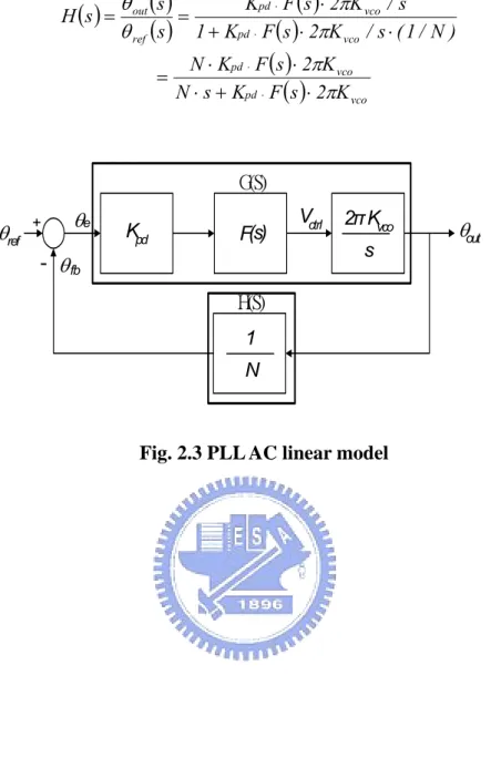
(39) CHAPTER 2 CIRCUIT ARCHITECTIRE AND SIMULATION RESULTS. In the previous chapter that propose wideband PLL architecture to implement a high performance frequency synthesizer with noisy on-chip components. In the chapter that also discusses the PLL design fundamentals, optimization of the loop bandwidth and pointed out the optimization of the loop bandwidth depends on the noise spectrum of each individual noise source. The important of the discusser are the structure of the current match charge pump and high speed frequency divider is chosen which has the trade off about power dissipation and layout area. Anyway, in this chapter the circuit design of each block in a PLL will be discussed. The most important block is the integrated quadrature VCO and perfect current match charge pump. And the phase/frequency detector, loop filter, and frequency divider are also important in realizing a high performance frequency synthesizer. So, architecture of every block will be analysis, design and simulate detail.. 26.
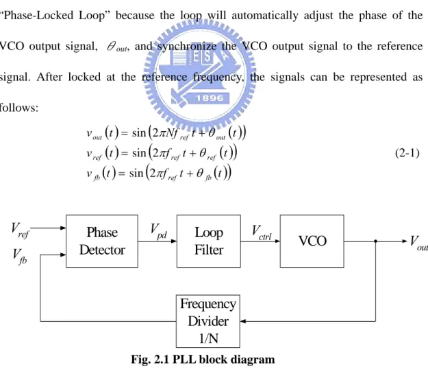
(40) 2.1 Phase-Locked Loop Design Fundamentals. 2.1.1 S-Domain model of PLL. The majority of all PLL design problems can be approached using the Laplace transform technique. All operating conditions are considered and evaluated. The Laplace transform is valid only for positive real time linear parameters; thus, its use must be justified for the PLL which includes both linear and nonlinear functions. Fig. 2.1 shows the basic block diagram of a PLL. The circuit is called a “Phase-Locked Loop” because the loop will automatically adjust the phase of the VCO output signal, θout, and synchronize the VCO output signal to the reference signal. After locked at the reference frequency, the signals can be represented as follows: v out (t ) = sin (2π Nf ref t + θ out (t )) v ref (t ) = sin (2π f ref t + θ ref (t )). (2-1). v fb (t ) = sin (2π f ref t + θ fb (t )). Vref Vfb. Phase Detector. Vpd. Loop Filter. Vctrl. VCO. Vout. Frequency Divider 1/N Fig. 2.1 PLL block diagram. The frequency divider divides both of the VCO frequency and phase by a factor. 27.
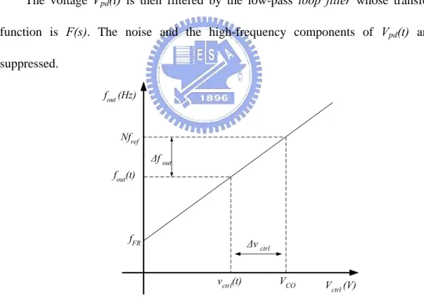
(41) N, thus. θ. fb. (t ) = θ. (t ). out. (2-2). N. The phase detector gives an output voltage proportional to the phase difference between the reference signal and the feedback signal:. (. ). v pd (t ) = K pd θ ref (t ) − θ fb (t ). (2-3). There Kpd is the phase detector gain and its unit is V/rad. The voltage Vpd(t) is then filtered by the low-pass loop filter whose transfer function is F(s). The noise and the high-frequency components of Vpd(t) are suppressed. fout (Hz). Nfref ∆f out fout(t). fFR. ∆v ctrl vctrl(t). VCO. Vctrl (V). Fig. 2.2 VCO output frequency with control voltage curve.. As shown in Fig. 2.2, the control voltage Vctrl determines the VCO output frequency. The relation between the VCO frequency and the control voltage can be written as 28.
(42) f out (t ) = f FR (t ) + K vco ⋅ v ctrl (t ). (2-4). There fFR is the “free running” frequency which denotes VCO oscillation frequency when Vctrl = 0 and Kvco is the VCO gain in units of Hz/V. Further, fout can also be written as. f out (t ) = Nf ref (t ) + ∆f out (t ). = Nf ref (t ) + K vco ⋅ (vctrl (t ) − VCO (t )). (2-5). = Nf ref (t ) + K vco ⋅ ∆vctrl (t ). There Vctrl is the VCO control voltage corresponding to the locked frequency. Nfref . Because frequency is the derivative of phase, the excess phase θ out in equation. (2-1) can be expressed as. θ out (t ) = 2π ∫ ∆ f out dt = 2πK vco ∫ ∆v ctrl (t )dt. (2-6). Taking the Laplace transform, the following result can be obtained. θ out (s ) =. 2πK vco ⋅ ∆Vctrl (s ) s. (2-7). The transfer function of the VCO is. θ out (s ) 2πK vco = ∆Vctrl (s ) s. (2-8). An ac linear model of the PLL now can be shown in Fig. 2.3. The phase transfer function of the PLL is. 29.
(43) H (s ) =. θ out (s ) Kpd ⋅ F (s ) ⋅ 2πK vco / s = θ ref (s ) 1 + Kpd ⋅ F (s ) ⋅ 2πK vco / s ⋅ ( 1 / N ). (2-9). N ⋅ Kpd ⋅ F (s ) ⋅ 2πK vco = N ⋅ s + Kpd ⋅ F (s ) ⋅ 2πK vco. G(S). θref. +. θe. Kpd. F(s). - θfb. Vctrl. 2πKvco. s. H(S) 1 N. Fig. 2.3 PLL AC linear model. 30. θout.
(44) 2.1.2 Steady state phase error analysis. Various inputs can be applied to a system. Typically, these include step position, velocity, and acceleration. The response of type 1, 2, and 3 systems will be examined with the various inputs. In Fig. 2.3 θ e represents the phase error that exits in the phase detector between the incoming reference signalθref and the feedback θout. In evaluating a system, θe must be examined in order to determine if the steady state and transient characteristics are optimum and/or satisfactory. The transient response is a function of loop stability and is covered in the next section. The steady state evaluation can be simplified with the use of the final value theorem associated with Laplace. This theorem permits finding the steady state system errorθe resulting from the inputθref without transforming back to the time domain. Simply stated. Lim [θ (t )] = lim [s θ e (s )]. (2-10). Where. θe(s ) = θref (s ) /(1 + G (s ) ⋅ H (s )). (2-11). The input signal θref is characterized as follows: Step position: θref (t) = Cp , t ≧ 0 Or, in Laplace notation: θref (s) = Cp / s. There Cp is the magnitude of the phase step in radians. This corresponds to shifting the phase of the incoming reference signal by Cp radians: 31.
(45) Step velocity: θref (t) = Cv · t, t ≧ 0 Or, in Laplace notation: θref (s) = Cv / s² The Cv is the magnitude of the rate of change of phase in radians per second. This corresponds to inputting a frequency that is different than the feedback portion of the VCO frequency. Thus, Cv is the frequency difference in radians per second seen at the phase detector. Step velocity: θref (t) = Ca · t², t ≧ 0 Or, in Laplace notation: θref (s) = 2 · Ca / s³ The Ca is the magnitude of the frequency rate of change in radians per seconds per second. This is characterized by a time variant frequency input. Similarly, applying the three inputs into type 1, 2 and 3 systems and utilizing the final value theorem, the following table 3 can be constructed to show the respective steady state phase errors. So, we chose type 2 and four order system in this work.. Step position Step velocity Step Acceleration. Type 1 Zero Constant Continually Increasing. Type 2 Zero Zero Constant. Type 3 Zero Zero Zero. Table 3 Steady state phase error for various systems. 32.
(46) 2.1.3 PLL noise source. Any noise in the circuit or environment will create phase disturbance. In Fig. 1.4, a non-ideal frequency synthesizer spectrum is show. It is no longer a single frequency tone but rather a smeared version. The energy under the skirt is phase noise. Sometimes the energy is concentrated at frequencies other than the desired frequency, appearing as a spike above the skirt. This energy is due to a spurious tone. Phase noise and spurious tones are the two key performance parameters of a frequency synthesizer. The PLL transfer function is easer to define from Fig. 2.3. T(s) = G(s) / (1 + G(s) · H(s)). (2-12). G(s) = Kpd · Kvco · F(s) / s. (2-13). H(s) = 1/N. (2-14). Below is table 4 showing various noise sources and the transfer functions that multiply each one.. Source. Transfer Function. Input Reference. G(s) / (1 + G(s) · H(s) ). Phase Detector. (1 / Kpd) · [(1 + G(s) · H(s) ) ]. VCO. 1 / (1 + G(s) · H(s) ). N divider. G(s) / (1 + G(s) · H(s) ). Table 4 PLL noise source It should be apparent that the phase detector noise, input reference noise, and N divider noise all contain common factor T(s) in their transfer functions. For. 33.
(47) this reason, all of these noise sources will be referred to as in band noise source. But the VCO noise distribute in high frequency band. That the in band sources dominate within the loop bandwidth and the VCO noise dominates outside of the loop bandwidth. This can be seen in Fig. 2.4. The phase noise measured at an offset that is close to the carrier is basically independent of loop bandwidth, provided that the loop bandwidth is sufficiently wide to eliminate the VCO noise. However, the phase error is more dependent on the loop bandwidth. To theoretically design for the lowest phase error, this means that one needs to design such that VCO noise contribution at loop bandwidth is equal to the total noise contribution from the other source noise at bandwidth. If the VCO is noisily relative to the PLL, than this number would be smaller, and if the PLL is noisily relative to the VCO, than this number would be large.. POWER PLL in band noise sources dominate. Phase noise in dBC. VCO noise dominate here. FREQUENCY. Fig. 2.4 Phase noise spectral for a PLL. 34.
(48) 2.2 Circuit realization. A Phase-Locked-Loop-Based frequency synthesizer with narrow loop bandwidth is the most commonly used techniques due to its high performance, namely, low phase noise and low spurious tones. But the need for off chip high-Q components is not amenable to the integration of the synthesizer. We used TSMC 0.18um process to implement the frequency synthesizer that has fast settling time and high Q devices on-chip. And the on-chip components are difficult to increase Q value more than off chip high Q components. So, the VCO’s turning range and gain (frequency over control voltage) curve is hard to control! First, we must to design a VCO before to design other block of frequency synthesizer. Because many key parameters like “VCO output frequency”, “VCO turning range” and “VCO gain curve (Kvco)” affect the all loop of properties seriously. And a frequency synthesizer loop characteristic determine from these key parameters. A “Phase-Locked-Loop” is a loop which locks the output phase or frequency to an accurate reference. In Fig. 2.5 shows the function block diagram of this work. A voltage-controlled oscillator generates an output waveform at a frequency set by the control voltage Vctrl. The Phase/Frequency Detector (PFD) compares the phase and frequency of a divided reference frequency Fref with the divider output phase and frequency. When the loop is locked, the PFD sees two identical waveforms at its inputs and Fout equals to N times of Fref. For some reason Fref > Fb, Vctrl goes up and the VCO output frequency increase. Vice versa, if Fref < Fb, Vctrl goes down and VCO 35.
(49) output decreases. A loop filter (LPF) is used to stabilize the loop by introducing zeros and poles into the loop. In this work include two perfect current match charge pumps to decrease spurious tones power level.. Fig. 2.5 Frequency synthesizer function block of this thesis. A typical PLL-based Frequency synthesizer comprises both high and low frequency blocks. The high frequency blocks, mainly the VCO and first stage of the frequency dividers, are main power consuming blocks, especially in a CMOS implementation. Anyway, several important design considerations about design frequency synthesizer in this these. One, the VCO input control voltage range must to collocate with charge pump output voltage range. In order to decrease spurious noise, charge pump driving and sourcing currents must be equal. So the cascode structure is used in this design to decrease MOS λ effect. The current mode LPF. 36.
(50) maybe can be used but buffer input offset must low enough. Two, the high frequency ÷2 divider input signal must to AC couple from VCO output. Three, the quadrature VCO output signals need to add buffer to driver out for easy testing. Five, the signal from program counter feedback to PFD and add some buffer to drive to PAD. Other design considerations will be discussed in this chapter every sub-chapter.. 37.
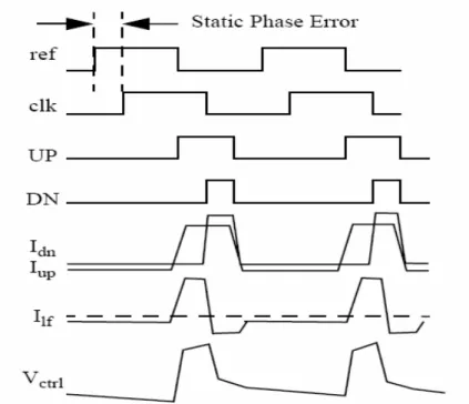
(51) 2.2.1 Circuit realization of current-match charge pump. In cellular applications, narrow loop bandwidth is desired in order to minimize the spectral components due to spurious tones in the output spectrum. So, charge pump is a low frequency block and the current of driving and sourcing to low-pass-filter (LPF) equal each other is very important. The spurious tones are generated because different currents of driving and sourcing to drive LPF. In this work has two perfect current matching charge pump circuits be implemented that will be compared at following. A simple implementation of the charge pump based on the current steering concept is shown in Fig. 2.6. Different UP and DN signals from the phase/frequency detector (PFD) are used to steer the current one way or the other in the differential pair in the charge pump.. Ip UP fref fb. Ilf C. PFD DN. Ip. F(s). Fig. 2.6 Current steering of charge pump. There are several non-idealities resulting in a non-zero static phase error and 38.
(52) creation of spurious tones. The top leakage current may not equal the bottom leakage current at up and down turn on together, resulting a net charge flowing in or out of the loop filter in one comparison period. In the PLL locking condition, the net charge must compensated by a different on-time of the two switches. For example, if Ip leakage is small than In leakage, the UP signal must occur slightly earlier than the DN signal to compensate for the net charge flow out of the loop filter. This means the. reference edge should come slightly earlier than VCO edge if we assume the PFD is ideal. The mismatch between the leakages is one form of static mismatch. Another form of the static mismatch is the DC current level difference when both switches are on. The effect is the same as in the case of leakage current mismatch. The switch has different finite switching on or off time is dynamic mismatch. Both dynamic and static mismatch result in net charge flows in or out of the loop filter periodically, at the rate of the comparison frequency. The result, the control voltage has a ripple at the comparison frequency, which modulates the VCO frequency and generates spurious tones at multiples of the comparison frequency away from the carrier. Fig. 2.7 shows the waveforms of the LPF with non-idealities and we can cancel the effect is delay balance in up and down path of PFD layout. And Fig. 2.8 shows the control voltage of VCO at up (UP) and down (DN) current mismatch and we can decrease the effect which use current match charge pump.. 39.
(53) Fig. 2.7 Non-idealities waveform of the charge pump switch. Fig. 2.8 Non-idealities waveform of the charge pump current-mismatch. In Fig. 2.9 shows the one of this work about the perfect current match of charge pump circuit [5]. In this structure, a wide input range OP. showing in Fig. 2.10 makes negative feedback to apply the voltage of Vctrl and Vtrac are equal and makes sure Iref, Iup and Idown are equal. This structure has perfect current match characteristic but that. still has three problems to make some current mismatch. 40.
(54) (1) Iup and Idown current mirror source is not the same path. Iup is mirrored from M5 and Idown is mirrored from M6. If process has some variations then M5. and M6 drain current are not equal. (2) Even through the Vctrl and Vtrace will be lock at the same voltage (assume no offset of OP.). The drain voltage of M3 and M7 or M4 and M8 are not equal because Vctrl voltage sometime close to power and sometime close to ground. The drain voltage of M3 and M1 are not equal, too. (3) Assume the drain current of M1 with M3 and M2 with M4 are equal. But the structures haven’t guaranteed the voltage of Va with Va1 and Vb with Vb1 are equal. So, the charge pump has current mismatch in Iup and Idown.. Fig. 2.9 perfect current-match of charge pump circuit in this work (charge pump type 1) 41.
(55) Fig. 2.10 Wide input range OP. circuit. One important design technique to decrease the Iup and Idn mismatch about charge pump is in charge pump bias block. Anyway, many ways has to decrease the Iup and Idn mismatch about charge pump at one time, but if we can not let Iup and Idn. currents mirrored from equal original only one source, that decrease the Iup and Idn mismatch is insufficient. So, another perfect current match charge pump circuit to add a bias block let Iup and Idn currents mirrored from equal original current showing in Fig. 2.11 to improve those drawbacks in Fig. 2.9. In order to cancel the parasitical capacitors at terminal drain to source on M2 and M4 to happen charged shelling with loop filter capacitors each other. We added a unit gain buffer connects from point Ve to point Vctrl and it let two point voltages been equal. The unit gain buffer need rail to rail input and rail to rail output, because the voltage of VCO input turning range is wide. Fig. 2.12 shows the rail-to rail unit gain buffer circuit and another function of the buffer is sinking current from M2. 42.
(56) when UP is low and sourcing current from M4 when UP is high. In this charge pump, there are three techniques to improve current match. (1) Ip / In of up/down current are mirrored from the same path is Icp. (2) OP2 and OP3 make sure the voltage of Va close to Vb and the voltage of Vc close to Vd. (3) Cascode devices of M5 and M6 are increasing impedance and decreasing channel length modulation effect. (4) Use transmission gate switches to increase control range, decrease switch on resistance, decrease clock feed-through and increase speed.. Fig. 2.11 Improve the current-match of charge pump circuit in this work (Charge pump type 2). Cascode structure of current source can be used to reduce the current mismatch when charge pump output voltage varies between the top and bottom current source. 43.
(57) But the charge pump output swing needs to meet the VCO’s turning range. And minimum length devices can be used as switches to reduce the switching time at switches on/off, hence reduce the dynamic mismatch. The circuit working principle is two current paths of Ib be generated from a bias circuit show in Fig. 2.13. Those current paths provide M8, M7 (Fig. 2.11) gate terminals voltage and mirror the current to Icp. And the circuit of OP2 and OP3 showing in Fig. 2.14 make sure Va with Vb and Vc with Vd are equal and another avail is to increase current devices impedance about sourcing and sinking. The current Ip source to low pass filter when UP is high and the current In sink from low pass filter when DN is high. If UP and DN are high together then current of Ip drift into current of In. And the point Vctrl connects to low pass filter. If the charge pump sourcing and sinking current are match then there are not any current to charge or discharge low pass filter. So, the structure of charge pump has perfect current match characteristic.. Fig. 2.12 Rail-to-rail OP circuit in charge pump type 2 (OP1) 44.
(58) Fig. 2.13 Current bias of charge pump in this work. (a) OP2 circuit. (b) OP3 circuit. Fig. 2.14 OP circuit of charge pump in this work. 45.
(59) 2.2.2 Low pass filter design. The loop filter in this work is a third-order passive filter that consists of two resistors and three capacitors. The resulting PLL is then a type-2 fourth-order loop which provides great noise suppression for the PLL output spurious level. The standard third-order passive loop filter configuration shown in Fig. 2.15 is utilized. The resisters R1 and capacitors C1, C2 are off chip devices, the resister R3 and capacitor C3 are build in chip. Resistor R1 and C1 in the loop filter generate a pole at the origin and a zero at 1/ (R1C1). Capacitor C2 and combination of R3 and C3 are used to add extra poles at frequency higher than the PLL bandwidth to reduce reference feed-through and decrease the spurious sidebands at harmonics of the reference frequency. The capacitors and resistors of the loop filter should be properly chosen to perform the required filtering function and maintain the stability of the loop without introducing too much noise. The component values in the filter are calculated following the design flow. (1) The average VCO gain in this work is about 480 MHz/V. Kvco = 480 MHz/V. (2-15). (2) The input reference clock is 10MHz. Fref = 10 MHz. (2-16). (3) A 250 kHz open loop bandwidth is chosen. K = 250 KHz. (2-17). (4) 67°phase margin is chosen. It corresponds to aγof 5. In other words, the zero. ωz is placed a factor 5 below K, and the pole ωp1 is placed a factor 5 above K, 46.
(60) to obtain a phase margin of approximately 67°.. ωz = 2π‧50 kHz. (2-18). ωp1 = 2π‧1.25 MHz. (2-19). (5) An equivalent charge pump current is 500uA. Icp = 500 uA. (2-20). (6) The average divider is 525. That includes program counter, prescaler divider (M) and dive-by-2. N = 2 · M = 525. (2-21). (7) Calculate R1: 2. R1 = N · K ∕ (Icp · Kvco (1 – 1 / γ )) ≈ 3.9kΩ. (2-22). (8) Calculate C1 and C2: C1 = 1 ∕R1 · ωz ≈ 820 pF 2. C2 = C1 ∕ (γ – 1) ≈ 33 pF. (2-23) (2-24). (9) An additional attenuation value of the reference spur of 20 dB is chosen, thus. ω p 2 = 2πf ref. 10 ATTEN 20 − 1 = 2π ⋅ 3.33MHz. (2-25). (10) Chosen R2 and C3: ω p 2 = 1 R2 C 3 ,. (2-26). R2=24 kΩ and C3=2 pF are chosen.. 47.
(61) Fig. 2.15 Type 2 third-order low pass filter. However, since discrete resistors and capacitors are only available in standard values, components near the calculated values are used. Table 5 gives the selected component values. C1 and C2 are polyester film capacitor. Although the physical size is larger than the ceramic capacitor, film capacitors do not experience random voltage changes associated with the ceramic type [28]. C3 is chosen somewhat smaller then the calculated value in consideration of the VCO tuning port parasitic capacitance. Final PLL Parameters In This Work VCO gain. Kvco. Open loop gain bandwidth. K. Zero frequency Second pole frequency. ωz ωp1 ωp2. Passive elements. R1. 3.33 MHz 3.9 kΩ. C1. 820 pF. C2 R2. 33 pF 24 kΩ. C3. 2 pF. First pole frequency. 480 MHz/V 250 kHz 50 kHz 1.25 MHz. Table 5 Final frequency synthesizer parameters. 48.
(62) 2.2.3 Circuit realization of quadrature VCO. Modern receiver architectures, such as the zero-IF receiver and the low-IF receiver, allow a high degree of integration and are therefore often utilized in wireless transceiver designs. In order to avoid loss of information, these architectures normally have an in-phase and quadrature signal processing path. Usually the receiver signal is split after the LNA and multiplied with a quadrature signal source. Quadrature signal may also be needed at the transmit side of a wireless transceiver. Base band data streams are multiplied with a quadrature carrier signal, added, and transmitted. Quadrature LC oscillator usually has large layout area, especially on-chip inductors layout area. ‘Optimally Coupled 5-GHz Quadrature LC Oscillator [22]’ and ‘Super harmonic Coupling 5-GHz CMOS Quadrature VCO [23]’ also need four inductors in two close couple stage VCO. This work use two inductors in two close couple stage VCO to decrease layout area and keeps perfect performance, the circuit show in Fig. 2.16. The inductance is about 2.368nH and the varactors are about 2.92pF in ideal conditions. Anyway, there are basically two types of VCO, tuned and un-tuned. Un-tuned oscillators have inferior spectral purity compared to tuned oscillator for the same power consumption. The performance of a tuned oscillator depends on the quality factor Q of the tuned element. A typical example of an un-tuned oscillator is a ring oscillator. It consists of n inverters in a ring and the end of the ring is 180∘out of phase from the beginning of the ring.. 49.
(63) Fig. 2.16 VCO circuit in this work. However, when the VCO is integrated with other circuits, noise can be coupled through the substrate. The supply line might not be as clean as the supply in the stand-along VCO. The power supply rejection ratio becomes very important. If the output is differential, any variation in the control voltage or supply will result in variation in the effective capacitance in the tank. Hence the oscillation frequency will also fluctuate with the control voltage or supply. And, if the inductors are the main source of noise, maximizing their quality factor would improve the phase noise significantly. However, in multi-GHz VCO’s with short channel transistors, inductors are not the main source of noise and a better design strategy is not maximize the effective parallel impedance of the RLC tank at resonance. This choice increases the oscillation amplitude for a given power. 50.
(64) consumption and hence reduces the phase noise caused by the noise injection from the active devices. Since inductors are the main source of loss in the tank, the LQ product should be maximized to maximize the effective parallel impedance of the tank at resonance, where L is the inductance and Q is the quality factor of the spiral inductors. It is important to realize that maximizing Q along does not necessarily maximize the LQ product, and it is the latter that matters here. In a standard process, metal layers can be used to construct on-chip spiral inductors. Fig. 2.17 shows a square spiral inductor. Several issues associated with the on-chip inductor need to be mentioned. First, there is series resistance in the metal layers which reduces the quality factor of the inductor. Second, there is capacitive coupling from the metal to substrate which reduces the self-resonant frequency of the inductor. Third, there is resistance in the conducting substrate which also reduces the quality factor of the inductor. These non-idealities are modeled in the lumped π model.. Fig. 2.17 On chip spiral inductors layout and equivalent circuit. 51.
(65) In a standard process, the N+/Nwell junction can be used as a varactor. Fig. 2.18 shows the RF model about varactor. The distance between the N+ regions is the current path and it should be kept minimum or minimum series resistance associated with the varactor. Sidewall capacitance has a larger Q and less tuning range because of the higher doping profile. Bottom-plate capacitance has a lower Q and larger tuning because of the lower doping profile.. Fig. 2.18 An N+/Nwell junction varactor. The Q of the tank thus is dominated by the Q of inductor rather than Q of varactor. But when the operating frequency is high, the Q of varactor is reduced because the Q of varactor is inversely proportional to the operating frequency. In the mean time, the Q of the inductor is proportional to the operating frequency. This is, at higher frequencies, the Q of the varactor is more important. Fig. 2.19 shows the low Q and high Q structures of LC tank of VCO. That use varactor to replace the capacitor and switch to reach high Q.. 52.
(66) Fig. 2.19 High Q structure of LC tank VCO. A general LC-VCO can be symbolized as in Fig. 2.20. The oscillator consists of an inductor L and a capacitor C, building a parallel resonance tank Rtank! We need an active element –Rtank, compensating the losses of the inductor (RtankL) and the losses of the capacitor (RtankC). As the capacitance C is proportional to a tuning input voltage, the circuit results in a VCO with angular center frequency. Wc = 1 / √LC. (2-27). Fig. 2.20 LC tuned VCO model. The capacitor C in Fig. 20 not only consists of a variable capacitor to tune the oscillator, but it also includes the parasitic or fixed capacitances of the inductor, the active elements, and the load. Anyway, to get the LC tank resistance value was. 53.
(67) important before to design the resistance –Rtank value. Fig. 21, (a) show the LC tank simulation circuit of this work and Fig. 21, (b) show the real part and imaginary part about LC tank simulation resistance.. (a) Effect resistance of LC tank. (b) Real part of LC tank resistance at 6GHz. Fig. 2.21 The resistance simulation of LC tank in tuned VCO. In Fig. 16 shows the schematic of the VCO. Two cross-coupled transistors generate the negative impedance (-Rtank) required to cancel the losses of the negative impedance required to cancel the losses of the RLC tank. On-chip spiral inductors with patterned ground shield are used in this design. The three main requirements for the VCO are low phase noise, low power consumption and small layout area. To improve the 1/f3 corner of the phase noise it is convenient to have a symmetric tank (gm,n = gm,p)[13][14]. For symmetric tanks, gneg,tank is given by the expression, gneg,tank = - (gm,n + gm,p) / 2 = - gm,n. 54. (2-28).
數據
+7


相關文件
定義為∣G(jω)∣降至零頻率增益(直流增益)值之 0.707 倍 時之頻率或-3dB 時頻率。.
For example, Liu, Zhang and Wang [5] extended a class of merit functions proposed in [6] to the SCCP, Kong, Tuncel and Xiu [7] studied the extension of the implicit Lagrangian
The Hilbert space of an orbifold field theory [6] is decomposed into twisted sectors H g , that are labelled by the conjugacy classes [g] of the orbifold group, in our case
A “charge pump”: a device that by doing work on the charge carriers maintains a potential difference between a pair of terminals.. Æan emf device
A high speed, large area, silicon photovoltaic detector housed in a 26.2mm diameter case. Its large active area, 1cm 2 , and peak spectral response at 900nm make the device suitable
由圖可以知道,在低電阻時 OP 的 voltage noise 比電阻的 thermal noise 大,而且很接近電阻的 current noise,所以在電阻小於 1K 歐姆時不適合量測,在當電阻在 10K
首先,在前言對於為什麼要進行此項研究,動機為何?製程的選擇是基於
This design the quadrature voltage-controlled oscillator and measure center frequency, output power, phase noise and output waveform, these four parameters. In four parameters
