國 立 交 通 大 學
電機與控制工程學系
碩 士 論 文
混合訊號前端積體電路應用於可攜式生醫訊號擷取系統
A CMOS Mixed-Signal Front-End IC for Portable
Biopotential Acquisition System
研究生:余介恩
指導教授:林進燈 博士
周志成 博士
i
混合訊號前端積體電路應用於可攜式生醫訊號擷取系統
A CMOS Mixed-Signal Front-End IC for Portable
Biopotential Acquisition System
研 究 生:余介恩 Student:Jie-En Yue
指導教授:林進燈 博士 Advisor:Dr. Chin-Teng Lin
周志成 博士 Dr.Chi-Cheng Jou
國立交通大學
電機與控制工程學系
碩士論文
A Thesis
Submitted to Department of Electrical and Control Engineering
College of Electrical Engineering
National Chiao Tung University
in Partial Fulfillment of the Requirements
for the Degree of Master
in
Electrical and Control Engineering
June 2008
Hsinchu, Taiwan, Republic of China
ii
混合訊號前端積體電路應用於可攜式生醫訊號擷取系統
研究生:余介恩 指導教授:林進燈 博士
周志成 博士
國立交通大學電機與控制工程研究所
中文摘要
在人體所有的生理訊號中,其訊號振幅皆非常微弱,亦容易被受測者本身、 量測環境及設備等因素所影響,故本論文提出適用於各種電生理訊號擷取之晶片 設計。除了一般著重的低功率、低雜訊之外,同時提高共模訊號拒斥比(CMRR) 與電源漣波拒斥比(PSRR),並將整體多通道前端電路整合實現在單一晶片上, 不需要任何外接元件,除了兼具成本與晶片面積效益,亦可降低因複雜的接線對 生理訊號在量測時所造成的干擾,使後端處理及分析的訊號品質能夠更為精確。 另外,在系統加入了數位控制介面,根據不同生理訊號的需求,利用數位訊號去 控制選擇所要的訊號放大倍率與系統頻寬。 本論文所設計的生理訊號擷取晶片包含:截波穩定式儀表放大器(CHS-IA)、類比 多工器、切換式電容低通濾波器(SC-LPF)、非重疊時脈產生器(Non-Overlapping Clock Generator) 、切換電容式可變增益訊號放大器(SC-VGA)及多級雜訊移頻三 角積分類比/數位轉換器(MASH 2-1-1 tri-level ΣΔ ADC)等電路。整個電路設計使用 TSMC 0.18μm CMOS 1P6M 製程技術來實現,而整體晶片面積為 1.9198 ×
1.9198 。由模擬結果顯示,在頻率1024Hz 下,可獲得訊雜比 90 dB,16 位
iii
關鍵字:生理訊號,腦電圖,截波穩定式儀表放大器,切換式電容低通濾波器, 切換電容式可變增益訊號放大器,多級雜訊移頻三角積分類比/數位轉換器。
iv
A CMOS Mixed-Signal Front-End IC for Portable
Biopotential Acquisition System
Student: Jie-En Yue Advisor: Dr. Chin-Teng Lin
Dr.Chi-Cheng Jou
Department of Electrical and Control Engineering
National Chiao Tung University
Abstract
Due to properties of low-amplitude and non-stationary, most of biomedical signals are easily influenced by examined persons, measured environment, and electronic devices. A novel analog circuit design is proposed in this thesis, which is suitable for various biomedical signal acquisitions. In addition to the consideration of low power and low noise, the multi-channel mixed-signal front-end integrated circuit (MSFEIC) is designed. This circuit is realized into a single chip without any external component. It can not only reduce the number of outer components, but also enhance a better signal-to-noise ratio enormously. In addition, to select system gain and bandwidth corresponding to different amplitude and frequency of biomedical signals, the controllable digital interface is also designed and integrated into MSFEIC.
In this thesis, MSFEIC design is composed of four chopper-stabilized instrumentation amplifiers (CHS-IA), a switched-capacitor variable gain amplifier (SC-VGA), a switched-capacitor low-pass filter (SC-LPF), a non-overlapping clock generator, and a cascaded 2-1-1 tri-level sigma-delta analog-to-digital converter (MASH 2-1-1 tri-level ΣΔ ADC). These circuits have been integrated into a single
v
chip of the total area of 1.9198×1.9198mm2 by using TSMC 0.18μm CMOS
Mixed-Signal RF General purpose MiM Al 1P6M 1.8&3.3V process. For the simulation results, the proposed chip can achieve 90 dB of SNR, 16-bit resolution at 1024Hz. The total power consumption is about 998μW under 1.8V supply.
Keyword: Biomedical signal, chopper-stabilized instrumentation amplifier(CHS-IA),
switched-capacitor low-pass filter (SC-LPF), switched-capacitor variable gain amplifier (SC-VGA), MASH 2-1-1 tri-level ΣΔ ADC.
vi
誌謝
本論文的完成,首先要感謝指導教授林進燈博士這兩年來的悉心指導,讓我 學習到許多寶貴的知識,在學業及研究方法上也受益良多。 其次,感謝協助指導資訊媒體實驗室的鍾仁峰博士、范倫達博士,在理論及實作 技巧上給予我相當多的幫助與建議,讓我獲益良多。此外,也衷心的感謝學長姐、 孟修、依伶、寓鈞、煒忠、儀晟、建昇、舒愷、孟哲、俊彥、紹航,同學昕展、 哲睿、有德、家欣的相互砥礪,以及學弟妹育航、智賢、璽文、佩瑄、聖翔在研 究過程中所給我的鼓勵與協助。 最後要感謝家人爸爸、媽媽、妹妹的支持,讓我能專心於學術上的研究,渡過所 有難關,謝謝! 人生值得感謝的人其實很多,感謝老天、感謝許多親人、朋友和同學,在生命的 旅途中,因為有你們,因為我們彼此珍惜、相互扶持,才能有無比的力量。謹以 本論文獻給我的家人及所有關心我的師長與朋友們。vii
Contents
中文摘要... II ABSTRACT ... IV 誌謝... VI CONTENTS ... VII LIST OF TABLES ... IX LIST OF FIGURES ... XCHAPTER 1 INTRODUCTION ... 1
1.1 BACKGROUND ... 1
1.2 MOTIVATION ... 3
1.3 THESIS ORGANIZATION ... 6
CHAPTER 2 ARCHITECTURE SURVEY ... 7
2.1 A CMOS IC FOR PORTABLE EEG ACQUISITION SYSTEMS ... 7
2.2 A CMOS ANALOG FRONT‐END (AFE) IC FOR PORTABLE EEG/ECG MONITORING APPLICATIONS ... 11
2.3 LOW‐POWER LOW‐NOISE 8‐CHANNEL EEG FRONT‐END ASIC FOR AMBULATORY ACQUISITION SYSTEMS ... 15
CHAPTER 3 A CMOS MIXED-SIGNAL FRONT-END IC FOR PORTABLE BIOPOTENTIAL ACQUISITION SYSTEM ... 22
3.1 SYSTEM ARCHITECTURE ... 22
3.2 DESIGN ISSUES ... 25
3.2.1 Device Electronic Noise ... 25
3.2.2 Charge Injection ... 29
viii 3.2.4 Analog Nonlinearities in Cascaded Modulator ... 31 3.3 CIRCUIT DESIGN ... 33 3.3.1 Chopper‐Stabilized Instrumentation Amplifier (CHS‐IA) ... 33 3.3.2 Switched‐Capacitor Variable Gain Amplifier (SC‐VGA) ... 39 3.3.3 Switched‐Capacitor Low‐Pass Filter (SC‐LPF) ... 47 3.3.4 MASH 2‐1‐1 tri‐level ΣΔ Modulator ... 52 3.3.5 Digital Decimation Filter ... 63 3.3.6 Wide‐Swing Constant‐Gm Cascode Biasing Circuit ... 66
CHAPTER 4 CHIP IMPLEMENTATION, VERIFICATION AND TEST PLATFORM 67 4.1 DESIGN FLOW ... 67
4.2 LAYOUT CONSIDERATION AND IMPLEMENTATION... 69
4.3 POST‐LAYOUT SIMULATION ... 71
4.4 SPECIFICATION COMPARISON ... 73
4.5 TEST PLATFORM DESIGN ... 77
CHAPTER 5 CONCLUSIONS... 79 5.1 CONCLUSION ... 79 5.2 FUTURE WORK ... 79 REFERENCE ... 80 APPENDIX ... 84 A. DRC VERIFICATION ... 84 B. LVS VERIFICATION ... 84
C. TAPEOUT REVIEW FORM (FOR FULL‐CUSTOM IC) ... 85
ix
List of Tables
TABLE 1THE SPECIFICATION OF MSFEIC. ... 73
TABLE 2THE COMPARISON MSFEIC(ANALOG) WITH RELEVANT PAPERS. ... 75
x
List of Figures
FIG.1-1TYPICAL SETUP FOR EEG RECORDING ... 2
FIG.1-2TRADITIONAL EEG RECORDING SYSTEM... 3
FIG.1-3INTERNATIONAL 10-20 ELECTRODE PLACEMENT SYSTEM ... 4
FIG.1-4BIOMEDICAL SIGNALS: AMPLITUDE/FREQUENCY RANGE ... 4
FIG.2-1IC BLOCK DIAGRAM ... 7
FIG.2-2BLOCK DIAGRAM OF AN IA WITH CURRENT FEEDBACK ... 8
FIG.2-3SIMPLIFIED IA CIRCUIT ... 9
FIG.2-4FEEDBACK LOOK REALIZING THE HIGH PASS FILTER FUNCTION ... 9
FIG.2-5COMPLETE CIRCUIT OF THE IA ... 10
FIG.2-6SYSTEM BLOCK DIAGRAM OF THE PROPOSED AFEIC ... 11
FIG.2-7NON-INVERTING DDA FOR USE AN IA ... 12
FIG.2-8CIRCUIT SCHEMATIC OF THE PMOSCHSDDA ... 13
FIG.2-9PROPOSED RAIL-TO-RAIL IA ... 13
FIG.2-10CHSDDA AND ITS ASSOCIATED CLOCK FOR THE CHOPPING SWITCHES ... 14
FIG.2-11ARCHITECTURE OF THE IMPLEMENTED 8-CHANNEL EEG FRONT-END ASIC . 15 FIG.2-12CFIA ARCHITECTURE AND THE AC COUPLED CHOPPED IA TOPOLOGY ... 16
FIG.2-13BLOCK DIAGRAM OF THE DIGITAL CONTROL CIRCUIT ... 16
FIG.2-14ARCHITECTURE OF THE BIO-POTENTIAL READOUT FRONT-END FOR THE ACQUISITION OF EEG,ECG, AND EMG SIGNALS ... 17
FIG.2-15CONCEPT OF THE ACCIA ... 18
FIG.2-16ACCIA IMPLEMENTED CIRCUIT ... 19
FIG.2-17SCHEMATIC OF OTA:(A)OTA1-CEXT1AND OTA2-CEXT2 IMPLEMENTED CIRCUIT (B) GM1 AND GM2 IMPLEMENTED CIRCUIT ... 19
xi
... 20
FIG.2-19SCHEMATIC OF CSF AND OPERATION PRINCIPLE ... 20
FIG.2-20SCHEMATIC OF THE VGA ... 21
FIG.3-1THE SIGNAL FLOW GRAGH OF MSFEIC ... 23
FIG.3-2RESISTOR NOISE MODEL ... 25
FIG.3-3NOISE ONE-SIDED SPECTRAL DENSITY ... 26
FIG.3-4THERMAL NOISE OF A MOSFET ... 26
FIG.3-5DANGLING BONDS AT THE OXIDE-SILICON INTERFACE ... 27
FIG.3-6FLICKER NOISE SPECTRUM ... 28
FIG.3-7CONCEPT OF NOISE ... 28
FIG.3-8NON-IDEAL EFFECTS OF MOSFET SWITCH. ... 29
FIG.3-9CMOS SWITCH CONFIGURATION. ... 30
FIG.3-10A CASCADED FOURTH-ORDER (2-1-1) MODULATOR GENERAL FORM WITH ANALOG NONIDEALITIES. ... 31
FIG.3-11THE STRUCTURE OF MSFEIC ... 33
FIG.3-12THE SIGNAL FLOW GRAGH OF CHS-IA ... 34
FIG.3-13THE STRUCTURE OF CHS-IA ... 35
FIG.3-14CHOPPER AMPLIFIER (TWO STAGE AMPLIFIER WITH CHOPPER SWITCH) ... 36
FIG.3-15ACTIVE CMFB ... 37
FIG.3-16PRE-LAYOUT SIMULATION OF CHOPPER AMPLIFIER (CORNERS:TT,SS,FF,FS, SFTEMPERATURE:0 ~100 POWER SUPPLY:1.8V±10%) ... 37
FIG.3-17THE OUTPUT OF CHS-IA IN TIME-DOMAIN (CORNERS:TT,SS,FF,FS,SF TEMPERATURE:0 ~100 POWER SUPPLY:1.8V±10%) ... 38
xii
FIG.3-19THE STRUCTURE OF SC-VGA ... 40
FIG.3-20SC-VGA IN SAMPLE PHASE ... 41
FIG.3-21SC-VGA IN HOLD PHASE ... 41
FIG.3-22THE OPAMP USED IN SC-VGA ... 43
FIG.3-23THE OUTPUT OF SC-VGA IN TIME-DOMAIN (GAIN=46 DB)(CORNERS:TT,SS, FF,FS,SFTEMPERATURE:0 ~100 POWER SUPPLY:1.8V±10%) ... 44
FIG.3-24THE OUTPUT OF SC-VGA IN FREQUENCY-DOMAIN (GAIN=46 DB)(WORST CASE) ... 44
FIG.3-25THE OUTPUT OF SC-VGA IN TIME-DOMAIN (GAIN=40 DB)(CORNERS:TT,SS, FF,FS,SFTEMPERATURE:0 ~100 POWER SUPPLY:1.8V±10%) ... 45
FIG.3-26THE OUTPUT OF SC-VGA IN FREQUENCY-DOMAIN (GAIN=40 DB)(WORST CASE) ... 45
FIG.3-27THE OUTPUT OF SC-VGA IN TIME-DOMAIN (GAIN=34 DB)(CORNERS:TT,SS, FF,FS,SFTEMPERATURE:0 ~100 POWER SUPPLY:1.8V±10%) ... 46
FIG.3-28THE OUTPUT OF SC-VGA IN FREQUENCY-DOMAIN (GAIN=34 DB)(WORST CASE) ... 46
FIG.3-29THE SIGNAL FLOW GRAGH OF SC-LPF ... 48
FIG.3-30LOW-QSC-LPF WITH SWITCHED-SHARING ... 49
FIG.3-31THE OUTPUT OF SC-LPF IN TIME-DOMAIN (CORNERS:TT,SS,FF,FS,SF TEMPERATURE:0 ~100 POWER SUPPLY:1.8V±10%) ... 50
FIG.3-32THE OUTPUT OF SC-LPF IN FREQUENCY-DOMAIN (WORST CASE) ... 51
FIG.3-33MASH2-1-1 TRI-LEVEL MODULATOR WITH NOISE CANCELLATION LOGIC ... 53
xiii
FIG.3-34THE SC DIAGRAM OF MASH2-1-1 TRI-LEVEL ΣΔ MODULATOR ... 55
FIG.3-35TRI-LEVEL QUANTIZER AND SR-LATCH (I=1~3) ... 57
FIG.3-36THE OUTPUT AND FEEDBACK CONTROL SIGNAL (I=1~3) OF EACH STAGE ... 57
FIG.3-37TWO STAGE OPERATIONAL AMPLIFIER ... 58
FIG.3-38THE TRANSIENT BEHAVIOR FOR THE MODULATOR. ... 59
FIG.3-39COMPARATOR ... 60
FIG.3-40PLOT OF SIMULATED SNDR VERSUS INPUT LEVEL ... 61
FIG.3-41OUTPUT PSD OF MASH2-1-1 TRI-LEVEL ΣΔ MODULATOR AT 64 KHZ SAMPLING RATE ... 61
FIG.3-42SIGNAL FLOW GRAGH OF DIGITAL DECIMATION FILTER ... 64
FIG.3-43 MAGNITUDE RESPONSE OF DECIMATION FILTER ... 65
FIG.3-44THE ARCHITECTURE OF THE BIASING CIRCUIT. ... 66
FIG.4-1DESIGN FLOW ... 68
FIG.4-2COMPLETE MSFEIC LAYOUT. ... 70
FIG.4-3 OUTPUT OF CHS-IA ... 71
FIG.4-4 OUTPUT OF SC-VGA FOR GAIN=72 DB ... 71
FIG.4-5 OUTPUT OF SC-VGA FOR GAIN=66 DB ... 71
FIG.4-6 OUTPUT OF SC-VGA FOR GAIN=60 DB ... 72
FIG.4-7 OUTPUT OF SC-LPF ... 72
FIG.4-8 OUTPUT OF MASH2-1-1 TRI-LEVEL ΣΔ-ADC ... 72
FIG.4-9PSD OF SYSTEM OUTPUT ... 72
1
Chapter 1 Introduction
1.1 Background
The medical application of science and microelectronic technology recently has made significantly advances, thus improving human quality of life. Biomedical instruments are crucial in modern life. The biomedical signal acquisition instrument has already developed years ago. However, the amplitude of the biomedical signals is all very weak. Biomedical signals are very easy to be influenced by testing environment and biomedical signals of the person who examined. These effects make recording biomedical signals become more and more difficult. Among them, the interferences of the testing environment are including the temperature and humidity of the electronic components, capacity effect of the pads, power supply variation, electromagnetic wave, digital noise, etc. The interferences of the biomedical signals are including electroencephalogram (EEG), electro-oculogram (EOG), electromyography (EMG), electrocardiogram (ECG), respiration, perspiration, etc. Therefore, we should amplify measured biomedical signals effectively and restrain noise by an analog front-end (AFE) circuit.
By a mixed-signal front-end (MSFE) circuit, the processed biomedical signals input a digital signal processor (DSP) and analyzed. Amplifying the measured signals and restraining noise play important parts of the biomedical signal acquisition system. Fig. 1-1 shows the typical setup for an EEG recording system which comprises the instrumentation amplifier (IA) as analog front-end (AFE), the programmable gain amplifier (PGA) for boosting the acquired EEG signal to levels for further analog signal processing [1]. Hence, the specification of analog front-end circuit affects the performance of the system directly.
2 Signal Processing PGA IA Reference site Active site Signal Processing Signal Processing PGA PGA IA Reference site Active site
Fig. 1-1 Typical setup for EEG recording
The instrumentation amplifier [2][3][4][5] has already been used in the analog front-end circuit of the biomedical signals recording system widely. The greatest advantages are effective restraining noise such factors as the measuring environment, electrical electrode, etc. and amplifying the weak biomedical signals to observable signals. Therefore, noise interference cannot lead to the signals distortion. Since all biomedical signals are low frequency signals, and the frequency of the noise is usually higher than the biomedical signals, the circuit in this study has a low-pass filter after an instrumentation amplifier. The low-pass filter goes one step future to get rid of noise [5][6][7] to assure the quality of the signals.
This research is the first stage in the biomedical signal acquisition and analysis system, so the performance of gain and restraining noise is extremely important. Its result will influence the efficiency of the whole system. The first generation analog front-end circuit of the biomedical signal recording system has been developed in our laboratory, and has already been accepted by 2008 IEEE International Symposium on Circuits and Systems [8]. This research direction and achievement are received the affirmation by the international academia. We will be devoted to this future development of the research base on the research results.
3
1.2 Motivation
Medical treatment progresses more and more in recent years. Besides improving the medical technology that has already had, gradually paying attention to the important representative information of biomedical signals is sent out from our body each position. Examine and analyze these biomedical signals can go a step future to find out about the state of the body.
Giving an example of EEG, analyzing the potential signal of human brain is researched from Berger. Proposed in 1920. EEG is produced by many accumulated current of nerve cells under cerebral cortex. Through the research of decades, we can learn the state of mind of the persons who are examined EEG from the measured results [9][10]. Nevertheless, complicated EEG signals can be few processed to study. Computer operation is faster and faster in speed and the algorithms are progressing excellently in recent years, so processing measured EEG signals is enough for real-time. People pay attention to the discussion of human spiritual information gradually. The traditional EEG recording system is shown in Fig. 1-2. This system is composed of an international 10-20 electrode placement system as Fig. 1-3, a biomedical signal amplifier, an analog-to-digital converter (ADC), and a computer. Because the instrument of recording and analyzing is very bulky, it is very inconvenient to use. The difficult problems of reducing systematic volume and simplifying difficulty use of the system should be overcome.
4
Fig. 1-3 International 10-20 electrode placement system
Generally, the commonly used biomedical signals of body have the characteristics illustrated in Fig. 1-4 and Table 1-1, including EEG, EOG, EMG, and ECG. Biomedical signals are all distributed over ultra-low amplitude and ultra-low frequency, so they are hard to process. For this reason, how to receive and amplify the real biomedical signals that are not distortion is an important issue in this study. Its frequency or amplitude is not a constant value even if it is the same kind of biomedical signals. So the signals must have different bandwidth and different voltage gain.
5
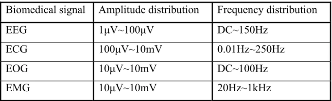
Table 1-1 The characteristics of biomedical signals
Biomedical signal Amplitude distribution Frequency distribution EEG 1μV~100μV DC~150Hz ECG 100μV~10mV 0.01Hz~250Hz EOG 10μV~10mV DC~100Hz EMG 10μV~10mV 20Hz~1kHz
Furthermore, the use of very large scale integrated circuits (VLSI) dominates medical electronics applications, which range from small, battery-powered electronic implants to room-filling diagnostic imaging systems [11]. As in other VLSI applications, the design and processing of the technology chosen for medical devices depends on the specific applications involved. Product complexity, size, sales volume, cost objectives, and available power source all play significant roles in the specific process [12]. The fabrication of VLSI may be based on the bipolar, CMOS or BiCMOS technologies. However, portable instruments and implantable products, where low power consumption is a necessity, primarily use CMOS devices. CMOS technology has become popular in the last few years for implementing complex circuits and systems. The integration of the AFE circuit and other processing units on the same chip has brought a new era in biomedical systems [13][14][15]. The cost of electronic instruments is proportional to their size, the number of devices and interconnections they contain. VLSI circuits have done a great deal to reduce size, components, and interconnections, and thus the cost of the products that contain them.
This study realized an AFE circuit design which is suitable for a portable biomedical signals recording system [2][16][17][18]. It combines the System-on-Chip (SoC) and needs no external components. It reduced the area and cost of the circuit effectively, in order to combine with DSP in the future. This study expanded the applications of the circuit. In addition, it has joined the digital controlling interface in the circuit. The user can choose the proper gain and bandwidth according to different characteristics of biomedical signals. The MSFE circuit can amplify biomedical signals to the range that can be observed and filter out the noise besides the bandwidth of biomedical signals. Consequently, the systematic structure could measure many kinds of biomedical signals.
6
1.3 Thesis Organization
The thesis is organized as follows. Chapter 2 describes the development of analog front end circuit for biomedical signal acquisition. Descriptions of MSFEIC design are in Chapter 3. Then the circuit performance and testing platform are presented in Chapter 4. Finally, a summary of this thesis research and future work is briefly concluded by Chapter 5.
7
Chapter 2
Architecture Survey
2.1 A CMOS IC for portable EEG acquisition
systems
Rui Martins et al[2]. proposed a CMOS IC for portable EEG acquisition systems in 1998.Besides low power, the key design points are high common mode rejection ratio (CMRR) and very low noise. Minimum component count is also important to reduce system weight and volume. The system includes 16 instrumentation amplifiers, one 16-to-1 analog multiplexer, a microprocessor compatible digital interface, and an internal current/voltage reference source as shown in the block diagram of Fig. 2-1.
The basic functional block diagram of current feedback amplifiers is presented in Fig. 2-2.Analyzing the input branch of this figure, we conclude that high input impedance is guaranteed by two unity gain buffers. Utilizing the current feedback, by the ratio of input impedance and output impedance to determine voltage gain, and reach high CMRR.
8
Fig. 2-2 Block diagram of an IA with current feedback [2] Design the concept as the (2-1).
ref g s out
v
v
v
R
R
v
=
⋅
(
1−
2)
+
(2-1) But it is important to note that, contrary to the classical configuration with three operational amplifiers, there is no global feedback (from the output to the input) and that there is only one high impedance node, which simplifies the frequency compensation. Another advantage is the CMRR do not depend on any matching of resistor values. The resistor count is also reduced, saving chip area.They implemented a CMOS variation of [19], as with this configuration only a reduced number of stacked transistors is necessary (improving dc behavior at low voltage power supply) and only two transistors at input are needed. Also, as PMOS transistors exhibit low flicker noise for the same area, we chose them to the input as shown in Fig. 2-3.
9
Fig. 2-3 Simplified IA circuit [2]
In order to realize high pass filter function, it was implemented using another
feedback loop around the output circuit, as shown in Fig. 2-4. The complete circuit of the IA is shown in Fig. 2-5.
10
11
2.2 A CMOS analog front-end (AFE) IC for portable
EEG/ECG monitoring applications
K. A. Ng and P. K. Chan proposed a CMOS analog front-end (AFE) IC for portable EEG/ECG monitoring applications in 2005[20]. The proposed AFE system chip is shown in Fig. 2-6. A promising approach is the differential difference amplifier (DDA) based non-inverting IA [21][22], which has favorable properties such as simplicity and acceptable low power dissipation. Fig. 2-7 shows the basic DDA non-inverting amplifier.
12
Fig. 2-7 Non-inverting DDA for use an IA [20]
The input and output relation of non-inverting DDA is defined as (2-2). The major advantage of the DDA non-inverting amplifier over the typical IA is it requires an active amplifier and two resistors to set the instrumentation gain. In this DDA-based design, the CMRR is related to the mismatch of the input ports. Mismatch between resistors R1 and
R2 only affects the gain factor, but it does not degrade the CMRR of the amplifier.
⎟⎟
⎠
⎞
⎜⎜
⎝
⎛
+
×
=
1
1 2R
R
V
V
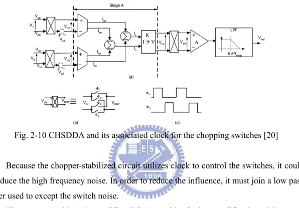
out in (2-2) Fig. 2-8 is a circuit schematic of the PMOS differential-input chopper-stabilized differential difference amplifier (CHSDDA). It joined a chopper-stabilized skill in the circuit to reduce flicker noise and DC offset voltage.13
Fig. 2-8 Circuit schematic of the PMOS CHSDDA [20]
A new rail-to-rail input IA is proposed in Fig. 2-9, which shows the filtering circuits added to the basic chopper-stabilized DDA non-inverting amplifier for suppressing this input DC offset voltage. In this realization, two CHSDDAs are arranged in parallel configuration. Input pairs are NMOS and PMOS separately, guarantee to normal running of the circuit in any input common mode voltage. In addition, the circuit added an external RC band pass filter to eliminate noise outside the frequency bandwidth of biomedical signals.
14
Fig. 2-10 shows the conceptual circuit block diagram of the chopper-stabilized DDA circuit. The two pairs of input differential voltage signals are modulated concurrently and translated to the current signals via the trans-conductance cells having identical trans-conductance gain of Gm.
Fig. 2-10 CHSDDA and its associated clock for the chopping switches [20]
Because the chopper-stabilized circuit utilizes clock to control the switches, it could produce the high frequency noise. In order to reduce the influence, it must join a low pass filter used to except the switch noise.
The programmable gain amplifier (PGA) provides further amplification with respect to the output of the rail-to-rail IA. To prevent the input impedance of the amplifier from loading the band pass filter output of the rail-to-rail IA, a non-inverting configuration is used. Note that the first chopper-stabilized stage inside the PGA is derived from the CHSDDA by just removing one input differential port. By digitally connecting the resistors via CMOS switches, the amplifier provides programmable voltage gain.
15
2.3 Low-power Low-noise 8-channel EEG front-end
ASIC for Ambulatory Acquisition Systems
Refet Firat Yazicioglu et al. proposed low-power low-noise 8-channel EEG front-end ASIC for ambulatory acquisition systems in 2006 [16]. Fig. 2-11 shows the architecture of the implemented 8-channel EEG readout front-end ASIC. Each channel of the ASIC consists of an instrumentation amplifier (IA), a spike filter (SF), a fixed gain stage, a variable gain amplifier (VGA) stage, and a channel buffer.Fig. 2-11 Architecture of the implemented 8-channel EEG front-end ASIC [16] The IA defines the noise level and CMRR of the channel, and filters the electrode offset. The second gain stage further amplifies the output of the IA and also serves as a differential to single-ended converter. The VGA is used to adjust the gain of the channels for different applications. A multiplexer, time multiplexes the output of each channel. Moreover, a bias generator and a digital control circuit generate the bias currents and digital signals for the ASIC, respectively.
Fig. 2-12 shows the implemented current feedback instrumentation amplifier (CFIA) architecture. The presented CFIA consists of only 4 main parallel branches to minimize the power dissipation, and the ratio of two resistors defines the gain (R2/R1). On the other hand, flicker noise and process related mismatches still put a limit on the minimum achievable power dissipation and CMMR. A commonly used technique to eliminate
16
flicker noise and to achieve high CMRR is called chopping [23]. However, conventional chopping amplifiers are inherently DC coupled devices. Fig. 2-12 shows the architecture of the implemented AC coupled chopped IA.
Fig. 2-12 CFIA architecture and the AC coupled chopped IA topology [16]
Fig. 2-13 shows the block diagram of the digital control circuit. It generates the necessary clock signals for the AC coupled chopped IA, the spike filter and the output multiplexer from a single clock input. Additionally, this block generates a sync-signal that can be used to synchronize the ASIC with an ADC. A non-overlapping clock generator supplies the chopping signal for the chopping switches of the AC coupled chopped IA.
17
Refet Firat Yazicioglu et al. proposed a 60 uW 60 nV/ Hz readout front-end for portable bio-potential acquisition systems in 2007 [6]. The architecture of the front-end acquisition system is shown as Fig. 2-14. The readout channel of the system consists of the AC coupled chopped instrumentation amplifier (ACCIA), a chopping spike filter (CSF) stage, a digitally programmable gain stage and an output buffer.
Fig. 2-14 Architecture of the bio-potential readout front-end for the acquisition of EEG, ECG, and EMG signals [6]
The concept of the ACCIA is shown in Fig. 2-15. DC input voltage which is the offset voltage is modulated by the input chopper and copied to the terminals of R1. The voltage
creates a current through R1 which is copied to R2 and defines the output voltage after
demodulation by the output chopper. A trans-conductance stage GM with trans-conductance and low pass cut-off frequency fp filters the DC component of the
output and converts it into current. The transfer function of the architecture is as (2-3), assuming low pass cut-off frequency of the ACCIA fLP,IA is much larger than fchop and
gmR2>>1.
)
2
(
2
)
(
2 1 2 p p in outf
gmR
s
f
s
R
R
s
V
V
π
π
+
+
=
(2-3)18
Fig. 2-15 Concept of the ACCIA [6]
On the other hand, the noise of the IA is only modulated by the output chopper. Therefore, the output noise power spectral density of ACCIA, SACCIA, can be expressed in
terms of the output noise power spectral density of the IA, SIA, as (2-4).
)
(
)
(
1
2
)
(
, 2 2f
S
nf
f
S
n
f
S
white IA odd n n chop IA ACCIA≅
−
⎟
⎠
⎞
⎜
⎝
⎛
=
∑
+∞ =−∞ =π
(2-4) If fLP,IA>>fchop and the flicker noise corner frequency of the current feedback IA is smallerthan fchop/2, SIA,white [23]. As a result, while flicker noise of the current feedback IA is
eliminated by chopping, the electrode offset is filtered by the feedback loop implemented by GM. Fig. 2-16 shows the implementation of the concept presented Fig. 2-15. This architecture can eliminate flicker noise, and external circuit reduces the offset voltage is presented by electrode and IA. The GM is implemented by the OTA2-Cext2 filter and the
trans-conductance stage, gm2. This results in an equivalent trans-conductance of Av gm2,
where Av is the voltage gain of OTA2. By replacing gm of (2-8) with Avgm2 and fp with
19
⎟⎟
⎠
⎞
⎜⎜
⎝
⎛
=
2 2 2 2 ,2
1
ext OTA ACCIA HPC
gm
gm
R
f
π
(2-5)Fig. 2-16 ACCIA implemented circuit [6]
OTA2 is implemented as a current mirror OTA as Fig. 2-17(a), where is reduced
using a series parallel division of current [24]. The gm2 stage is implemented as a basic differential stage as Fig. 2-17(b), which acts as a voltage to current converter. The combination of the two feedback loops cancels both different electrode offset (DEO) and the IA offset.
Fig. 2-17 Schematic of OTA [6]: (a) OTA1-Cext1and OTA2-Cext2 implemented circuit (b)
20
Fig. 2-18 shows the complete schematic of the implemented current feedback IA. All the current sources are implemented by paralleling the unit cascode current source, MSN1, MSN2 for NMOS current sources and MSP1, MSP2 for PMOS current sources.
Current sources I1,1 and I1,2 are implemented by combining a fixed current source and a
regulated cascade current mirror. R2 is implemented with a NMOS transistor so that the gain of the IA can be continuously adjusted. The source follower stages, which consist of transistors and act as level shifters in order to maximize the input-output voltage swing of the IA.
Fig. 2-18 Schematic of current feedback IA is used in ACCIC implementation [6] Fig. 2-19 shows the implemented chopping spike filter (CSF) stage. Before the appearance of the chopping spike, output is sampled to the capacitor and during the presence of a chopping spike, switch S is opened and output is held on the capacitor.
21
A continuous-time variable gain amplifier (VGA) stage with digitally controllable gain is shown as Fig. 2-20. Pseudo-resistors are used in order to set the DC level at the inverting node of the OTA. The VGA transfer function of the VGA is shown as (2-6).
Fig. 2-20 Schematic of the VGA [6]
⎥
⎦
⎤
⎢
⎣
⎡
+
⎟⎟
⎠
⎞
⎜⎜
⎝
⎛
⎪
⎪
⎭
⎪
⎪
⎬
⎫
⎪
⎪
⎩
⎪
⎪
⎨
⎧
⎥
⎥
⎥
⎥
⎥
⎦
⎤
⎢
⎢
⎢
⎢
⎢
⎣
⎡
⎟
⎟
⎠
⎞
⎜
⎜
⎝
⎛
+
⎟
⎟
⎠
⎞
⎜
⎜
⎝
⎛
+
+
=
1
1
1
1
)
(
1 1 1 OTA L T eq par T T vgm
C
C
C
s
R
C
s
R
C
s
C
C
s
A
(2-6)22
Chapter 3
A CMOS Mixed-Signal Front-End IC
for Portable Biopotential Acquisition
System
In this chapter, the critical issues of front-end circuit and complete mixed-signal front-end integrated circuit (MSFEIC) are presented. Section 3.1 shows the overview of MSFEIC architecture. Section 3.2 describes the critical issues of front-end circuit. Section 3.3 presents every stage of MSFEIC. The simulation results and summary are presented in Section 3.4 and 3.5, respectively.
3.1 System Architecture
This study aims to develop a bandwidth/gain tunable, low noise, low power and multi-channel mixed-signal front-end integrated circuit (MSFEIC) for patient’s biomedical signals monitoring. It amplifies the measured signals and filters other noise and makes these signals become to the meaningful information. Because the biomedical signals distribute over the very weak amplitude and very low frequency, they must be processed by MSFEIC before input the digital signal processor (DSP) to analyze. MSFEIC is divided into four parts, that including instrumentation amplifier (IA), voltage amplifier, low-pass filter (LPF), and analog-to-digital converter (ADC).
However, the measured node of the biomedical signals is not only one node, so the MSFEIC is a multi-channel design to cooperate to measure conditions practically. The structure of the MSFEIC is shown as Fig. 3-1. It is composed of four chopper-stabilized instrumentation amplifier (CHS-IA), a four-to-one analog multiplexer, a switched-capacitor variable gain amplifier (SC-VGA), a switched-capacitor low-pass
23
filter (SC-LPF), a Multi-stAge-noise-SHaping 2-1-1 tri-level sigma-delta analog-to-digital converter (MASH 2-1-1 tri-level ΣΔ ADC). In addition, MSFEIC includes a digital controlling interface with a clock generator.
Fig. 3-1 The signal flow gragh of MSFEIC
In this structure of MSFEIC, the first stage CHS-IA initially amplifies the weak biomedical signals which are received by electrodes. It defines the noise performance of the front-end. A standard IA architecture is the three-opamp IA. However, the CMRR of the three-opamp IA depends on the matching of the resistors and the need for low output impedance amplifiers results in excessive power dissipation. Thus, three-opamp IA is convenient for low-power and low-noise front-ends.
A digitally programmable gain stage with selectable gain is used to adjust the gain of the readout for different biomedical signals. Conventional gain stages use either capacitor or resistive feedback topologies, where former has consumes excessive power. In this work, a switched-capacitor topology for variable gain amplifier is applied to MSFEIC, in which input signal amplification and output load drive are separated into two different phases. This SC-VGA technique relaxes the requirement for the bandwidth and the slew rate of the operational amplifiers employed. Thus, the power consumption can be reduced.
In the last decade or so many active filters with resistors and capacitors have been replaced with a special kind of filter called a switched-capacitor filter. The switched-capacitor filter allows for very sophisticated, accurate, and tuneable analog
24
circuits to be manufactured without using resistors. This is useful for several reasons. Chief among these is that resistors are very noisy, and the circuits can be made to depend on ratios of capacitor values (which can be set accurately), and not absolute values. Moreover, it can also perform the operation of an anti-aliasing filter.
In a complete biomedical signal sensor circuit, that must includes a analog-to-digital (ADC) converter, the incorporation of an analog-to-digital converter (ADC) allows data communication with digital devices, targeted for ultimate system-on-chip approach, with the incorporation of a digital signal processor for full function.
25
3.2 Design Issues
3.2.1 Device Electronic Noise
Noise limits the minimum signal level that a circuit can process with acceptable quality. In particular, biomedical signals are very weak and susceptible to noise interference. Therefore, the input stage of biomedical signals acquisition circuit need to eliminate and popcorn noise. First of all, the need to analyze the form of noise.
Analog signals processed by integrated circuits are corrupted by two different type of noise: device electronic noise and environmental noise. We focus on device electronic noise here.
(1) Thermal Noise
Fig. 3-2 Resistor noise model
Resistance is the most common source of noise, the random motion of electrons in conductor introduces fluctuations in the voltage measured across the conductor even if the average current is zero. Thus, the spectrum of thermal noise is proportional to the absolute temperature. According to Nyquist theorem, the Effective noise power and one-sided spectral density:
26
(3-1)
(3-2)
where is the boltzmann constant. Equation (3-2) shows that noise spectral density is independent of frequency; thus, it is called “white noise”, as shown in Fig. 3-3.
Fig. 3-3 Noise one-sided spectral density
MOS transistors also exhibit thermal noise. The most significant source is the noise generated in in the channel. It can be proved that for long-channel MOS devices operating in saturation, the channel noise can be modeled by a current source connected between the drain and source terminals as shown in Fig. 3-4.
27
(2) Flicker Noise (
Noise)
Fig. 3-5 Dangling bonds at the oxide-silicon interface [25]
The interface between the gate oxide and the silicon substrate in a MOSFET entails an interesting phenomenon. Since the silicon crystal reaches an end at this interface, many “dangling” bonds appear, giving rise to extra energy states. As charge carriers move at the interface , some are randomly trapped and later released by such energy states, introducing “flicker” noise in the drain current. In addition to trapping, several other mechanisms are believed to generate flicker noise.
Unlike thermal noise, the average power of flicker noise cannot be predicted easily. Depending on the “cleanness” of the oxide-silicon interface, flicker noise may assume considerably different values and as such varies from one CMOS technology to another. The flicker noise is modeled as a voltage source in series with the gate and given by
(3-3)
where K is a process-dependent constant. As shown in Fig. 3-6, the noise spectral density is inversely proportional to the frequency.
28
Fig. 3-6 Flicker noise spectrum
From the above discussion, in order to quantify the significance of noise with respect to thermal noise for a given device, we plot both spectral densities on the same axes (Fig. 3-7), and we can reduce noise “enough” by
1. Using “large” devices and good layout. 2. Trimming (bipolar).
3. Dynamic noise-cancellation (DNC) techniques.
Fig. 3-7 Concept of noise
For this design, DNC is a good way to eliminate noise, one for the application of continuous-time, we use the chopper stabilization technique, because it has excellent long term stability, and no additional costs for testing.
29
3.2.2 Charge Injection
Charge injection occurs by channel charge when MOS switches turn off. From Fig. 3-8 we can see the channel charge flow out from the channel region of the transistor to the drain and source junctions. The channel charge of a transistor had zero drain-source voltage is given by (3-4).
(3-4)
And we derive voltage error due to charge injection is given by (3-5).
(3-5)
Switches connected to analog ground and virtual ground will cause signal -independent error because its turn-on voltage is constant. Besides these, switches connected to the signal will cause signal-dependent error which is changed with signal. Signal-dependent error is important because it truly affects resolution of the circuit. Therefore, How to reduce this kind of errors is the critical issue when we design switches of switched-capacitor circuit.
30
3.2.3 Switch Body Effect
To alleviate the body effect on a CMOS switch, we may permanently connect the body of the MOSFET to its source. However, this arrangement is not applicable to some fabrication processes. Alternatively, we use an auxiliary structure as shown in Fig. 3-9.
As the schematic shows, M3 and M4 form the main switch, while M1 and M2 forms the auxiliary switch. When clk goes low, both M1 and M3 are shut off, and the body of
M3 is tied to the highest voltage in the circuit (i.e., Vdd) through the PMOS transistor M5,
in order to prevent latch-up. When the clock signal clk goes high, both the main and auxiliary switches are conducting, and the body of the PMOS transistor M3 is connected to its source rather than to Vdd. As a result, its body-to-source voltage (Vbs) is constantly set to zero, and the body effect is thus removed. Also, its on-resistance is signifi cantly lowered [30].
31
3.2.4 Analog Nonlinearities in Cascaded Modulator
Fig. 3-10 A cascaded fourth-order (2-1-1) modulator general form with analog nonidealities.
32
Fig. 3-10 illusfrates A cascaded fourth-order (2-1-1) modulator with analog nonidealities. The DAC nonlinearities, ed1, ed2, and ed3, are represented as additive white noises, similar to the quantization error, at the corresponding feedback path of the modulator. The coefficients, γ1, γ2, and γ3, are referred to as the leakage factors of the integrators, respectively.
Ideally, the coefficients, γ1, γ2, and γ3, are all equal to unity, and the DAC errors,
ed1, ed2, and ed3, are equal to zero. In reality, mismatches in the analog components
make these coefficients vary slightiy from their ideal values, causing circuit non- linearities. Therefore, efforts need to be made to alleviate these circuit nonlinearities[26].
33
3.3 Circuit Design
The structure of MSFEIC is divided into four parts mainly (Fig. 3-11). The first stage is a chopper-stabilized instrumentation amplifier (CHS-IA), the second stage is a switched-capacitor variable gain amplifier (SC-VGA), the third stage is a switched- capacitor low-pass filter (SC-LPF), and the fourth stage is a cascaded fourth-order (2-1-1) sigma-delta analog-to digital converter (MASH 2-1-1 tri-level ΣΔ ADC). In addition, the circuit has four analog multiplexer to select signal paths and a digital control circuit to select different mode.
Fig. 3-11 The structure of MSFEIC
3.3.1 Chopper-Stabilized Instrumentation Amplifier
(CHS-IA)
34
that make them susceptible to excess noise. The chopper architecture circumvents the major issues of low power designs by using closed-loop feedback with specific timing constraints. To illustrate this concept, the proposed signal flow graph for an amplifier responding to a step is illustrated in Fig. 3-12. Feedback is a well-known technique to suppress distortion and increase precision in circuits. The implementation of feedback in this application, however, required a design paradigm. Input and feedback paths around the amplifier are conveyed as ac signals that were up-modulated to the chopper modulation frequency. The ac feedback ensures that all signals passing through the front-end of the amplifier are well above the corner for the transistors. Using ac modulation also allows for input and feedback signal chain scaling to be achieved with low-noise, on-chip capacitors as opposed to resistors that potentially draw excess power and add noise to the signal chain[27].
35
The chopper stabilization is an established technique for suppressing device electronic noises; the noises can be regarded as input refered noise, aggressor. At the input, a switch modulator translates input signal to the chopper frequency prior to entering the amplifier; and the chopper frequency must excess noise corner. After amplification, the signal is translated back to baseband, while shifting the noise up to the modulation frequency. Finally, the integrator filter out noise and retain the signal. The gain characteristics of the chopper-stabilized instrumentation amplifier are set by the input and feedback-switched capacitor networks. The amplifier summing node VA receives a differential signal input scaled by the capacitor (Fig. 3-13), and the gain we set in CHS-IA is 26 dB.
Fig. 3-13 The structure of CHS-IA
The structure of CHS-IA is shown as Fig. 3-13, the chopper modulator is composed of CMOS switch. To alleviate the body effect on a CMOS switch, we use the low body effect CMOS switch illustrated in section 3.2.3, the chopper amplifier in CHS-IA is a two stage amplifier with chopping switch[28], which is shown as Fig. 3-14.
36
Fig. 3-14 Chopper amplifier (Two stage amplifier with chopper switch)[28]
The two stage amplifier illustrated in Fig. 3-14 is based on a fully differential folded-cascode p-type two-stage Miller-compensated configuration. with active load which also allows a large output swing. Since the opamp uses a two-stage structure and a compensation capacitor, the same switching arrangement cannot be used at the output. In fact, the compensation capacitance acts like a memory element that prohibits the opamp output to be chopped instantaneously. Instead, the output of the first stage is chopped as shown in Fig. 3-14 using two sets cascode transistors M51, M52 and M61, M62. Due to the differential structure, the common-mode output voltage of both stages needs to be regulated using common-mode feedback (CMFB). In order to avoid this extra CM amplifier, the CMFB circuit for the first stage has been replaced by the cross-coupled connection of transistors M31, M32, M41, and M42. For the second stage, a simple active CMFB circuit, shown in Fig. 3-15, is used. Although the signal characteristics are purely ac at node VA(input of chopper amplifier), the amplifier must have the proper dc biasing to ensure the appropriate amplification and demodulation of the signals. Thus, the pseudoresistor is used.
37
Fig. 3-15 Active CMFB
Pre-layout simulation
(1) Chopper Amplifier
Fig. 3-16 Pre-layout simulation of chopper amplifier (Corners: TT, SS, FF, FS, SF Temperature: 0 ~100 Power supply: 1.8V±10%)
Gain > 73.4 dB PM > 62.3
38
(2) CHS-IA
Input testing signal
Input signal type:sine wave
Input signal frequency: 1.024 kHz (the max frequency that system to process) Input signal amplitude: 213 μV
Fig. 3-17 The output of CHS-IA in time-domain (Corners: TT, SS, FF, FS, SF Temperature: 0 ~100 Power supply: 1.8V±10%)
39 SPEC CHS-IA Supply Voltage 1.8 V Power Consumption 72.61 uW Gain 26 dB Nonlinearity 0.00135% Sample Rate 65.536 Hz Bandwidth 2 kHz
3.3.2 Switched-Capacitor Variable Gain Amplifier (SC-VGA)
The architecture of the switched-capacitor variable gain amplifier is shown as Fig. 3-19. SC-VGA is the second gain stage besides the CHS-IA. With the measured environment and signal amplitude at that time, SC-VGA amplifies the biomedical signals to the range easy to analyze. According to the different amplitudes of the biomedical signals, we utilized tunable digital interface to choose proper voltage gain.
40
Fig. 3-19 The structure of SC-VGA[29]
Conventional gain stage is the use of resistor topology, gain is set by parallel feedback resistor and input resistor. However, resistance configuration will consume a large amount of power and generate additional noise. Therefore, capacitor topology become a better choice, but it’s performance of power consumption is still not suitable for portable devices. In this design, we use switched-capacitor variable gain amplifier (SC-VGA)[29] to achieve signal amplification, and gain is set by parallel feedback capacitor , in which input signal amplification and output load drive are separated into two different phases. This SC-VGA technique relaxes the requirement for the bandwidth and the slew rate of the operational amplifiers employed. Thus, the power consumption can be reduced[29]. The circuit configurations of the SC-VGA in sample phase and hold phase are shown in Fig. 3-20 and Fig. 3-21, respectively.
41
Fig. 3-20 SC-VGA in sample phase
Fig. 3-21 SC-VGA in hold phase
During phase , as shown in Fig. 3-20, the first op-amp is reset and the input signal is sampled on , At the same time, the second op-amp and compensation capacitor work together as a hold circuit for previously amplified signal in phase . During phase , as shown in Fig. 3-21, the first and second with and amplify the signal sampled on previously phase [29].
42
Next, the power reduction technique will be described, the bandwidth and slew rate of the hold circuit during is given by
(3-6)
(3-7)
where is the transconductance of the second op-amp, is the current consumed in the second op-amp, and is the load capacitance. Those of the SC-VGA during shown in Fig. 3-21 are given by
(3-8)
(3-9)
where is the feedback factor, is the compensation capacitor as shown in Fig. 3-20 and Fig. 3-21, is the current consumed in the first op-amp. is the effective load capacitance in , and is assumed for simplify the analyses, also, Also, the phase margin of the two stage op-amp is assumed to be in derivation of (3-8), which is described as
(3-10)
On the other hand, if the SW1 in Fig. 3-19 is always turned on, the bandwidth and slew rate of SC-VGA in the are given by
43
(3-11)
(3-12)
and the phase margin of the two stage op-amp is assumed to be 45 in the derivation of (3-11), which is described as
(3-13)
the SC-VGA with switch1 (SW1) improve bandwidth as proportional to . When and , , which means the slew rate of the SC-VGA is limited by (3-7). The slew rate can be improved as proportional to [29]. As a result, the SC-VGA relaxes the requirement for the bandwidth and slew rate. Therefore, we use a simple structure to implement the op-amp of SC-VGA, as shown in Fig. 3-22.
44
Pre-layout simulation
(1) Input testing signal:
Input signal type: sine wave
Input signal frequency: 1.024 kHz (the max frequency that system to process) Input signal amplitude: 4.1 mV
Gain of SC-VGA: 46 dB
Fig. 3-23 The output of SC-VGA in time-domain (gain=46 dB) (Corners: TT, SS, FF, FS, SF Temperature: 0 ~100 Power supply:1.8V±10%)
45
(2) Input testing signal:
Input signal type: sine wave
Input signal frequency: 1.024 kHz (the max frequency that system to process) Input signal amplitude: 8.2 mV
Gain of SC-VGA: 40 dB
Fig. 3-25 The output of SC-VGA in time-domain (gain=40 dB) (Corners: TT, SS, FF, FS, SF Temperature: 0 ~100 Power supply: 1.8V±10%)
46
(3) Input testing signal:
Input signal type: sine wave
Input signal frequency: 1.024 kHz (the max frequency that system to process) Input signal amplitude: 16.4 mV
Gain of SC-VGA: 34 dB
Fig. 3-27 The output of SC-VGA in time-domain (gain=34 dB) (Corners: TT, SS, FF, FS, SF Temperature: 0 ~100 Power supply: 1.8V±10%)
47 SPEC SCVGA Supply Voltage 1.8 V Power Consumption 104 uW Gain 34~46 dB Nonlinearity 0.0056% Sample Rate 65.536 kHz Bandwidth 2 kHz Gain Step 6 dB
3.3.3 Switched-Capacitor Low-Pass Filter (SC-LPF)
As the most common approach for realizing accurate and linear analog signal processing (ASP) in metal-oxide semiconductor (MOS) integrated technologies, switched-capacitor (SC) circuit techniques have dominated the design of high-quality monolithic filters since the 1980s. The incomparable technological adaptability shown by SC circuits has furthermore made them the competent candidate appropriate for a rich variety of applications. In this design, switched-capacitor low-pass filter (SC-LPF) is used to realize a low-pass filter and anti-aliasing filter. The structure of SC-LPF can be divided into two kinds of high-Q and low-Q filter, and that is suitable for application of high frequency and low frequency separately. Due to the biomedical signals are all low frequency signals, so we used the low-Q biquad filter to realize the filter.The signal flow gragh of SC-LPF is shown as Fig. 3-29.
48
Fig. 3-29 The signal flow gragh of SC-LPF
The structure of SC-LPF is second-order biquad. As the graph shows, there are three forward paths and two feedback loops. Utilizing the Mason’s rule, we can obtain the transferfunction, which is given by
(3-14)
The overall dc gain of this filter (z = 1) is thus given by
(3-15)
From Fig. 3-29, we can obtain the dc signal level at node A as follows:
(3-16)
The question mark in the preceding equation stands for uncertainty, which implies that the specified transfer function H(z) cannot determine the dc signal level at node A.
49
Uncertainty essentially means flexibility, therefore a certain degree of freedom in choosing the values of , , and is obtained, and the nominal dc signal level at node A can be set at any value regardless of the three capacitance ratios[30].
Next, making use of the flexibility in choosing the values of , and , we obtain the following approximations (assuming << 1):
(3-17)
This indicates that the values of and Q can be determined by , , and . That is, , , and determine the pole positions. By contrast, it can be found that the other capacitance ratios ( , , and ) are responsible for the zero(s) only[30].
The implementation of SC-LPF is shown as Fig. 3-30, the switched-sharing is used. Although, switched-sharing can not only reduce the layout area but also save the dynamic power consumption.
50
To prevent charge injection illustrated in section 3.2.2, the circuit is controlled by two phase non-overlapping clock , and two delay phases , ; mutual matching of four clocks can effectively reduce the influences of charge injection.
Pre-layout simulation
Input testing signal:
Input signal type: sine wave
Input signal frequency: 1.024 kHz (the max frequency that system to process) Input signal amplitude: 0.82 V
Fig. 3-31 The output of SC-LPF in time-domain (Corners: TT, SS, FF, FS, SF Temperature: 0 ~100 Power supply: 1.8V±10%)
51
Fig. 3-32 The output of SC-LPF in frequency-domain (worst case)
SPEC SCLPF
Supply Voltage 1.8 V Power Consumption 124.48 uW
Gain 0 dB Nonlinearity 0.001405%
52
3.3.4 MASH 2-1-1 tri-level ΣΔ Modulator
The growing trend in biomedical signal processing is to shift more signal processing from the analog to the digital domain. This implies that the analog-to-digital converter (ADC) is moved toward the front-end system with less analog preprocessing, which makes the performance requirement more stringent.
The target performance of an ADC has at least 90-dB signal-to-noise ratio (SNR) and 100-dB spurious-free dynamic-range (SFDR) with a bandwidth exceeding 1 kHz. This design presents a 16-b 2 kHz output-rate ADC, which achieves these performance and reduces power dissipation. This ADC development involves a key design issue. That is a sigma-delta modulator (SDM) topology feasible at a low oversampling ratio (OSR) of 32. This is important for integration with the decimation filter. The resulting sampling clock of 64 kHz makes digital switching noise easier to manage, and a cost-effective single-chip solution possible. Also, a lower sampling clock will relax speed requirements in the analog circuits, and hence reduce power dissipation. In this development, an architectural approach that combines merits of cascaded SDM structures and tri-level quantization makes all quantization noise sources negligible at 32 OSR. As a result, the entire noise budget can be given to analog noise sources to reduce analog power dissipation.
Cascaded SDM structures realize high-order noise shaping by cascading sigma- delta stages of second order or lower to avoid instability, and are suited for ADCs with low OSR. A common choice is fourth-order noise shaping implemented as a 2-1-1 cascaded SDM, as shown in Fig. 3-33
53
54
In a cascaded structure, the quantization noise of the preceding stage is extracted and fed to the following stage. As a result, the digital output of the following stage includes information of quantization noise for both the preceding stage and itself. By
replicating the noise transfer function of the preceding stage in the noise cancellation logic (NCL), the quantization noise can be cancelled using the digital representation. Ideally, quantization noise of only the final stage suppressed by the total noise- shaping order appears at the SDM output, which is usually referred to as theoretical quantization noise (TQN)[31].
(3-18)
where H is the transfer function of integrator, is the quantization error of third stage. The implementation of MASH 2-1-1 tri-level ΣΔ modulator is shown as Fig. 3-34
55
ΣΔ Modulator
56
The fully differential SC increased signal dynamic range (DR), higher immunity to clock and charge feed-through, and rejection to the common-mode noise. The circuit is operated with two non-overlapping clock phases, in the phase the sampling capacitors are charged, while in the phase this charge is transferred to the integrating capacitors. In an SC system, the smallest capacitor usually generates the largest thermal noise. The size of the smallest capacitor needs to be determined according to the equation, since the thermal noise injected at the input cannot be shaped. Their sizes need to be carefully selected to prevent significant SNR loss due to the thermal noise limitation. The relationship between the modulator's SNR and its input capacitor is given by
(3-19)
where is the peak-to-peak value of the reference voltage , is the input capacitance, k is the Boltzmann's constant (1.381 ), T is the
temperatiire in Kelvin[32].
Conventionally, 1-b quantization has been used in the cascaded stages because of its inherent linearity. In this ADC, a signal-to-quantization-noise ratio (SQNR) substantially lower than the 90-dB SNR target is required. On the other hand, the use of the multibit quantizer requires dynamic element matching (DEM) algorithm to solve the nonlinear problem of multibit digital-to-analog converters (DACs). The DEM circuit usually consume considerable power and cost additional silicon area. Thus, we use the tri-level quantizer to meet the requirements. The structures of tri-level quantizer and SR-latch are shown as Fig. 3-35. Each stage use a tri-level quantizer and two SR-latch to generate the required output and feedback control signal.
57
Fig. 3-35 Tri-level quantizer and SR-latch (i=1~3)
where Vr1= , Vr0= , the output and feedback signal of each stage are constituted by the output of two SR-latch as shown in Fig. 3-36
58
To meet the required DC gain. Thus, usually a two-stage amplifier is needed. Fig. 3-37 shows the used opamp[28]. It is based on a fully differential folded-cascode p-type two-stage Miller-compensated configuration. The second stage is a common-source amplifier with active load which also allows a large output swing (-1.77 V~+1.77 V).
Fig. 3-37 Two stage operational amplifier
The performance of the modulator is greatiy influenced by the accuracy of its integrators, especially the one at the front input. The integrator's accuracy, defined by its fransient behavior, is govemed by the slew rate and unity-gain bandwidth of the amplifier. These two specifications are critical to the design of the modulator. The integrator's output is arranged to settle to its final value at half (50%) of the on-period of the clock, . The difference between the integrator's output at the half of and its ideal value is defined as the integration error, ε, which limits the maximum accuracy that the modulator can achieve[38-39].
59
Fig. 3-38 The transient behavior for the modulator[26]. The amplifier’s slew rate can be expressed as
(3-20)
where ΔV is the maximum output of integrator, is the integrator’s slewing factor in percent of , and an equation associated with the amplifier's unity-gain bandwidth and its sampling frequency can be obtained as
, (3-21)
where is the amplifier's unity-gain bandwidth in hertz, is the settling factor of the integrator in percent of , and ε is the integration error.
60
The comparator is appropriate for high-speed and low-power applications, and it operates as follows. During the reset mode (i.e., is low), the outputs are connected to VDD through M9 and M10. When goes high, the comparator enters the
regenerative mode and transistors M3–M8 form a positive feedback loop. As a result, the
input difference voltage is amplified to a full-scale rail-to-rail output. Once the comparator makes a decision, the crosscoupled transistors M3,4 and M7,8 immediately shut down all the connections between VDD and VSS, thereby saving power. This process may be better understood by looking at Fig. 3-39: When in+ is high and in- is low, out- becomes low and out+ becomes high. As a result, M3 and M8 are on, whereas M4 and M7 are off and hence the comparator is turned off[33].
VDD
VSS
61
Pre-layout simulation
Fig. 3-40 Plot of simulated SNDR versus input level Input testing signal:
Input signal type: sine wave
Input signal frequency: 1.024 kHz (the max frequency that system to process) Input signal amplitude: 0.82 V
62 SPEC ΣΔ-ADC Supply Power 1.8 V Power Consumption 271.7 uW Gain 0 dB Sample Rate 65.536 kHz Bandwidth 1.024 kHz SNDR 95.1 dB Resolution 16-bit
63
3.3.5 Digital Decimation Filter
Filtering noise which could be aliased back into the baseband is the primary purpose of the digital filtering stage. Its secondary purpose is to take the data stream that has a high sample rate and transform it into a 16-bit data stream at a lower sample rate. This process is known as decimation. Essentially, decimation is both an averaging filter function and a rate reduction function performed simultaneously. High resolution is achieved by averaging over 32 data points to interpolate between the coarse quantization levels of the modulator. The process of averaging is equivalent to lowpass filtering in the frequency domain. With the high frequency components of the quantization noise removed, the output sampling rate can be reduced to the Nyquist rate without aliasing noise into the baseband.
The simplest and most economical filter to reduce the input sampling rate is a “Comb-Filter”, because such a filter does not require a multiplier. A multiplier is not required because the filter coefficients are all unity. This comb-filter operation is equivalent to a rectangular window finite impulse response (FIR) filter. By considering the case when the down-sampling factor can be expressed as
(3-22) and the comb transfer function as
(3-23)
In this design, for M=32 and N=3, we can select
64
Using equation (3-22)~(3-23), we can modified comb filter as
(3-25)
where ki is the number of the cascaded filters Hi. ( can be removed to the
lower rate[34]). To improve the magnitude characteristic of the filter we use the cascaded cosine prefilter[35], [36] and sharpening technique[37], we can obtain
(3-26)
where (3-27) we select
(3-28)
finally, the signal flow gragh of digital decimation filter is shown as
![Fig. 2-1 IC block diagram [2]](https://thumb-ap.123doks.com/thumbv2/9libinfo/8581094.189355/21.892.232.668.767.1074/fig-ic-block-diagram.webp)
![Fig. 2-3 Simplified IA circuit [2]](https://thumb-ap.123doks.com/thumbv2/9libinfo/8581094.189355/23.892.283.608.153.441/fig-simplified-ia-circuit.webp)
![Fig. 2-6 System block diagram of the proposed AFE IC [20]](https://thumb-ap.123doks.com/thumbv2/9libinfo/8581094.189355/25.892.196.704.474.836/fig-block-diagram-proposed-afe-ic.webp)
![Fig. 2-11 Architecture of the implemented 8-channel EEG front-end ASIC [16]](https://thumb-ap.123doks.com/thumbv2/9libinfo/8581094.189355/29.892.202.729.461.685/fig-architecture-implemented-channel-eeg-end-asic.webp)
![Fig. 2-12 CFIA architecture and the AC coupled chopped IA topology [16]](https://thumb-ap.123doks.com/thumbv2/9libinfo/8581094.189355/30.892.191.723.279.676/fig-cfia-architecture-ac-coupled-chopped-ia-topology.webp)
![Fig. 2-14 Architecture of the bio-potential readout front-end for the acquisition of EEG, ECG, and EMG signals [6]](https://thumb-ap.123doks.com/thumbv2/9libinfo/8581094.189355/31.892.186.735.357.644/fig-architecture-potential-readout-acquisition-eeg-ecg-signals.webp)
![Fig. 2-16 ACCIA implemented circuit [6]](https://thumb-ap.123doks.com/thumbv2/9libinfo/8581094.189355/33.892.174.739.156.765/fig-accia-implemented-circuit.webp)
![Fig. 2-18 Schematic of current feedback IA is used in ACCIC implementation [6]](https://thumb-ap.123doks.com/thumbv2/9libinfo/8581094.189355/34.892.261.658.878.1030/fig-schematic-current-feedback-ia-used-accic-implementation.webp)
