矽鍺製程之低漏電流二極體串聯電路
及其在靜電放電防護上之應用
Design on the Low-Leakage-Current Diode
String for ESD Protection in SiGe BiCMOS
Process
研究生 : 吳偉琳
指導教授 : 柯明道 教授
Student: Woei-Lin Wu
Advisor: Prof. Ming-Dou Ker
國立交通大學
電子工程學系 電子研究所碩士班
碩 士 論 文
Submitted to Department of Electronics Engineering & Institute of Electronics College of Electrical Engineering and Computer Science
National Chiao-Tung University In Partial Fulfillment of the Requirements
for the Degree of Master
in
Electronics Engineering April 2005
Hsin-Chu, Taiwan, Republic of China
矽鍺製程之低漏電流二極體串聯電路
及其在靜電放電防護上之應用
學生: 吳 偉 琳 指導教授: 柯 明 道 教授
國立交通大學
電子工程學系 電子研究所碩士班
ABSTRACT (CHINESE)
摘要
本篇論文主旨在設計適用於矽鍺製程之靜電放電防護電路。所提出的新型電 路可以有效地降低二極體串產生的漏電流問題,且具有高的靜電放電防護能力。 本篇論文分為三大部分,透過實驗的量測以及理論的推導來驗證所提出的新型設 計。 第一部分是在0.35 微米矽鍺製程中,藉由改變元件結構以及佈局參數來探 討二極體與矽鍺異質接面雙極性電晶體之靜電放電防護能力,並利用傳輸線觸 波產生器來量測這些元件在高能量電流脈衝注入下的電壓電流特性。此外,也 探討在低壓,高壓及高速等不同應用之矽鍺異質接面雙極性電晶體,其靜電放 電防護能力。 因為寄生元件的存在,傳統的二極體串將會產生嚴重的基極漏電流問題,尤 其是在高溫的狀態下。本論文在第二部份是針對矽鍺製程中設計出新型的二極 體,並使用新型的二極體組成低漏電流二極體串聯電路。本設計配合適當的電路 技巧可有效地降低二極體串造成的漏電流問題。此外,本設計是利用二極體串在 順偏導通狀態下導去靜電放電電流,因此在小的佈局面積下就具有高的靜電放電 耐受度。 針對第二部份所提出的低漏電流二極體串聯電路作為靜電放電箝制電路,為 了達到此電路具有最低漏電流的目的,第三部分藉由推導此電路寄生元件的特性方程式以及模擬結果來達到電路設計參數的最佳化,再經由實驗的量測來驗證此 結果。本論文更進一步提出第二種新型的二極體串,從理論推導及實驗結果證明 其漏電流將更有效地被降低。此外,使用此新型二極體串作為矽鍺異質接面雙極 性電晶體之觸發電路也在本論文中被提出與驗證。 在本論文中,已經針對於矽鍺製程中設計出低漏電且高靜電放電耐受度之 二極體串聯電路,其適用於積體電路之靜電放電箝制電路。所設計的靜電放電防 護電路均已在實際晶片上成功驗證,並有數篇會議論文發表。
Design on the Low-Leakage-Current Diode
String for ESD Protection in SiGe BiCMOS
Process
Student: Woei-Lin Wu Advisor: Prof. Ming-Dou Ker
Department of Electronics Engineering & Institute of Electronics
National Chiao-Tung University
ABSTRACT (ENGLISH)
ABSTRACT
The aim in this thesis is to design the ESD protection circuits in SiGe BiCMOS process. In this design, the leakage current of the diode string can be effectively reduced and a high ESD robustness can be achieved. There are three parts in this thesis.
The first part investigates the ESD robustness of the diodes and heterojunction bipolar transistors (HBTs) by different device structures and layout parameters. The transmission line pulse generator (TLPG) is also used to investigate the characteristics of these devices under high-current stress. In addition, the ESD robustness of HBTs for low-voltage, high-voltage, and high-speed applications are also investigated.
For the traditional diode string, the parasitic p-n-p bipolar junction transistor (BJT) devices in the diode string will induce a large leakage current into the substrate, especially under high temperature condition. In the second part, a new diode structure in SiGe process is proposed and low-leakage-current diode string (LLCDS) is formed by this new diode structure. Furthermore, the leakage current of LLCDS can be
effectively reduced by extra circuit design. Because the diode string is designed to sustain the ESD stress under forward-biased condition, a high ESD robustness can be achieved in a small silicon layout area.
In the third part, the optimum design on the circuit to minimize the leakage current of LLCDS as the power-rail ESD clamp circuit is evaluated by calculating the physical formulas of the parasitic devices in the diode string and the simulation results. The experimental results are also performed to verify the simulation results. Furthermore, the second design on the diode string as the power-rail ESD clamp circuit is proposed to further reduce the leakage current. In addition, the power-rail ESD clamp circuit with new diode string as the trigger circuit of HBT is also proposed and verified.
In summary, LLCDS as the power-rail ESD clamp circuit are developed in SiGe process with low leakage current and high ESD robustness. Each of the design has been successfully verified in the testchips and also published in the international conference papers.
誌謝
ACKNOWLEDGEMENT
首先我要感謝我的指導教授柯明道博士,這一年多以來給我的指導和鼓勵。 當初剛從電子物理進到電子工程時,被教授要求做研究,常常搞不懂狀況,出錯 的次數也比較多,被教授釘的滿頭包,那時候覺得真蠻辛苦的,但是那也是我成 長最快的時候。現在回想起來,心中只有感激,而無一絲的埋怨。教授說過:「寧 願讓我們在實驗室裡被罵的臭頭,也不要在外面被別人罵。」現在我真的能夠感 同身受,體會教授的用心。 首先先感謝我的父母及兄長,有他們的栽培與鼓勵我才能站在這裡,再來感 謝實驗室的同學陳穩義與其他學長姐們對我的指導和協助,尤其是張瑋仁學長, 對剛進來的我有許多的指導與建議,讓我在實驗室能很快的適應;還有張智毅學 長,他一步步的指導我,讓我很多東西從不會到會,在短時間內能盡速的進步達 到要求,令我獲益良多。更要感謝工研院內的學長們,尤其是林昆賢學長,陳子 平學長,莊哲豪學長與陳世宏學長,讓我在工研院工讀的時期學到許許多多的待 人處世,做研究應有的態度與技巧,以及辦各種活動所需注意的事項,讓我在這 二年內的工讀生生活過的十分充實,大家在研究與生活上都給了我許多的幫忙和 建議,另外要感謝台灣積體電路公司提供取得不易的矽鍺製程,讓我能順利做研 究,在此由衷致謝。 另外我還要感謝交大桌球隊的學長姐與學弟們,尤其是在研究所時期,陪我 度過情感的低潮期,並且讓我在研究時能適當的紓解壓力,再度面對更多的挑 戰,大家的友情真的讓我很感動。 其他要感謝的人還有很多,不可勝數,在此一併謝過。 吳偉琳 九十四年四月CONTENTS
ABSTRACT (CHINESE) ... i
ABSTRACT (ENGLISH)...iii
ACKNOWLEDGEMENT ... v
CONTENTS ... vii
TABLE CAPTIONS ...viii
FIGURE CAPTIONS ... ix
Chapter 1 Introduction ... 1
1.1 MOTIVATION...1
1.2 THESIS ORGANIZATION...2
Chapter 2 Characteristics of ESD Devices in 0.35-
µm SiGe
BiCMOS Process... 4
2.1 INTRODUCTION...4
2.2 TEST STRUCTURE FOR DIODES AND HBTS ...5
2.2.1 Diodes ...5
2.2.2 HBTs...6
2.3 EXPERIMENTAL RESULTS AND DISCUSSION...7
2.3.1 Diodes ...7
2.3.2 HBTs with Different Emitter Lengths ...9
2.3.3 HBTs with Different Emitter Widths...10
2.3.4 HBTs with Different Base Resistances ... 11
2.3.5 HBTs with Different Layout Patterns ...12
2.4 CONCLUSION...13
Chapter 3 Low-Leakage-Current Diode String in 0.18-
µm
Power-Rail ESD Clamp Circuits ... 30
3.1 INTRODUCTION...30
3.2 REVIEW ON THE DIODE STRING...32
3.2.1 The Pure Diode String...32
3.2.2 The Modified Diode String to Reduce Leakage Current...32
3.3 LLCDS...33
3.4 MEASUREMENT RESULTS...34
3.5 CONCLUSION...36
Chapter 4 Minimization of Leakage Current in the Diode
String in 0.18-
µm SiGe BiCMOS Process... 45
4.1 INTRODUCTION...45
4.2 DESIGN ON POWER-RAIL ESDCLAMP CIRCUIT...47
4.2.1 Low-Leakage-Current Diode Stinrg (LLCDS) ...47
4.2.2 Low-Leakage-Current Diode String 2 (LLCDS2)...49
4.2.3 HBT Triggered by LLCDS...52
4.3 EXPERIMENTAL RESULTS...54
4.4 CONCLUSION...56
Chapter 5 Summary and Future Works ... 69
5.1 SUMMARY...69
5.2 FUTURE WORKS...70
REFERENCES ... 71
VITA 73
TABLE CAPTIONS
Table 2.1 ESD robustness of low-voltage SiGe HBT with different base nodes grounded. ...29 Table 2.2 ESD robustness of low-voltage SiGe HBT with some emitter and base
node grounded...29 Table 4.1 Parameters of devices used in the HSPICE simulation... ...68 Table 4.2 Parameters of devices measured from the experimental results...68
FIGURE CAPTIONS
Fig. 2.1 (a) Top view and (b) cross-sectional view of P-well/N-well diode in a SiGe BiCMOS process. ...14 Fig. 2.2 (a) Top view and (b) cross-sectional view of varactor (VR) diode in a SiGe
BiCMOS process. ...15 Fig. 2.3 (a) Top view and (b) cross-sectional view of vertical base-collector (VBC)
diode in a SiGe BiCMOS process...16 Fig. 2.4 The device cross-sectional view of low-voltage SiGe NPN HBT with local
collector (LC) implantation...17 Fig. 2.4 The DC characteristics of these different structure diodes...17 Fig. 2.6 Breakdown voltage versus diode type when leakage current equals to 1 µA.
...18 Fig. 2.7 Comparisons of second breakdown current among the P-well/N-well diode,
the VR diode, and the VBC+LC diode with different widths under
forward-biased condition. ...18 Fig. 2.8 Comparisons of HBM ESD robustness among the P-well/N-well diode, the
VR diode, and the VBC+LC diode with different widths under forward-biased condition. ...19 Fig. 2.9 Comparison of second breakdown current among the P-well/N-well diode,
VR diode, and VBC+LC diode with different widths under reverse-biased condition ...19 Fig. 2.10 HBM ESD robustness versus diode length of the VBC diode with the diode width of 40 µm under forward-biased condition. ...20 Fig. 2.11 Three types of ESD stress for the SiGe HBT device...20 Fig. 2.12 The TLP I-V curve of the low-voltage SiGe HBT with different emitter
lengths and a fixed emitter width of 0.45 µm under CE stress...21 Fig. 2.13 HBM ESD robustness versus emitter length of the low-voltage SiGe HBT
with emitter width of 0.45 µm. ...21 Fig. 2.14 The TLP I-V curve of the high-voltage SiGe HBT with different emitter
lengths and a fixed emitter width of 0.45 µm under CE stress...22 Fig. 2.15 HBM ESD robustness versus emitter length of the high-voltage SiGe HBT
with emitter width of 0.45 µm. ...22 Fig. 2.16 The TLP I-V curve of the high-speed SiGe HBT with different emitter
lengths and a fixed emitter width of 0.45 µm under CE stress...23 Fig. 2.17 HBM ESD robustness versus emitter length of the high-speed SiGe HBT
with emitter width of 0.45 µm. ...23 Fig. 2.18 The TLP I-V curve of the low-voltage SiGe HBT with different emitter
widths and a fixed emitter length of 30 µm under CE stress...24 Fig. 2.19 HBM ESD robustness versus emitter width of the low-voltage SiGe HBT
with emitter length of 20.3 µm. ...24 Fig. 2.20 The TLP I-V curve of the high-voltage SiGe HBT with different emitter
widths and a fixed emitter length of 30 µm under CE stress...25 Fig. 2.21 HBM ESD robustness versus emitter width of the high-voltage SiGe HBT
with emitter length of 20.3 µm. ...25 Fig. 2.22 The TLP I-V curve of the high-speed SiGe HBT with different emitter
widths and a fixed emitter length of 30 µm under CE stress...26 Fig. 2.23 HBM ESD robustness versus emitter width of the high-speed SiGe HBT
with emitter length of 20.3 µm. ...26
Fig. 2.24 The SiGe HBT with multi-finger device structure. Base resistance will increase if the base terminal is not all connected together through the contact on its top...27
Fig. 2.25 The designed high-speed implantation patterns for HBT device. K1 is the standard layout with uni-square shape. K2, K3, K4, and K5 are designed to different shapes for investigation...27
Fig. 2.26 HBM ESD robustness versus high-speed SiGe HBT with different high-speed implantation patterns. ...28
Fig. 3.1 The whole-chip ESD protection design with the diode string applied in the power-rail ESD clamp circuit. ...38
Fig. 3.2 The cross-sectional view of the pure diode string...38
Fig. 3.3 The cross-sectional view of the n-stage triple-well diode string and its parasitic base-emitter tied p-n-p bipolar transistors...39
Fig. 3.4 The top view of triple-well diode structure in 0.18-µm BiCMOS SiGe process. ...39
Fig. 3.5 The cross-sectional view of triple-well diode structure in 0.18-µm BiCMOS SiGe process...40
Fig. 3.6 The new proposed diode string with extra bias to the deep N-well to reduce the substrate leakage current...40
Fig. 3.7 The measured I-V curves along the diode string with three diodes in series (N=3) under the bias conditions (Vbias) of deep N-well floating, or biased at 1.8V. ...41
Fig. 3.8 The measured I-V curves of the different diode number of the diode string under the bias conditions (Vbias) of deep N-well floating, or biased at 1.8V, at the temperature of 25°C. ...41
Fig. 3.9 The relation between the total blocking voltage and the diode number (N) of the diode string under Vbias=1.8V at the different temperatures. ...42
Fig. 3.10 The relation between the total blocking voltage and the diode number (N) of the diode string under Vbias floating at the different temperatures. ...42
Fig. 3.11 The relation between bias resistance and total leakage current (IA + Ib) of the diode string with diode number of N=4 and bias condition of Vp=Vb=1.8V, measured at the temperatures of 25°C, 75°C, and 125°C, respectively...43
Fig. 3.12 The TLP-measured I-V curves of the diode strings with different diode numbers under the bias resistance of 10 kohm.. ...43
Fig. 3.13 The dependence of secondary breakdown current (It2) of diode string on the diode number (N) in series...44
Fig. 4.1 The whole-chip ESD protection design with the diode string applied in the power-rail ESD clamp circuit. ...58
Fig. 4.2 The cross-sectional view of the conventional diode string. ...58
Fig. 4.3 The cross-sectional view of LLCDS in 0.18-µm BiCMOS SiGe. ...59
Fig. 4.4 The equivalent circuit of LLCDS in 0.18-µm BiCMOS SiGe. ...59
Fig. 4.5 The equivalent circuit of LLCDS2 in 0.18-µm BiCMOS SiGe. ...60
Fig. 4.6 The circuit design on HBT triggered by diode for low-voltage power supply. ...60
Fig. 4.7 The equivalent circuit of LLCDS applied in another power-rail ESD clamp circuit. ...61
Fig. 4.8 The DC characteristics of the conventional diode string at 25°C. ...61
Fig. 4.9 The DC characteristics of LLCDS at 25°C. ...62
Fig. 4.11 The simulation result of the relationship between bias resistance (R) and total leakage current of LLCDS with diode number of N=4 and bias
condition of VDD=1.8V, at the temperatures of 125°C...63 Fig. 4.12 The relationship between bias resistance (R) and total leakage current of
LLCDS with diode number of N=4 and bias condition of VDD=1.8V, measured at the temperatures of 25°C, 75°C, and 125°C, respectively...63 Fig. 4.13 The simulation result of the relationship between bias resistance (R) and
total leakage current of LLCDS2 with diode number of N=4 and bias condition of VDD=1.8V, at the temperatures of 125°C...64 Fig. 4.14 The relationship between bias resistance (R) and total leakage current of
LLCDS2 with diode number of N=4 and bias condition of VDD=1.8V, measured at the temperatures of 25°C, 75°C, and 125°C, respectively...64 Fig. 4.15 The total leakage current of the conventional diode string, LLCDS and
LLCDS2 under 125°C for N=4 and R=10 kohm...65 Fig. 4.16 The dependence of secondary breakdown current (It2) of the conventional
diode string, LLCDS and LLCDS2 on the diode number (N) in series...65 Fig. 4.17 The relationship between Ro and total leakage current of the HBT triggered by conventional diode string , HBT triggered by LLCDS and HBT triggered by LLCDS2 at bias resistance (R) = 10 kohm under diode number of N=4 and bias condition of VDD=1.8V, measured at the temperatures of 125°C. ...66 Fig. 4.18 The TLP I-V curve of the HBT triggered by conventional diode string for
N=4, VDD=1.8V, and R=Ro=10 kohm. ...66 Fig. 4.19 The TLP I-V curve of the HBT triggered by LLCDS for N=4, VDD=1.8V,
and R=Ro=10 kohm...67 Fig. 4.20 The TLP I-V curve of the HBT triggered by LLCDS2 for N=4, VDD=1.8V, and R=Ro=10 kohm...67
Chapter 1
Introduction
1.1 M
OTIVATIONIn the 1990s a further revolution in bipolar transistor design occurred with the emergence of Silicon-germanium (SiGe) Heterojunction Bipolar Transistors (HBTs). Previously HBTs had only been available in compound semiconductor technologies, such as AlGaAs/GaAs. However, material research showed that a good heterojunction could be obtained if the SiGe layer was thin and the Ge content relatively low. Recently, SiGe HBT has become a key technology for RF applications in giga-bit communication systems. ESD protection in SiGe technology plays an important role in telecommunication system reliability [1]-[5].
In a SiGe BiCMOS process, with the consideration of Giga-Hz input signals, the SiGe HBT can be also used as the on-chip ESD protection device. Therefore, the relation between ESD robustness and layout parameters of SiGe HBT and diodes with different junctions should be characterized to achieve a good enough ESD protection design in such high-speed communication integrated circuits.
For ESD protection design in SiGe BiCMOS process, diode string is a good candidate as the power-rail ESD clamp circuit, because the diode string under forward-biased condition can sustain a very high ESD stress within a smaller chip area. The diode string has been widely used in integrated circuits for ESD protection [1]-[4]. However, a parasitic vertical p-n-p bipolar transistor exists in the conventional P+/N-well diode with the common P-type substrate. This parasitic vertical p-n-p bipolar transistor may cause high leakage current in the diode string [1]-[4], especially
in the high-temperature condition. To overcome the leakage problem, an extra bias to the deep N-well of the diode string with triple-well structure was proposed in this thesis. Although the additional extra bias may cause leakage current into the diode string, the overall leakage current of the diode string can be minimized by a bias resistance. Optimization design on the bias resistance was calculated and derived from the formula. The results of this design are also verified by HSPICE simulation and measured data.
1.2 T
HESISO
RGANIZATIONThe chapter 2 in the thesis discusses the structure and the device characteristics of SiGe HBTs and diodes. Five kinds of diodes including P-well/N-well diode, varactor (for voltage controlled capacitor) diode, and vertical base-collector (VBC) diode with different implantation types such as local-collector, high-speed, or without implantation are investigated. Three kinds of SiGe HBT devices are studied in this thesis, which are the low-voltage (LV) SiGe NPN HBT (BVceo = 3.8V, ft = 47GHz at Vbc = 1V), the high-voltage (HV) SiGe NPN HBT (BVceo = 6V, ft = 30GHz at Vbc = 1V), and the high-speed (HS) SiGe NPN HBT (BVceo = 2.5V, ft = 70GHz at Vbc = 1V).
In chapter 3, a new design to minimize the leakage current of the diode string is proposed. Compared with the traditional P+/N-well diode string, this structure has a deep N-well to isolate P-well and the common P-substrate. An extra bias is applied to the deep N-well to minimize the substrate leakage current. The connection of deep N-well to the extra bias makes the parasitic n-p-n of the triple-well diode being slightly turned on. This current will flow into the next diode of the diode string, but not to the common P-substrate. So, the substrate leakage current can be effectively
decreased. A resistance is further connected between the bias voltage and the deep N-well to control the leakage current level through the diode string. As the substrate leakage current could be reduced, another leakage current path appears. Because of the parasitic n-p-n bipolar transistors of the triple well diode, the leakage current will be a mount of current flow through the junction between P-well and N+ under the high-temperature condition.
In chapter 4, the leakage current and ESD robustness of Low-Leakage-Current Diode String (LLCDS) as the power clamp circuit in SiGe BiCMOS process have been investigated. By calculating the relation between bias resistance and the leakage current of LLCDS, the leakage current of LLCDS can be minimized with specified value of bias resistance. Such LLCDS can be used as the power-rail ESD clamp circuit and ESD connection cell between the separated power rails, to provide effective ESD protection in SiGe BiCMOS process.
C
HAPTER
2
Characteristics of ESD Devices in 0.35-µm SiGe
BiCMOS Process
2.1 I
NTRODUCTIONSiGe HBT has become a key technology for RF applications in giga-bit communication systems. ESD protection in SiGe technology plays an important role in telecommunication system reliability [1]-[5]. In a SiGe BiCMOS process, with the consideration of Giga-HZ input signals, the SiGe HBT is also used as the on-chip ESD protection device to protect itself.
In the 1990s a further revolution in bipolar transistor design occurred with the emergence of SiGe HBTs. Previously heterojunction bipolar transistors had only been available in compound semiconductor technologies, such as AlGaAs/GaAs. However, material research showed that a good heterojunction could be obtained if the SiGe layer was thin and the Ge content relatively low.
As the results, the relation between ESD robustness and layout parameters of SiGe HBT should be characterized to achieve a good enough ESD protection design in such high-speed communication integrated circuits. Another successful ESD protection design for RF IC applications had been reported by using the double diodes with the turn-on-efficient power-rail ESD clamp circuit [6], [7].
The relation between ESD robustness and layout parameters of diodes with different junctions in SiGe BiCMOS process should be characterized for ESD protection design. With the detailed experimental results, the on-chip ESD protection
design for Giga-Hz RF circuits can be optimized with both considerations on RF performance and ESD robustness.
In this chapter, the test structures of SiGe HBT devices and diodes with different junctions or layout parameters have been fabricated in a 0.35-µm SiGe BiCMOS process to investigate their ESD robustness.
2.2 T
ESTS
TRUCTURE FORD
IODES ANDHBT
S2.2.1 Diodes
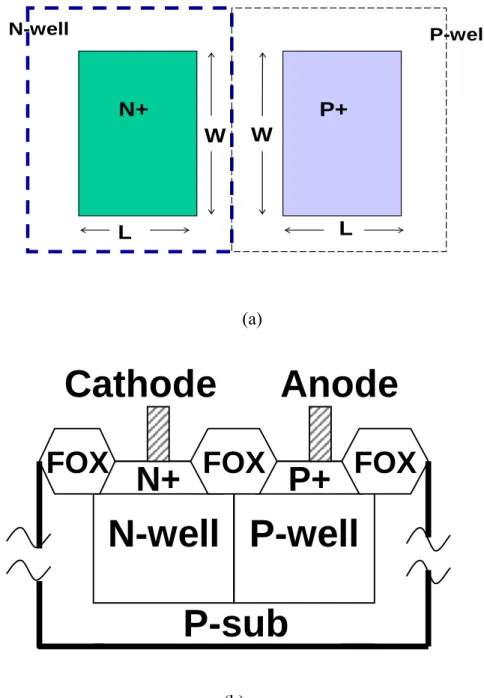
Five kinds of diodes including P-well/N-well diode, varactor (for voltage controlled capacitor) diode, and vertical base-collector (VBC) diode with different implantation types such as local-collector, high-speed, or without implantation are investigated. Fig. 2.1 shows the top view and cross-sectional view of the P-well/N-well diode, which is used as a reference for comparing with the other diodes of different structures.
Varactor means voltage controlled capacitor; is used as a diode in this research because of the junction between P+ and N-(NEPI). Fig. 2.2 shows the top view and cross-sectional view of varactor (VR) diode, where the attention will focus to the junction between P+ and N- (NEPI).
Fig. 2.3 shows the top view and cross-sectional view of VBC diode with local collector (LC) implantation. The diode junction is formed between base poly (BP) and local collector region with NEPI. In this work, next kind of diode is formed by the part of HBT for SiGe process. The emitter poly is removed and put the contact right on the base poly. As the result, the current flow through the base and collector will be
vertical. The local collector (LC) implantation under the base poly region is further changed as high-speed implantation, or even no implantation in the diode structures to compare their ESD robustness.
In the test structures for investigation, the width (W) of diode junction is drawn in the range from 3 to 12 µm, and the length (L) of diode junction is drawn from 20 to 80 µm in this work.
2.2.2 HBT Devices
The structure of the SiGe HBT device is different from the CMOS bipolar transistor. The SiGe HBT is formed by emitter poly, base poly, and N+ buried layer. Emitter poly is right on the base poly, and the base poly is right on the local collector region. The local collector region is connected with N+ buried layer and through N+ sinker to contact.
Three kinds of SiGe HBT devices are studied in this work, which are the low-voltage (LV) SiGe NPN HBT (BVceo = 3.8V, ft = 47GHz at Vbc = 1V), the high-voltage (HV) SiGe NPN HBT (BVceo = 6V, ft = 30GHz at Vbc = 1V), and the high-speed (HS) SiGe NPN HBT (BVceo = 2.5V, ft = 70GHz at Vbc = 1V). To investigate the ESD robustness of SiGe HBTs, the experimental chips had been fabricated in a 0.35-µm 3.3V/5V RF BiCMOS process.
The dependences of emitter length, emitter width, and base resistance on the ESD robustness are investigated for all LV, HV, and HS SiGe HBTs. Moreover, the pattern of high-speed implantation is also drawn with different style to investigate its impact on ESD robustness.
N-type local collector (LC) implantation region is formed under the emitter poly and connecting to the N-type sinker through the bottom N+ buried layer. The N-type sinker is formed as the collector terminal. In the high-voltage SiGe NPN HBT for 5-V operating voltage, the LC implantation is not performed for increasing the breakdown voltage of base/collector junction. On the other hand, the LC implantation is replaced by a high-speed (HS) implantation with high concentration collector region to speed up the operating speed of the HBT device.
2.3 E
XPERIMENTALR
ESULTS2.3.1 Diodes
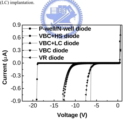
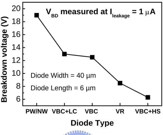
The DC characteristics of these different structure diodes are shown in Fig. 2.5. Different diode structures have different reverse breakdown voltages because of different densities of the P-N junction. Fig. 2.6 shows the breakdown voltages, defined at the current of 1 µA under reverse-biased condition, of different diode types. From the experimental result, the junction between P-well and N-well has the highest breakdown voltage.
In the varactor (VR) diode with a junction between P+ and NEPI (N), this VR diode can work with good characteristics under forward and reverse biased conditions. In the VBC diode with a junction between base poly and the local collector, it also has good characteristics under forward and reverse biased conditions. All of diodes whose leakage is less than 1nA under the normal power bias (Vdd = 3.3 V).
To observe the high current characteristics of ESD devices in SiGe BiCMOS process, transmission line pulsing (TLP) system with a pulse width of 100 ns is used
to measure the second breakdown current, It2 [8], [9]. Three diodes, the P-well/N-well diode, VR diode, and VBC+LC diode, are zapped by the TLP to find their It2. Besides TLP test, the ESD simulator is also used to measure the ESD level of devices. The ESD stress is performed with a commercial KeyTek ZapMaster ESD simulator. The start voltage of human-body-model (HBM) ESD stress is 50 V, and the step voltage is 500 V. Each measurement is performed on 2 samples, at least. Using this method, the ESD robustness of these devices can be investigated and discussed in this work.
The second breakdown current (It2) and HBM ESD robustness of the P-well/N-well diode, VR diode, and VBC+LC diode with different widths under forward-biased condition are shown in Fig. 2.7 and 2.8, respectively. The It2 and ESD robustness on the diode is increased when the diode width is increased, but that of the VBC+LC diode is not significantly improved when the diode width is further increased. Under forward-biased condition, P-well/N-well diode has the highest It2 and ESD level, which is a reference during designing the ESD protection circuit. So the P-well/N-well diode is suitable to be the ESD protection device under forward- biased condition.
Fig. 2.9 shows the second breakdown current (It2) of the P-well/N-well diode, VR diode, and VBC+LC diode with different widths under reverse-biased condition. In Fig. 2.9, the P-well/N-well diode, with a fixed length of 6 µm but different widths, has a very low second breakdown current. Although it has good ESD characteristics under forward-biased condition, it should be avoided in ESD protection design to use the P-well/N-well diode to discharge ESD current in the reverse-biased condition. For the VR diode and VBC+LC diode with a fixed length of 6 µm but different widths, their second breakdown currents are almost proportion to their widths.
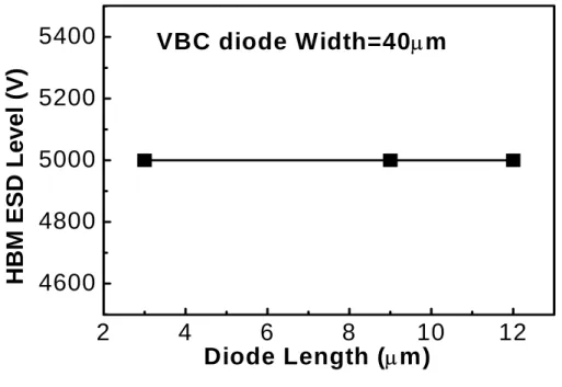
Fig. 2.10 shows the dependence of HBM ESD robustness on the diode length of the VBC diode with a fixed width of 40 µm under the forward-biased condition. In Fig. 2.10, the ESD robustness of the VBC diode is independent to the diode length. So, the VBC diode can be drawn with the minimum length for saving layout area to get the same ESD level.
2.3.2 HBT with Different Emitter Lengths
Fig. 2.11 shows three types of ESD stress for the SiGe HBT device. There are BC ESD stress, BE ESD stress and CE ESD stress. BC ESD stress is stress the base node of the SiGe HBT; collector node is grounded and emitter node is floating. BE ESD stress is stress the base node of the SiGe HBT; emitter node is grounded and collector node is floating. CE ESD stress is stress the collector node of the SiGe HBT; emitter node is grounded and base node is floating. In order to study the ESD robustness of these SiGe HBT devices completely, every kind of the junction should be tested by ESD stress.
Fig. 2.12 shows the TLP I-V curve of the low-voltage SiGe HBT with different emitter lengths and a fixed emitter width of 0.45 µm under CE stress. Fig. 2.13 shows ESD robustness of the low-voltage SiGe HBTs with a fixed emitter width of 0.45 µm but different emitter lengths. All the low-voltage SiGe HBT devices only pass 50-V HBM ESD stress when emitter width equals to 0.45 µm. Because the HBM ESD level of the CE ESD stress is too small to see the difference under different emitter lengths, the TLP I-V curve can show the more clear value.
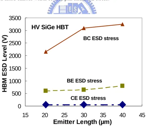
The similar results are also seen in the high-voltage SiGe HBTs with different emitter lengths, as that shown in Fig. 2.14 and Fig. 2.15. This may result from the too
small emitter width and higher junction breakdown voltage. Because the junction between base poly and local collector region has the largest area to deliver the heat under ESD stress, the HBM ESD level is highest in all ESD stress type.
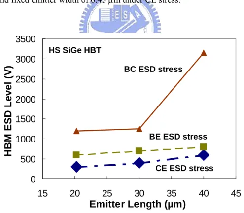
Fig. 2.16 shows the TLP I-V curve of the high-speed SiGe HBT with different emitter lengths and a fixed emitter width of 0.45 µm under CE stress. The high-speed SiGe HBTs with the lowest junction breakdown voltage have an increasing ESD robustness with the increase of emitter length, as that shown in Fig. 2.17, where the emitter width also equals to 0.45 µm.
2.3.3 HBT with Different Emitter Widths
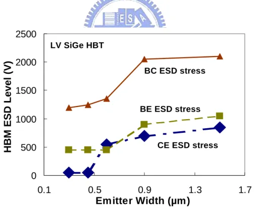
Fig. 2.18 shows the TLP I-V curve of the low-voltage SiGe HBT with different emitter width and a fixed emitter length of 30 µm under CE stress. Fig. 2.19 shows the ESD result versus the emitter width for the low-voltage SiGe HBTs under a fixed emitter length. In Fig. 2.19, the low-voltage SiGe HBT sustains higher ESD level when its emitter width is drawn larger than 0.45 µm, and achieves 800-V ESD robustness when its emitter width equals to 1.5 µm with emitter length of 20.3 µm. This equals about 20 V/µm, which is double of the ESD level of the gate-grounded NMOS in the same BiCMOS process.
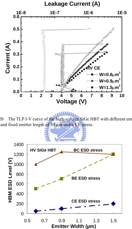
Fig. 2.20 shows the TLP I-V curve of the high-voltage SiGe HBT with different emitter width and a fixed emitter length of 30 µm under CE stress. Fig. 2.21 shows the ESD result versus the emitter width for the high-voltage SiGe HBTs under a fixed emitter length. In Fig. 2.21, the high-voltage SiGe HBT shows a relatively low ESD level. Only 200-V ESD level can be sustained, when its emitter width equals to 1.5 µm with emitter length of 20.3 µm.
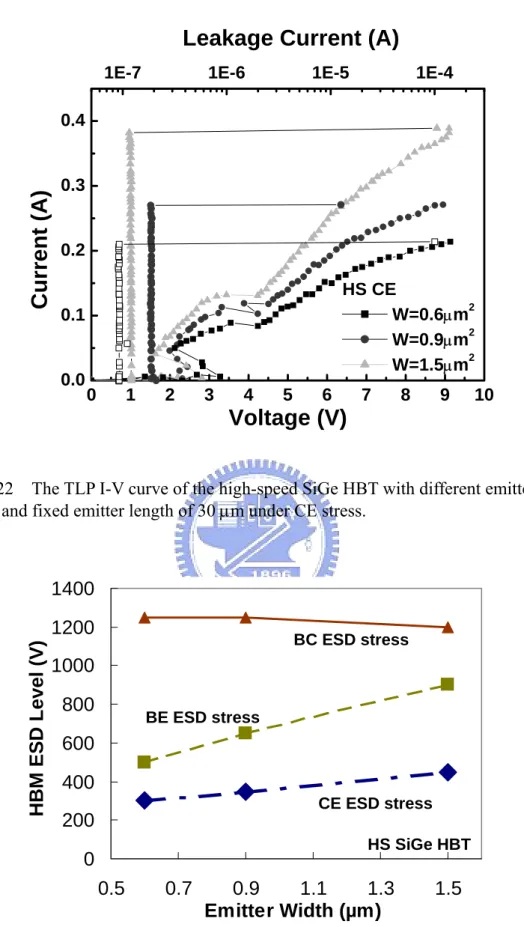
Fig. 2.22 shows the TLP I-V curve of the high-speed SiGe HBT with different emitter width and a fixed emitter length of 30 µm under CE stress. Fig. 2.23 shows the ESD result versus the emitter width for the high-voltage SiGe HBTs under a fixed emitter length. Similarly, the ESD level increases, when the emitter width of high-speed SiGe HBT increases, as shown in Fig. 2.23. If the emitter width of SiGe HBT is fixed at 0.45 µm, the order of ESD robustness is: LV SiGe HBT = HV SiGe HBT < HS SiGe HBT.
However, when the emitter width of SiGe HBT is fixed at 1.5 µm, the order of ESD robustness is: LV SiGe HBT > HS SiGe HBT > HV SiGe HBT. This is a very interesting phenomenon, and more analysis and experimental measurement will be performed in our following future work to get a clear insight.
2.3.4 HBT with Different Base Resistances
Fig. 2.24 shows the cross-sectional view of a multi-finger SiGe HBT with 4 emitter fingers. The emitter window is 20.3 µm × 0.9 µm. The base resistance can be the minimum value, when all base terminals (B1, B2, B3, B4, and B5) are connected together through the contact layer on its top.
Table I shows the ESD robustness of the low-voltage SiGe HBT when all emitter nodes are grounded, where the ESD zapping are applied to the collector node with some base nodes are grounded, such as only node1 grounded, others floating, or node 1, 3 and 5 grounded, others floating. When all base terminals are connected together to ground, only 100-V HBM ESD stress is passed. The same result also appears when the base terminals B1, B3, B5 are connected to ground.
increase to 1800 V. The floating on the base finger B5 significantly increases the ESD robustness of SiGe HBT. Table II shows the case of only one emitter and one base terminals connecting to ground. SiGe HBT with B1E2 grounded can sustain 700-V ESD stress. But, only 100-V ESD stress can be passed when B1E3 grounded. The above measured results show an interesting phenomenon, and more analysis and experimental measurement will be performed in our following work to get a clear explanation.
2.3.5 HBT with Different Layout Patterns
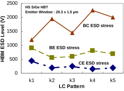
Fig. 2.25 shows the designed patterns in the high-speed SiGe HBT devices with different high-speed implantation regions. K1 is the standard layout of the high-speed SiGe HBT with unit-square shape. K2, K3, K4, and K5 are designed in different shapes for investigation. Because the SiGe HBT device is a vertical bipolar structure, the current flow may be affected by the different layout patterns of the N+ buried layer. The current flow is vertical from emitter to base, but is horizontal from N+ buried layer to N+ sinker. If the layout pattern of the N+ buried layer is discontinuously, the collector current will be harder flowing to the N+ sinker and the current distribution will not be uniform. As a result, the effect of delivering heat may be worse than other layout pattern.
Because the K4 pattern is parallel to the collector current, the current distributes uniformly, and the heat delivering may be better. As a result, The BC HBM ESD level of K4 layout pattern is the best. As for BE and CE HBM ESD level have less effect by changing N+ buried layer. The emitter window equals to 20.3 µm × 1.5 µm. The ESD robustness degrades with the designed patterns, as shown in Fig. 2.26. The standard
layout has ESD robustness about 22 V/µm, but the other patterns (K2, K3, K4, and K5) degrade to about only 50%.
2.4 C
ONCLUSIONDifferent electrostatic discharge (ESD) devices in a 0.35-µm Silicon germanium (SiGe) RF BiCMOS process are characterized in high current regime by transmission line pulse (TLP) generator and ESD simulator for on-chip ESD protection design. The test structures of diodes with different p-n junctions and the silicon-germanium heterojunction bipolar transistors (HBTs) with different layout parameters have been drawn for investigating their ESD robustness. The human-body-model (HBM) ESD robustness of SiGe HBTs with low-voltage (LV), high-voltage (HV), and high-speed (HS) implantations has been measured and compared in details.
The characteristics of diodes with different structures in the SiGe BiCMOS process have been investigated for using in ESD protection design. The diodes can work with good ESD robustness under forward-biased condition. The ESD robustness of SiGe hetrojunction bipolar transistor in the SiGe BiCMOS process has been also characterized.
If the emitter width of SiGe HBT is fixed at 0.45 µm, the order of ESD robustness is: LV SiGe HBT = HV SiGe HBT < HS SiGe HBT. However, when the emitter width of SiGe HBT is fixed at 1.5 µm, the order of ESD robustness is: LV SiGe HBT > HS SiGe HBT > HV SiGe HBT. With the proper layout parameters, SiGe HBT can perform double ESD robustness than that of NMOS device in the SiGe BiCMOS process.
P-well
W
P+
N+
N-wellL
L
W
(a)N-well P-well
P+
FOX
N+
FOX
FOX
P-sub
Cathode
Anode
(b)Fig. 2.1 (a) Top view and (b) cross-sectional view of P-well/N-well diode in a SiGe BiCMOS process.
P+
N+
N+
W
L
NEPI
DT
(a)NEPI
N
Sinker
N
Sinker
P+
FOX
FOX
N+ Buried Layer
DT
DT
Anode
Cathode
(b)Fig. 2.2 (a) Top view and (b) cross-sectional view of varactor (VR) diode in a SiGe BiCMOS process.
Base Poly
Collector
W
L
NEPI
LC
DT
(a)NEPI
Collector
Sinker
LC
FOX
N+ Buried Layer
DT
Base
Collector
DT
FOX
BP
(b)Fig. 2.3 (a) Top view and (b) cross-sectional view of vertical base-collector (VBC) diode in a SiGe BiCMOS process.
FOX FOX DT
N+ Buried Layer
LC SinkerN Base SiGe Emitter Collector EP BP DTFig. 2.4 The device cross-sectional view of low-voltage SiGe NPN HBT with local collector (LC) implantation.
-20
-15
-10
-5
0
-0.9
-0.6
-0.3
0.0
0.3
0.6
0.9
Cur
rent (
µ
A)
Voltage (V)
P-well/N-well diode
VBC+HS diode
VBC+LC diode
VBC diode
VR diode
PW/NW VBC+LC
VBC VR
VBC+HS
6
8
10
12
14
16
18
20
V
BDmeasured at I
leakage= 1
µ
A
Breakdown voltage (V)
Diode Type
Diode Width = 40 µm
Diode Length = 6 µm
Fig. 2.6 Breakdown voltage versus diode type when leakage current equals to 1 µA.
Length = 6 µm 20 30 40 50 60 70 80 0 1 2 3 4 5 6
It
2(
A
)
Diode Width (µm)
VBC+LC diode P-well/N-well diode VR diodeFig. 2.7 Comparisons of second breakdown current among the P-well/N-well diode, the VR diode, and the VBC+LC diode with different widths under forward-biased condition.
Length = 6 µm 20 30 40 50 60 70 80 2000 3000 4000 5000 6000 7000 8000
HBM ESD Le
v
e
l (
V
)
Diode Width (µm)
VBC+LC diode P-well/N-well diode VR diodeFig. 2.8 Comparisons of HBM ESD robustness among the P-well/N-well diode, the VR diode, and the VBC+LC diode with different widths under forward-biased condition.
20
30
40
50
60
70
80
0.1
0.2
0.3
0.4
0.5
0.6
0.7
It2(A)
P-well/N-well diode
VR diode
VBC+LC
Length = 6
µm
Diode Width (µm) TLPFig. 2.9 Comparison of second breakdown current among the P-well/N-well diode, VR diode, and VBC+LC diode with different widths under reverse-biased condition.
2
4
6
8
10
12
4600
4800
5000
5200
5400
HBM ESD Level (V)
Diode Length (
µm)
VBC diode Width=40
µm
Fig. 2.10 HBM ESD robustness versus diode length of the VBC diode with the diode width of 40 µm under forward-biased condition.
Fig. 2.11 Three types of ESD stress for the SiGe HBT device.
0 1 2 3 4 5 6 7 8 9 10 0.0 0.1 0.2 0.3 0.4 0.5
Current (A)
Voltage (V)
LV CE L=20µm2 L=30µm2 L=40µm21E-8 1E-7 1E-6 1E-5
Leakage Current (A)
Fig. 2.12 The TLP I-V curve of the low-voltage SiGe HBT with different emitter lengths and fixed emitter width of 0.45 µm under CE stress.
0 500 1000 1500 2000 2500 3000 3500 4000 15 20 25 30 35 40 45
Emitter Length (µm)
HBM ESD Level (V)
LV SiGe HBT BE ESD stress BC ESD stress CE ESD stressFig. 2.13 HBM ESD robustness versus emitter length of the low-voltage SiGe HBT with emitter width of 0.45 µm.
0 1 2 3 4 5 6 7 8 9 10 0.0 0.1 0.2 0.3 0.4 0.5
Current (A)
Voltage (V)
HV CE L=20µm2 L=30µm2 L=40µm21E-8 1E-7 1E-6 1E-5
Leakage Current (A)
Fig. 2.14 The TLP I-V curve of the high-voltage SiGe HBT with different emitter lengths and fixed emitter width of 0.45 µm under CE stress.
0 500 1000 1500 2000 2500 3000 3500 15 20 25 30 35 40 45
Emitter Length (µm)
HBM ESD Level (V)
HV SiGe HBT
BE ESD stress BC ESD stress CE ESD stressFig. 2.15 HBM ESD robustness versus emitter length of the high-voltage SiGe HBT with emitter width of 0.45 µm.
0 1 2 3 4 5 6 7 8 9 10 11 0.0 0.1 0.2 0.3
Current (A)
Voltage (V)
HS CE L=20µm2 L=30µm2 L=40µm21E-8 1E-7 1E-6 1E-5 1E-4 1E-3 0.01
Leakage Current (A)
Fig. 2.16 The TLP I-V curve of the high-speed SiGe HBT with different emitter lengths and fixed emitter width of 0.45 µm under CE stress.
0 500 1000 1500 2000 2500 3000 3500 15 20 25 30 35 40 45
Emitter Length (µm)
HBM ESD Level (V)
HS SiGe HBT BE ESD stress BC ESD stress CE ESD stressFig. 2.17. HBM ESD robustness versus emitter length of the high-speed SiGe HBT with emitter width of 0.45 µm.
0 1 2 3 4 5 6 7 8 9 10 11 0.0 0.1 0.2 0.3 0.4 0.5 Cur rent (A) Voltage (V) LV CE W=0.3µm2 W=0.9µm2 W=1.5µm2
1E-8 1E-7 1E-6 1E-5 1E-4 1E-3
Leakage Current (A)
Fig. 2.18 The TLP I-V curve of the low-voltage SiGe HBT with different emitter widths and fixed emitter length of 30 µm under CE stress.
0 500 1000 1500 2000 2500 0.1 0.5 0.9 1.3 1.7
Emitter Width (µm)
HBM ES
D Level (V)
LV SiGe HBT BE ESD stress BC ESD stress CE ESD stressFig. 2.19 HBM ESD robustness versus emitter width of the low-voltage SiGe HBT with emitter length of 20.3 µm.
0 1 2 3 4 5 6 7 8 9 10 0.0 0.1 0.2 0.3 0.4 0.5 0.6
Current (A)
Voltage (V)
HV CE W=0.6µm2 W=0.9µm2 W=1.5µm21E-8 1E-7 1E-6 1E-5
Leakage Current (A)
Fig. 2.20 The TLP I-V curve of the high-voltage SiGe HBT with different emitter widths and fixed emitter length of 30 µm under CE stress.
0 200 400 600 800 1000 1200 1400 0.5 0.7 0.9 1.1 1.3 1.5 Emitter Width (µm) HBM ESD Level (V) HV SiGe HBT BE ESD stress BC ESD stress CE ESD stress
Fig. 2.21 HBM ESD robustness versus emitter width of the high-voltage SiGe HBT with emitter length of 20.3 µm.
0 1 2 3 4 5 6 7 8 9 10 0.0 0.1 0.2 0.3 0.4
Current (A)
Voltage (V)
HS CE W=0.6µm2 W=0.9µm2 W=1.5µm21E-7 1E-6 1E-5 1E-4
Leakage Current (A)
Fig. 2.22 The TLP I-V curve of the high-speed SiGe HBT with different emitter widths and fixed emitter length of 30 µm under CE stress.
0 200 400 600 800 1000 1200 1400 0.5 0.7 0.9 1.1 1.3 1.5 Emitter Width (µm) HBM ESD L e vel ( V ) HS SiGe HBT BE ESD stress BC ESD stress CE ESD stress
Fig. 2.23 HBM ESD robustness versus emitter width of the high-speed SiGe HBT with emitter length of 20.3 µm.
FOX FOX FOX FOX FOX
DT DT
SiGe Base Poly
N+ Buried Layer N Sinker
C
LC LC LC LC SinkerN EPC
B1
E1
B2
E2
B3
E3
B4
E4
B5
EP EP EPFig. 2.24 The SiGe HBT with multi-finger device structure. Base resistance will increase if the base terminal is not all connected together through the contact on its top.
High Speed Implant
k2 k3 k4 k5 k1 Emitter Window
Fig. 2.25 The designed high-speed implantation patterns for HBT device. K1 is the standard layout with uni-square shape. K2, K3, K4, and K5 are designed to different shapes for investigation.
0 500 1000 1500 2000 2500 k1 k2 k3 k4 k5 LC Pattern H B M ESD L e v e l (V ) HS SiGe HBT Emitter Window : 20.3 x 1.5 µm BE ESD stress BC ESD stress CE ESD stress
Fig. 2.26 HBM ESD robustness versus high-speed SiGe HBT with different high-speed implantation patterns.
TABLE 2.1
ESD robustness of low-voltage SiGe HBT with different base nodes grounded
Gnd B12345 B135 B13 B1
HBM ESD 100 100 1800 N/A
TABLE 2.2
ESD robustness of low-voltage SiGe HBT with some emitter and base node grounded Gnd B1E1 B1E2 B1E3
Chapter 3
Low-Leakage-Current Diode String in 0.18-µm
SiGe BiCMOS Process and Its Application on
Power-Rail ESD Clamp Circuits
3.1 I
NTRODUCTIONDiode under forward-biased condition can sustain very high ESD stress within a smaller silicon area. Therefore, the diode string has been widely used in integrated circuits for ESD protection [13]-[16]. However, a parasitic vertical p-n-p bipolar transistor exists in the conventional P+/N-well diode with the common P-type substrate. This parasitic vertical p-n-p bipolar transistor often causes high leakage current in the diode string [13]-[16], especially in the high-temperature condition. Previous designs on the diode string to reduce leakage current had been reported by T. Maloney [14]-[15], which had been called as Cladded diode string, Boosted diode string, and Cantilever diode string, respectively.
But, those designs still have high leakage current at the high temperature of 125°C [17]. To significantly reduce the leakage current of the diode string in CMOS process, an NMOS-controlled lateral SCR (NCLSCR) device had been added into the diode string to result in a very low leakage level [17], even in the high-temperature condition. However, an ESD detection circuit must be designed in chip to quickly trigger the NCLSCR on.
Recently, in 0.18-µm CMOS process, the triple-well structure has been used in the diode string [18], which is expected to solve the substrate leakage current issue. The
base and emitter of the parasitic p-n-p bipolar transistor is tied together to suppress the substrate leakage current. In SiGe BiCMOS process, the deep trench (DT) was used to reduce the substrate leakage current of the diode string [19]. With the DT and n+ buried layer, the parasitic vertical p-n-p bipolar transistor in the diode string has open-base configuration, which results in a lower substrate leakage current then that of the conventional P+/N-well diode at high temperature.
Fig. 3.1 shows the typical application of the diode string in the power-rail ESD clamp circuit. Since the ESD stress may have positive or negative voltages on an input (or output) pad with respect to the grounded VDD or VSS pins. For a comprehensive ESD verification, the pin-to-pin ESD stress and the VDD-to-VSS ESD stress, had been also specified to verify the whole-chip ESD robustness. With the power-rail ESD clamp circuit, the positive-to-VSS ESD stress on the I/O pin can be discharged through the diode under forward-biased condition to VDD, and then through the power-rail ESD clamp circuit to grounded VSS [10].
So, the ESD clamp circuit between power rails is very helpful to protect I/O pin and the internal circuits of integrated circuits against ESD damage. The diode string in Fig. 3.1 is operated in forward-biased condition to discharge ESD current. Thus, it can sustain very high ESD level in a smaller silicon area. However, the main drawback for using the diode string as power-rail ESD clamp circuit is the leakage issue, especially in the high-temperature condition.
In this work, an extra bias is applied to the deep N-well of the diode string with triple-well structure to further minimize the leakage current of the diode string. The test chip has been designed, fabricated, and verified in a 0.18-µm SiGe BiCMOS process. Such diode string with minimized leakage current has been used in the power-rail ESD clamp circuit, or the ESD connection cell between the separated
power rails, to achieve whole-chip ESD protection.
3.2 R
EVIEW ON THED
IODES
TRING3.2.1 The Pure Diode String
The cross-sectional view of the pure diode string is shown in Fig. 3.2 [17]. Because of the parasitic vertical p-n-p transistor, the diode string causes more leakage current flowing into the substrate. If the gain of the parasitic vertical p-n-p transistor is above one or even larger, the addition of stacked diodes in the diode string doesn’t increase the blocking voltage across the diode string linearly.
This means that more diodes would be needed to support the same blocking voltage. To reduce the leakage current of the pure diode string, three modified designs had been reported in [17]-[18]. In order to reduce the serious substrate leakage current, there are a modified design and a new proposed design in the following section.
3.2.2 The Modified Diode String to Reduce Leakage Current
A modified design to reduce the leakage current by using triple-well technologies had been reported in [18]. Fig. 3.3 shows the cross-sectional view of the n-stage triple-well diode string with its parasitic base-emitter tied p-n-p bipolar transistors. Operating in the forward-biased condition, diode current will flow through the P-well regions, and most holes are not injected into the base region of the parasitic vertical p-n-p bipolar transistors because of the base-emitter tied configuration.
kept very small all the time before the triple-well diode string turn on. It results from the existence of the parasitic base-emitter tied p-n-p bipolar transistor.
3.3 LLCDS
In this work, low-leakage-current diode string (LLCDS) to minimize the leakage current of the diode string is proposed. The top view and cross-sectional view of the diode with deep N-well in a 0.18-µm SiGe BiCMOS process is shown in Fig. 3.4 and Fig. 3.5. Compared with the traditional P+/N-well diode string, this structure has a deep N-well to isolate P-well and the common P-substrate. An extra bias is applied to the deep N-well to minimize the substrate leakage current.
As shown in Fig. 3.6, the connection of LLCDS has a voltage applied to the deep N-well. The connection of deep N-well to the extra bias makes the parasitic n-p-n of the triple-well diode being slightly turned on. This current will flow into the next stage diode of LLCDS, but not to the common P-substrate. So, the substrate leakage current can be effectively decreased.
With the decreased substrate leakage current, total current flowing from the anode will mainly flow through the diode string itself to build up a higher blocking voltage between the power rails. Therefore, the overall leakage current through the diode string can be minimized. A resistance (Rbias) is further connected between the bias
voltage and the deep N-well to control the leakage current level through the diode string. As the substrate leakage current could be reduced, another leakage current path appears. Because of the parasitic n-p-n bipolar transistors of the triple well diode, the leakage current will be a mount of current flow through the junction between P-well and N+ under the high-temperature condition.
3.4 M
EASUREMENTR
ESULTSLLCDS, as shown in Fig. 3.6, has been fabricated in a 0.18-µm BiCMOS SiGe process. In this design, the numbers node of deep N-well in the diode string is connected out for bias, named as Vbias. The P+ anode of the diode string is marked as Vp in Fig. 3.6.
During measurement, the cathode of the diode string and the substrate are grounded with two separated channels, so that the cathode current (In) and the substrate leakage current (Isub) can be monitored separately. The total current flowing into the diode string should equal to the total current flowing out the device. The equation can be expressed as:
A b n sub
I +I = I + I (1) The measured I-V curves along the diode string with three diodes in series (N=3) under the bias conditions of deep N-well floating, or biased at 1.8V, are shown in Fig. 3.7. The diode string with Vb of 1.8V has a higher blocking voltage and a lower leakage current, as comparing to that with Vb of floating.
When IA = 1µA, the value of VDD named the total blocking voltage of the
triple-well diode string. Fig. 3.8 shows that the measured I-V curves of the different diode number of the diode string under the bias conditions (Vbias) of deep N-well floating, or biased at 1.8V, at the temperature of 25°C.
The relation between the total blocking voltage (defined at IA=1µA) and diode
number (N) of the diode string is shown in Fig. 3.9, under Vbias=1.8V to the deep N-well. In Fig. 3.9, it is apparent that the extra bias on deep N-well can increase the total blocking voltage of the diode string. The relation between the total blocking voltage (defined at IA=1µA) and diode number (N) of the diode string is shown in Fig.
3.10, under Vbias floating. Because the leakage current doesn’t flow into the substrate due to the extra bias on the deep N-well, the current is all flowing into the next stage diode in LLCDS to result in a higher blocking voltage across the diode string.
According to equation (1), when the current of Isub is far smaller then that of In, most current will flow through the diode string. As a result, applying a bias to the deep N-well will improve the blocking voltage of the triple-well diode string. But, when adding a voltage on the deep N-well, it has a leakage path from Vbias to the ground through the diode string.
So, a bias resistance (Rbias) is added to reduce the leakage current from Vb. In Fig.
3.11, the relation between bias resistance (Rbias) and the total leakage current (IA + Ib)
through the diode string with four diodes (N=4) is measured under different temperatures. The total leakage current (IA + Ib) through the diode string (N=4) under
voltage bias of Vp= Vb=1.8V is increased when the temperature is 25°C, 75°C, and 125°C.
However, this phenomenon can be further minimized by adding the bias resistance, which limits the current flow through the deep N-well (Ib). Moreover, when Ib decreases with an increasing resistance, the current flow from the anode to cathode will increase. Under this condition, the value of resistance should be optimized. From the measured results, the diode string (N=4) with a bias resistance of 10 kohm has a minimized leakage current. The equations to minimize the leakage current of the diode string with different diode stages or different blocking voltages can be further derived for optimization design.
With a bias resistance of 10 kohm, the ESD robustness of LLCDS with different diode numbers in series are investigated by the transmission-line-pulse generator (TLP) with pulse width of 100ns. As shown in Fig. 3.12, LLCDS with different diode
numbers (N) have different turn-on resistance in high-current region. The diode string with a larger diode number (n) in series has a larger turn-on resistance.
However, the secondary break-down current (It2) of LLCDS with different diode numbers (N) in series did not have obvious variation. The dependence of secondary breakdown current (It2) of LLCDS on the diode number (N) in series is shown in Fig. 3.13, where every diode has the same device dimension of W/L= 40µm/12µm in layout pattern. With an It2 of higher than 4A, LLCDS (under N=4) can sustain the human-body-model ESD stress of 6 kV. In Fig. 3.13, the It2 of the diode string will not obviously decrease when diode number increases. From this result, the number of diode in LLCDS can be reasonably increased to get a higher blocking voltage without degradation on its ESD level.
3.5 C
ONCLUSIONA new design for the diode string in 0.18-µm SiGe BiCMOS process has been proposed and verified. According to the experimental results, with extra bias to the deep N-well through a bias resistance, the total blocking voltage of the diode string can be effectively increased. Although the additional extra bias will cause some current into the diode string, the overall leakage current of the diode string can be minimized by a bias resistance.
With this new design, the substrate leakage current can be always kept in a very small value with the order of pA, even under the temperature of 125°C. This new proposed diode string is very suitable for applying in the power-rail ESD clamp circuit and the ESD connection cell between the separated power lines. Optimization design to find the best design choice on the bias resistance and its corresponding
V
DDI/O
Internal
Circuits
Power-rail ESD clamp circuit
V
SSFig. 3.1 The whole-chip ESD protection design with the diode string applied in the power-rail ESD clamp circuit.
P-substrate
P+ N+ P+ N+ P+ N+
N-well N-well N-well
VDD VSS
FOX FOX FOX FOX FOX FOX FOX FOX
P-substrate Anode Cathode FOX FOX P+ N+ P-well FOX N+ N-well Deep N-well P+ N+ P-well FOXN+ N-well Deep N-well P+ N+ P-well FOX N+ N-well Deep N-well
FOX FOX FOX
Fig. 3.3 The cross-sectional view of the n-stage triple-well diode string and its parasitic base-emitter tied p-n-p bipolar transistors.
Fig. 3.4 The top view of triple-well diode structure in 0.18-µm BiCMOS SiGe process.
Fig. 3.5 The cross-sectional view of triple-well diode structure in 0.18-µm BiCMOS SiGe process. P+ N+ N+ P-well N-well Deep N-well FOX FOX N-well
R
biasP-substrate
V
A(Anode)
GND
Ib
I
AIn
Isub
Vbias
Cathode
P+ N+ N+ P-well N-well Deep N-well FOX FOX N-well P+ N+ N+ P-well N-well Deep N-well FOX FOX N-wellFig. 3.6 The new proposed diode string with extra bias to the deep N-well to reduce the substrate leakage current.
P+ N+
N+
P-well
N-well
Deep N-well
FOX
FOX
0.0 0.5 1.0 1.5 2.0 2.5 0.0 2.0x10 -4 4.0x10 -4 6.0x10 -4 8.0x10 -4 1.0x10 -3
I
A(A
)
VDD (V)
10-14 10-12 10-10 10-8 10-6 10-4Isub
(A
)
Rbias = 10 kohm N = 3 W/L = 40/12 T = 25oC Vbias floating Vbias = 1.8 VFig. 3.7 The measured I-V curves along the diode string with three diodes in series (n=3) under the bias conditions (Vbias) of deep N-well floating, or biased at 1.8V.
0.0
0.5
1.0
1.5
2.0
2.5
0
1
2
3
Vbias =1.8V
n=2
n=3
n=4
Vbias floating
n=2
n=3
n=4
I
P(
µ
A)
VDD (V)
Fig. 3.8 The measured I-V curves of the different diode number of the diode string under the bias conditions (Vbias) of deep N-well floating, or biased at 1.8V, at the temperature of 25°C.
2
3
4
1.0
1.2
1.4
1.6
1.8
2.0
2.2
2.4
Tota l Blo cking Volta g e (V) Diode Number (N) Vbias= 1.8V T=25oC T=75oC T=125oCFig. 3.9 The relation between the total blocking voltage and the diode number (N) of the diode string under Vbias=1.8V at the different temperatures.
2
3
4
0.8
1.0
1.2
1.4
1.6
1.8
2.0
2.2
Vbais floating T=25oC T=75oC T=125oC Total B locking Voltage ( V ) Diode Number (N)Fig. 3.10 The relation between the total blocking voltage and the diode number (N) of the diode string under Vbias floating at the different temperatures.
0 500 1k 10k 20k 50k 100k 1M 1E-8 1E-7 1E-6 1E-5 1E-4 1E-3
Total Leakage Current (A)
Bias Resistance (Ohm)
T=25 oC
T=75 oC
T=125 oC
Fig. 3.11 The relation between bias resistance and total leakage current (IA + Ib) of
the diode string with diode number of n=4 and bias condition of Vp=Vb=1.8V, measured at the temperatures of 25°C ,75°C, and 125°C, respectively.
0 5 10 15 20 25 0 1 2 3 4 5
Cu
rr
e
n
t (
A)
Voltage(V)
n=1
n=2
n=3
n=4
1E-10 1E-9 1E-8 1E-7 1E-6 1E-5 1E-4 1E-3
Leakage Current (A)
Fig. 3.12 The TLP-measured I-V curves of the diode strings with different diode numbers under the bias resistance of 10 kohm.
0
1
2
3
4
3.0
3.5
4.0
4.5
5.0
It2 (A)
Diode Number (n)
Fig. 3.13 The dependence of secondary breakdown current (It2) of diode string on the diode number (n) in series.
Chapter 4
Minimization of Leakage Current in the Diode
String in 0.18-µm SiGe BiCMOS Process
4.1
I
NTRODUCTIONThe SiGe BiCMOS technology has been recognized as one of the best chip solutions for broadband and wireless systems [2]. For ESD protection design in RF circuits, the small input ESD diodes cooperating with the power-rail ESD clamp circuit can meet the circuit requirement and achieve the whole-chip ESD protection scheme[6], [20]. Fig. 4.1 shows the typical ESD protection design in RF circuits, which combines the input ESD diodes and the power-rail ESD clamp circuit. The power-rail ESD clamp circuit is implemented by the diode string [13], [14], as shown in Fig. 4.2.
ESD stress on an input (or output) pad has positive or negative modes, while the VDD or VSS pins are relatively grounded. For a comprehensive ESD verification, the pin-to- pin ESD stress and the VDD-to-VSS ESD stress, have been specified to verify the whole-chip ESD robustness. The ESD clamp circuit between the power rails is very helpful to protect the core circuits against ESD damage for RF circuit application. The ESD current can be discharged by the diode string under forward-bias condition. Therefore, the diode string can sustain a very high ESD level in a small silicon layout area. However, the main drawback for using the diode string as the power-rail ESD clamp circuit is the leakage issue, especially in the high-temperature condition. A