高壓製程之靜電放電防護元件設計
124
0
0
全文
(2) 高壓製程之靜電放電防護元件設計 HIGH-VOLTAGE ESD PROTECTION DEVICES DESIGN IN BCD PROCESS. 研 究 生:黃曄仁 指導教授:柯明道. Student: Yeh-Jen Huang Advisor: Ming-Dou Ker. 國 立 交 通 大 學 電機學院微電子奈米科技產業研發碩士班 碩 士 論 文 A Thesis Submitted to College of Electrical and Computer Engineering National Chiao Tung University in Partial Fulfillment of the Requirements for the Degree of Master In Industrial Technology R & D Master Program on Microelectronics and Nano Sciences January 2008 Hsinchu, Taiwan, Republic of China. 中華民國九十七年一月.
(3) 高壓製程之靜電放電防護元件設計 研究生:黃曄仁. 指導教授:柯明道 博士. 國立交通大學電機學院產業研發碩士班. 摘要 在高電壓(High-Voltage)靜電放電(Electrostatic Discharge, ESD)防護元 件中[如:橫向擴散金氧半功率電晶體(LDMOS Power Transistor)、金氧半 電晶體(MOSFET)、矽控整流器(SCR)、雙載子電晶體(BJT)、二極體(Diode) 和場氧化電晶體(Field Oxide Device, FOD)],BCD(Bipolar CMOS DMOS) 製程技術中的橫向擴散金氧半功率電晶體由於其可以同時作為輸出級電流 驅動(Output Current Driver)及靜電放電防護元件,故在應用面上相當廣泛, 目 前 使 用 在 薄 膜 液 晶 顯 示 器 驅 動 器 (LCD Driver) 、電源管理積體電路 (Power Management IC)和汽車電子(Motor Electronics)等領域。而金氧半電 晶體、矽控整流器、雙載子電晶體、二極體及場氧化電晶體則用作單純的 靜電放電防護元件。矽控整流器是由電流驅動而導通的元件,在高壓靜電 放電防護上由於其過高的觸發電壓(Trigger Voltage)和過低的持有電壓 (Holding Voltage),不是造成內部電路先損壞就是造成閂鎖效應(Latchup)發 生,所以要加上額外的驅動電路或是透過調變佈局參數(Layout Parameter) 去使觸發電壓降低和使持有電壓超過元件之工作電壓(Operation Voltage), 如此才可作為高壓靜電放電防護元件。 在本論文中首先會介紹各種已經被驗證的元件觸發方法去快速地將靜 -i-.
(4) 電放電能量排放及有效率地保護內部電路之氧化層,有使用當靜電放電發 生時就處於導通狀況(Initial-on)的寄生(Parasitic)元件去觸發的靜電放電防 護元件、原生性 N 型金氧半電晶體觸發矽控整流器(Native-NMOS-Triggered SCR, NANSCR)、外加的元件觸發電路、閘極耦合(Gate-Couple)、基體觸發 (Substrate-Trigger)技術、假閘極(Dummy-Gate)結構去取代原本的隔離區 (Isolation Region)之結構及透過佈局參數的改變達成元件自身基體觸發導 通(Self-Substrate-Trigger)去增加元件觸發的速度。 另外會介紹智慧功率積體電路技術(Smart Power Integrated Circuit Technology)的應用領域及各種功率電晶體[包括:V 型槽金氧半電晶體 (VMOS)、U 型槽金氧半電晶體(UMOS)、橫向擴散金氧半功率電晶體]在導 通電阻(Turn-On Resistance)上和傳統金氧半電晶體有何差異使其可應用於 輸出級電流驅動。接著介紹橫向擴散金氧半功率電晶體的元件導通機制 (Turn-On Mechanism) 和 由 於 其 特 殊 的 元 件 結 構 造 成 之 雙 重 驟 回 崩 潰 (Double-Snapback)機制。 本論文研究的第一部分是探討在 0.25μm 18V BCD 製程中各種佈局參 數下的測試元件(Testkey),其中包括高壓 N 型橫向擴散金氧半功率電晶 體、高壓 P 型橫向擴散金氧半功率電晶體、高壓 N 型場氧化電晶體、高壓 雙向矽控整流器及高壓 N 型矽控整流器(NSCR)。分別觀察其直流 I-V 特性 及傳輸線觸波脈衝(Transmission Line Pulse) I-V 特性,發現在高壓 N 型橫向 擴散金氧半功率電晶體中在調變汲極端之 N 型擴散邊緣至電接觸的距離 (N+ edge to contact spacing)由 1μm 至 4μm 時,由於其元件表面上的電阻值 提升而使電流路徑由元件表面改變成元件深處,其二次崩潰電流(Secondary Breakdown Current, It2)由原本之 0.4A 上升至 2.5A。在高壓 P 型橫向擴散金 氧半功率電晶體方面則是發現 P 型金氧半電晶體的二次崩潰電流值在大幅 調變元件的總寬度(Total Width)後只提昇了少許,在調變其他佈局參數並無 - ii -.
(5) 法使其二次崩潰電流值能夠有效提升。在高壓 N 型場氧化電晶體及高壓 N 型矽控整流器則也可以透過調變汲極端之 N 型擴散邊緣至電接觸的距離去 提升 ESD 耐受度。而在高壓雙向矽控整流器中則是發現雖然在傳輸線觸波 產生系統的量測下持有電壓可透過調變參數去超過工作電壓,但是在直流 I-V 上所觀測到的卻是只有約 2V。 本論文研究的第二部分則是介紹由製程(Process)方面去達到高壓靜電 放電防護之能力。首先說明 N 型橫向擴散金氧半功率電晶體的詳細失效機 制(Failure Mechanism)。在了解其失效機制後針對其失效點去做改善,目前 已有方法有效地使寄生於 N 型橫向擴散金氧半功率電晶體的雙載子電晶體 延緩進入導通狀態,其方法為分別在汲極端和源極端下方加入 N 型重摻雜 和 P 型重摻雜,使汲極端 N/N+接面要達成雪崩崩潰(Avalanche Breakdown) 所需的觸發電流上升及使源極端之 β gain 下降造成雙載子電晶體所需觸發 電壓上升。而在本 BCD 製程中提供了一道 P 型重摻雜的 PSB(P type Sub Body)光罩於 N 型橫向擴散金氧半功率電晶體的源極和基體端下方,去比較 在小型元件(Small Device)和大型元件(Large Device)上在加入此道光罩後對 靜電放電防護有何影響。 在小型元件上加入此道光罩可使觸發電壓及持有電壓同時上升,但卻 會有部份元件因為過大的持有電壓而使二次崩潰電流些微下降;在大型元 件上加入此道光罩可使此元件不進入驟回崩潰狀態而將不均勻導通情況改 善,同時將此元件可導通的電流達到了此元件能夠承受的最高值。. - iii -.
(6) HIGH-VOLTAGE ESD PROTECTION DEVICES DESIGN IN BCD PROCESS. Student: Yeh-Jen Huang. Advisor: Dr. Ming-Dou Ker. Industrial Technology R & D Master Program of Electrical and Computer Engineering College National Chiao Tung University. ABSTRACT The high-voltage (HV) ESD (Electrostatic Discharge, ESD) protection devices including the LDMOS power transistor, MOSFET, SCR (Silicon Controlled Rectifier), BJT (Bipolar Junction Transistor), diode and FOD (Field Oxide Device). The LDMOS in BCD (Bipolar CMOS DMOS) process can be the output current driver and ESD protection device, simultaneously. Therefore, it is applied in the fields of LCD driver, power management IC and motor electronics, etc. The MOSFET, SCR, BJT, diode and FOD are for the ESD protection device only. The SCR is a current-triggered device and it suffers the high trigger voltage and low holding voltage issues in HV ESD protection. It is necessary to add the trigger circuit and modify the layout parameter to reduce the trigger voltage and increase the holding voltage to protect the internal circuits and avoid the latchup effect. The various trigger methods to reduce the trigger voltage will be introduced first. The methods are parasitic initial-on PMOS-triggered device, native-NMOS-triggered SCR, dual-direction SCR trigger circuit, gate-couple, substrate trigger, dummy-gate structure and self-substrate-trigger. In addition, the application fields and turn-on resistance of smart power integrated circuit technology will be also introduced to discuss the reason of the VMOS, UMOS and LDMOS can be the output current driver. Then, to investigate the turn-on mechanism and the double-snapback characteristic of the LD-NMOS. - iv -.
(7) The first research of this thesis is to discuss the ESD performance of HV LD-NMOS, HV LD-PMOS, HV NFOD, HV dual-direction SCR and HV NSCR by layout modification in 0.25μm 18V BCD process. In TLP (Transmission Line Pulse) measurement, the ESD performance of LD-NMOS, NFOD and NSCR can be improved by increasing the N+ edge to contact spacing of the drain side due to the current path change. Unfortunately, the It2 (Secondary Breakdown Current) value can be improved a little by larger device total width of LD-PMOS. By layout modification, the holding voltage of dual-direction SCR can be controlled to over the operation voltage. But, the holding voltage of dual-direction SCR measured by 370A is different from the data measured by the TLP system is found. The second research of this thesis is to discuss the ESD performance of the small and large LD-NMOS devices with the PSB (P type Sub Body) layer. Due to the failure mechanism of the LD-NMOS is due to the snapback characteristic. The PSB layer is added to reduce the base resistance of the parasitic BJT and increase the trigger voltage of the LD-NMOS. Once the β gain decreased, the turn-on uniformity can be improved. The holding and trigger voltage can be both increased by the PSB layer in small LD-NMOS device; The It2 value can be increased by the PSB layer in large LD-NMOS device substantially.. -v-.
(8) ACKNOWLEDGEMENTS 回顧這兩年的碩士求學生涯,首先要感謝我的指導教授柯明道教授的細 心指導與鼓勵,使我能夠在積體電路靜電放電防護設計的領域中,由入門的 菜鳥到了解所有元件的運作機制再到能夠獨立解決問題。在做研究的態度 上,柯教授每個星期的研究群會議可以由下午五時討論到隔天早上清晨一 時,更是讓我深刻感受到教授認真的研究態度及嚴謹的處事原則。雖然在過 程中倍感艱辛,卻也獲益良多,更促使我進步及成長。 而在老師開明的指導及豐沛的研究資源下,我獲得不易取得的高壓製程 下線機會去驗證所研究的高壓 ESD 元件,也獲得老師提供充裕的研究經費使 我這兩年中不至於生活匱乏而更努力於我的研究主題。畢業之後到業界工作 更將謹記老師的名言:R & D≠Repeat & Delay 而使自己做事更有效率及水準。 在這段求學的過程中, 『奈米電子與晶片系統實驗室』是孕育我成長的母 親,在實驗室的軟硬體提供了研究的平台及學長和同學的教導及討論下使我 在學業及處世上都更精進。在此感謝張瑋仁博士、許勝福博士、陳榮昇博士、 蕭淵文、陳穩義、顏承正、陳世宏、王暢資、賴泰翔、黃俊、林群祐、莊介 堯、曾聖峰、蒙國軒、許哲綸諸位實驗室學長、同學、學弟的幫忙,更感謝 我於『世界先進積體電路股份有限公司』工讀時的主管林耿立先生、周業甯 先生及邱華琦小姐、洪嘉偉先生、吳振瑋先生和在『天鈺科技股份有限公司』 任職的前輩張智毅先生的指導於協助,使我能順利完成碩士論文。 最後,我要致上我最深的感謝給我的父親黃賽明先生、母親葉碧月女士、 祖父黃達筆先生、祖母黃德美女士及兩位姑姑黃賽月女士和黃賽青女士,感 謝他們多年來無怨的付出、照顧及鼓勵,在我困難的時候給予幫助,才能使 我勇往直前,一路走來直至今日。 黃 曄 仁 謹誌於竹塹交大 97 年 春. - vi -.
(9) CONTENTS ABSTRACT (CHINESE). i. ABSTRACT (ENGLISH). iv. ACKNOWLEDGEMENTS. vi. CONTENTS. vii. TABLE CAPTIONS. x. FIGURE CAPTIONS. xi. CHAPTER 1. INTRODUCTION. 1. 1.1. Background. 1. 1.2. The Latchup Issue in High-Voltage ESD Protection. 2. 1.2.1. The Device Structure with Latchup Immunity. 3. 1.2.2. The Latchup-Free Power-Rail ESD Clamp Circuit. 3. 1.3. The Trigger Techniques of ESD Protection Device. 4. 1.3.1. The Initial-On Parasitic Structure Technique. 5. 1.3.2. The Dual-Direction SCR with Extra Trigger Circuit. 5. 1.3.3. The Gate-Coupled Technique. 6. 1.3.4. The Substrate-Triggered Technique. 8. 1.3.5. The Native-NMOS-Triggered Technique. 9. 1.3.6. The Dummy-Gate Structure Technique. 9. 1.3.7. The Self-Substrate-Triggered Technique. 10. 1.4. Thesis Organization. 10. Figures. 12. CHAPTER 2. OVERVIEW ON POWER MOSFETs FOR HIGH-VOLTAGE ESD PROTECTION DESIGN. 2.1. Power MOS Transistors. 2.2. The Turn-On Mechanism and Double-Snapback Characteristic of. 26 26. - vii -.
(10) High-Voltage LD-NMOS and High-Voltage NMOS Devices. 29. The Isolation Technique of High-Voltage Devices. 30. 2.3 Figures. 31. CHAPTER 3. DEVICE PARAMETERS MODIFICATION FOR HIGH-VOLTAGE ESD PROTECTION DESIGN. 3.1. The High-Voltage ESD Protection Devices 3.1.1. 35 35. The High-Voltage Bipolar Junction Transistor (BJT) with Controllable Trigger and Holding Voltage. 35. 3.1.2. The High-Voltage NMOS with Embedded SCR structure (NSCR) 37. 3.1.3. The High-Voltage BJT with Embedded SCR Structure (B-SCR). 3.2. Experimental Results. 38 38. 3.2.1. The High-Voltage LD-NMOS. 38. 3.2.2. The High-Voltage LD-PMOS. 40. 3.2.3. The High-Voltage NFOD. 41. 3.2.4. The High-Voltage Dual-Direction SCR. 42. 3.2.5. The High-Voltage NSCR. 43. 3.3. Summary. 44. Tables. 45. Figures. 50. CHAPTER 4. PROCESS MODIFICATION FOR HIGH-VOLTAGE ESD PROTECTION DESIGN. 81. 4.1. The ESD Failure Mechanism of LD-NMOS. 81. 4.2. The High-Voltage BJT with ESD Implantation. 81. 4.3. The Methods to Enhance ESD Performance in LD-NMOS. 82. 4.4. 4.3.1. No Turn-On Parasitic BJT by Drain and Gate Clamp Technique. 82. 4.3.2. No-Snapback Characteristic by Adaptive Layer Technique. 83. Experimental Results and Failure Analysis 4.4.1. The Small Device with and without PSB Layer. - viii -. 84 85.
(11) 4.4.2. The Large Device with and without PSB Layer. 85. 4.4.3. The Failure Analysis of Large Device. 86. 4.5. Summary. 86. Tables. 87. Figures. 88. CHAPTER 5. CONCLUSIONS AND FUTURE WORKS. 97. 5.1. Main Results of This Thesis. 97. 5.2. Future Works. 98. Figures. 99. REFERNCES. 102. VITA. 106. - ix -.
(12) TABLE CAPTIONS CHAPTER 3 Table 3.1 Various ESD Characteristics of LD-NMOS in different device total width (W). 45 Table 3.2 Various ESD Characteristics of LD-NMOS in different OD region beyond N+ region of drain side (D_O). 45 Table 3.3 Various ESD Characteristics of LD-NMOS in different P+ edge to polygate spacing of source side (P_P). 46 Table 3.4 Various ESD Characteristics of LD-NMOS in different HV NDDD spacing (H_N) and N+ edge to contact spacing (N_C) of drain side. 46 Table 3.5 Various ESD Characteristics of LD-PMOS in different device total width (W). 47 Table 3.6 Various ESD Characteristics of LD-PMOS in different HV PDDD spacing of drain side (H_P). 48 Table 3.7 Various ESD Characteristics of LD-PMOS in different P+ edge to contact spacing of drain side (P_C). 48 Table 3.8 Various ESD Characteristics of LD-PMOS in different N+ edge to polygate spacing of source side (N_P). 49. CHAPTER 4 Table 4.1 The ESD characteristics of the small LD-NMOS device without the PSB layer. 87 Table 4.2 The ESD characteristics of the small LD-NMOS device with the PSB layer. 87. -x-.
(13) FIGURE CAPTIONS CHAPTER 1 Fig. 1.1. The I-V curve of the four common ESD protection devices: (a) gate-grounded NMOS (GGNMOS), (b) gate-VDD PMOS (GDPMOS), (c) parasitic silicon controlled rectifier (SCR), and (d) diode. 12. Fig. 1.2. The four pin-combination modes for ESD test: (a) positive-to-VSS (PS-mode), (b) negative-to-VSS (NS-mode), (c) positive-to-VDD (PD-mode), and (d) negative-to-VDD (ND-mode). 12. Fig. 1.3 Fig. 1.4. The whole-chip ESD protection circuits in CMOS IC. 13 (a) The parasitic SCR path in CMOS ICs. (b) The equivalent circuit of SCR. (c) The two terminals and four layers P-N-P-N of SCR. 13. Fig. 1.5 Fig. 1.6. The latchup-free current gain (β) product parabola curve. 14 (a) The N+/N Well guard ring, (b) The P+/P Substrate guard ring, (c) The double guard ring. 14. Fig. 1.7. The device cross-sectional views of (a) isolated HV NMOS, (b) non-isolated HV NMOS, (c) non-isolated symmetric HV NMOS, (d) isolated asymmetric HV NMOS and HV PMOS. 15. Fig. 1.8. (a) The stacked power rail ESD protection device and its RC-based detection circuit. (b) The TLP I-V curves of single FOD and stacked-FOD. 16. Fig. 1.9. (a) ~ (b) The traditional ESD protection device with the initial-off characteristic. (c) ~ (e) The ESD protection device with the initial-on characteristic. 16. Fig. 1.10 Fig. 1.11. The ESD protection design window in traditional SCR device. 17 The cross-sectional view of the initial-on SCR with PMOS trigger technique. 17. Fig. 1.12 Fig. 1.13. The equivalent circuit of the initial-on SCR with PMOS trigger. 18 The layout view of the initial-on SCR with PMOS trigger (a) The common layout pattern, (b) The n-trig node merged into the source side of the embedded PMOS structure. 18. Fig. 1.14. (a) The cross-sectional view of the dual-direction SCR structure, (b) The trigger node and the trigger method with two pair back-to-back Zener diode, (c) The TLP I-V characteristic of the dual-direction SCR. 19. Fig. 1.15. (a) The layout cell structure of the dual-direction SCR, (b) The layout view of corner cell, (c) The layout view of edge cell, (d) The layout view of center cell, (e) The cross-sectional view of corner cell, (f) The cross-sectional view of edge cell, (g) The cross-sectional view of center cell. 20. Fig. 1.16. (a) The ESD current always flow through the center-finger of GGNMOS first, (b) The center-finger will burn out by the joule heating. 21. Fig. 1.17. The gate-coupled structure and the turn-on sequence of the gate-coupled - xi -.
(14) technique.. 21. Fig. 1.18. The TLP I-V curves of various rising time of the ESD pulse.. 22. Fig. 1.19 Fig. 1.20. (a) The HV NPN BJT, (b) The HV NPN-SCR, (c) The HV NSCR. 22 The TLP I-V curves and turn-on resistances of the different substrate trigger current on GGNMOS (added trigger current:curve A > curve B > curve C). 23. Fig. 1.21. The double-substrate-triggered structure (including the P-trigger node and N-trigger node). 23. Fig. 1.22. The whole-chip ESD protection with shared ESD detection circuit for input, output and power-rail ESD clamp devices. 24. Fig. 1.23. The circuit schematics of (a) the native-NMOS-triggered SCR (NANSCR), (b) the traditional LVTSCR. 24. Fig. 1.24. The circuit schematics of (a) the native-NMOS-triggered SCR (NANSCR), (b) the traditional LVTSCR. 25. Fig. 1.25. The cross-sectional view of the self-substrate-triggered GGNMOS. The P+ trigger node connects to the source terminal of the center-finger. 25. CHAPTER 2 Fig. 2.1. Three kinds of layout patterns and its current flow path (a) The layout structure of the same side current flow, (b) The layout structure of the opposite side current flow, (b) The layout structure of the minimum metallization. 31. Fig. 2.2 Fig. 2.3. The operation region of the power transistors. 31 Four kinds cross-sectional views of power devices: (a) The VMOS device, (b) The VDMOS device, (c) The UMOS device, (d) The IGBT device. 32. Fig. 2.4 Fig. 2.5. (a) The LDMOS device, (b) The RESURF device. 32 (a) The three TLP I-V sampled points of LD-NMOS, (b) The electric field distribution versus the applied current. 33. Fig. 2.6. (a) The device structure with double snapback characteristic of HV NMOS, (b) The TLP I-V curve of device structure with double snapback characteristic of HV NMOS. 33. Fig. 2.7. (a) The device structure without double snapback characteristic of HV NMOS, (b) The TLP I-V curve of device structure without double snapback characteristic of HV NMOS. 34. Fig. 2.8. (a) The self isolation structure, (b) The junction isolation structure.. 34. CHAPTER 3 Fig. 3.1 Fig. 3.2. The HV BJT structure with controllable trigger and holding voltage. 50 The TLP I-V curves of HV BJT structure with different (a) “t” spacing, (b) “d” spacing. 50 - xii -.
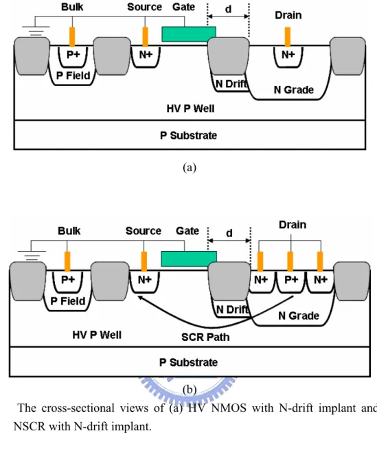
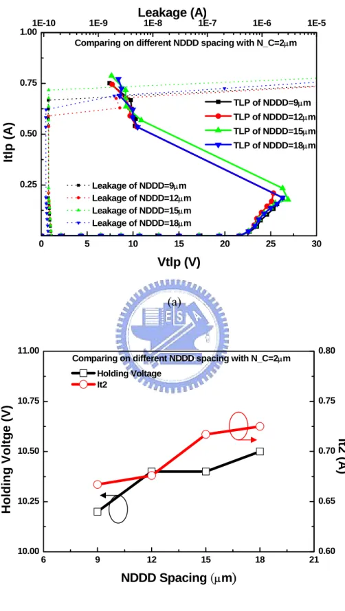
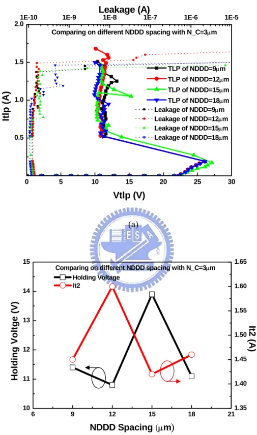
(15) Fig. 3.3. The cross-sectional views of (a) HV NMOS with N-drift implant and (b) HV NSCR with N-drift implant. 51. Fig. 3.4 Fig. 3.5. The cross-sectional view of bipolar-triggered SCR (B-SCR). 51 The TLP I-V curves of bipolar-triggered SCR (B-SCR) with different P+ spacing. 52. Fig. 3.6. (a) The cross-sectional view of LD-NMOS and the modified parameters, (b) The layout view of LD-NMOS and the modified parameters. 52. Fig. 3.7. (a) The TLP I-V curves of LD-NMOS with different total width, (b) The diagram of the holding voltage and It2 value versus the total width. 53. Fig. 3.8. (a) The TLP I-V curves of LD-NMOS with different D_O spacing, (b) The diagram of the holding voltage and It2 value versus the D_O spacing. 54. Fig. 3.9. (a) The TLP I-V curves of LD-NMOS with different P_P spacing, (b) The diagram of the holding voltage and It2 value versus the P_P spacing. 55. Fig. 3.10. (a) The TLP I-V curves of LD-NMOS with different N_C spacing, (b) The diagram of the holding voltage and It2 value versus the N_C spacing. 56. Fig. 3.11. (a) The TLP I-V curves of LD-NMOS with different H_N spacing on N_C = 1μm, (b) The diagram of the holding voltage and It2 value versus the H_N spacing. 5 7. Fig. 3.12. (a) The TLP I-V curves of LD-NMOS with different H_N spacing on N_C = 2μm, (b) The diagram of the holding voltage and It2 value versus the H_N spacing. 58. Fig. 3.13. (a) The TLP I-V curves of LD-NMOS with different H_N spacing on N_C = 3μm, (b) The diagram of the holding voltage and It2 value versus the H_N spacing. 5 9. Fig. 3.14. (a) The TLP I-V curves of LD-NMOS with different H_N spacing on N_C = 4μm, (b) The diagram of the holding voltage and It2 value versus the H_N spacing. 60. Fig. 3.15. The cross-sectional view of the LD-NMOS with separation source and bulk regions. 61. Fig. 3.16. LD-NMOS : (a) The TLP I-V curves of different total width with S_B. Fig. 3.17. spacing=0μm, (b) The TLP I-V curves of different total width with S_B spacing=2μm, (c) The It2 value versus S_B spacing on different total width. 61 LD-NMOS : (a) The TLP I-V curves of different channel length with S_B spacing=0μm, (b) The TLP I-V curves of different channel length with S_B spacing=2μm, (c) The It2 value versus S_B spacing on different channel length. 62. Fig. 3.18. LD-NMOS : (a) The TLP I-V curves of different polygate length with S_B spacing=0μm, (b) The TLP I-V curves of different polygate length with S_B spacing=2μm, (c) The It2 value versus S_B spacing on different polygate length. 63. Fig. 3.19. (a) The cross-sectional view of LD-PMOS and the modified parameters, (b) The layout view of LD-PMOS and the modified parameters. 64 - xiii -.
(16) Fig. 3.20. (a) The TLP I-V curves of LD-PMOS with different total width, (b) The diagram of the holding voltage and It2 value versus the total width. 65. Fig. 3.21. (a) The TLP I-V curves of LD-PMOS with different H_P spacing, (b) The diagram of the holding voltage and It2 value versus the H_P spacing. 66. Fig. 3.22. (a) The TLP I-V curves of LD-PMOS with different P_C spacing, (b) The diagram of the holding voltage and It2 value versus the P_C spacing. 67. Fig. 3.23. (a) The TLP I-V curves of LD-PMOS with different N_P spacing, (b) The diagram of the holding voltage and It2 value versus the N_P spacing. 68. Fig. 3.24. The cross-sectional view of NFOD and the modified parameters.. Fig. 3.25. NFOD : (a) The TLP I-V curves of different total width with S_B spacing=0μm, (b) The TLP I-V curves of different total width with S_B spacing=2μm, (c) The It2 value versus S_B spacing on different total width. 69. Fig. 3.26. NFOD : (a) The TLP I-V curves of different S spacing with S_B spacing=0μm, (b) The TLP I-V curves of different S spacing with S_B spacing=2μm, (c) The It2 value versus S_B spacing on different S spacing. 70. Fig. 3.27. NFOD : (a) The TLP I-V curves of different N_C spacing with S_B. 69. spacing=0μm, (b) The TLP I-V curves of different N_C spacing with S_B spacing=2μm, (c) The It2 value versus S_B spacing on different N_C spacing. 71 Fig. 3.28. (a) The cross-sectional view of dual-direction SCR type I and the modified parameters, (b) The layout diagram of dual-direction SCR type I. 72. Fig. 3.29. The S spacing is fixed at 2μm of dual-direction SCR type I : (a) The TLP I-V curves of different C spacing with ESD zap at node 1, (b) The TLP I-V curves of different C spacing with ESD zap at node 2, (c) The HBM and MM levels versus C spacing with ESD zap at node 1, (d) The HBM and MM levels versus C spacing with ESD zap at node 2. 72. Fig. 3.30. The S spacing is fixed at 3μm of dual-direction SCR type I : (a) The TLP I-V curves of different C spacing with ESD zap at node 1, (b) The TLP I-V curves of different C spacing with ESD zap at node 2, (c) The HBM and MM levels versus C spacing with ESD zap at node 1, (d) The HBM and MM levels versus C spacing with ESD zap at node 2. 73. Fig. 3.31. The C spacing is fixed at 3μm of dual-direction SCR type I (a) The TLP I-V curves of different S spacing with ESD zap at node 1, (b) The TLP I-V curves of different S spacing with ESD zap at node 2, (c) The HBM and MM levels versus S spacing with ESD zap at node 1, (d) The HBM and MM levels versus S spacing - xiv -.
(17) with ESD zap at node 2.. 74. Fig. 3.32. The cross-sectional view of dual-direction SCR type II and the modified parameter. 75. Fig. 3.33. Dual-direction SCR type II : (a) The TLP I-V curves of different S spacing with ESD zap at node 1, (b) The TLP I-V curves of different S spacing with ESD zap at node 2, (c) The HBM and MM levels versus S spacing with ESD zap at node 1, (d) The HBM and MM levels versus S spacing with ESD zap at node 2. 75. Fig. 3.34. The cross-sectional view of dual-direction SCR type III and the modified parameter. 76. Fig. 3.35. Dual-direction SCR type III : (a) The TLP I-V curves of different S spacing with ESD zap at node 1, (b) The TLP I-V curves of different S spacing with ESD zap at node 2, (c) The HBM and MM levels versus S spacing with ESD zap at node 1, (d) The HBM and MM levels versus S spacing with ESD zap at node 2. 76. Fig. 3.36. The cross-sectional view of NSCR and the modified parameters.. Fig. 3.37. NSCR : (a) The TLP I-V curves of different total width with S_B spacing=0μm, (b) The TLP I-V curves of different total width with S_B spacing=2μm, (c) The It2 value versus S_B spacing on different total width. 77. Fig. 3.38. NSCR : (a) The TLP I-V curves of different N_C spacing with S_B spacing=0μm, (b) The TLP I-V curves of different N_C spacing with S_B spacing=2μm, (c) The It2 value versus S_B spacing on different N_C spacing. 78. Fig. 3.39. NSCR : (a) The TLP I-V curves of different polygate length with S_B. 77. spacing=0μm, (b) The TLP I-V curves of different polygate length with S_B spacing=2μm, (c) The It2 value versus S_B spacing on different polygate length. 79 Fig. 3.40. NSCR : (a) The TLP I-V curves of different channel length with S_B spacing=0μm, (b) The TLP I-V curves of different channel length with S_B spacing=2μm, (c) The It2 value versus S_B spacing on different channel length. 80. CHAPTER 4 Fig. 4.1. (a) The cross-sectional of lateral NPN device with ESD implant, (b) Measured I-V curve for different dESD but fixed ac, with increasing the ac-dESD spacing, the current will flow through the collector diffusion and the resistance will increased. The ac-dESD spacing is curve A > curve B > curve C. 88. Fig. 4.2. (a) The I-V curve of normal operation and ESD stress by curve tracer, (b) The drain and gate clamp structure with a gate-grounded resistor. 88 - xv -.
(18) Fig. 4.3. (a) The adaptive layer structure of LD-MOS on both drain and source sides, (b) The influence on snapback effect by drain adaptive layer, (c) The influence on snapback effect by body adaptive layer. 89. Fig. 4.4 Fig. 4.5. The cross-sectional view of small LD-MOS device with the PSB layer. 89 (a) The TLP I-V curves of different S_B spacing in small LD-NMOS device without PSB layer (channel length = 15μm), (b) The TLP I-V curves of different S_B spacing in small LD-NMOS device without PSB layer (channel length =. Fig. 4.6. Fig. 4.7. 30μm). 90 (a) The TLP I-V curves of different S_B spacing in small LD-NMOS device with PSB layer (channel length = 15μm), (b) The TLP I-V curves of different S_B spacing in small LD-NMOS device with PSB layer (channel length = 30μm). 91 (a) The cross-sectional view of large LD-MOS device with the PSB layer and guarding, (b) The layout diagram of the large device. 92. Fig. 4.8. (a) The TLP I-V curves of large LD-NMOS device without PSB layer and guardring floating, (b) The TLP I-V curves of large LD-NMOS device with PSB layer and guardring floating. 93. Fig. 4.9. (a) The TLP I-V curves of large LD-NMOS device without PSB layer and guardring grounded, (b) The TLP I-V curves of large LD-NMOS device with PSB layer and guardring grounded. 94. Fig. 4.10. (a) The SEM image of large LD-NMOS device (total width = 80k μm) with PSB layer and guarding floating, (b) The SEM image of large LD-NMOS device (total width = 80k μm) with PSB layer and guarding grounded.. Fig. 4.11. 95. (a) The SEM image of large LD-NMOS device (total width = 20k μm) with PSB layer and guarding floating, (b) The SEM image of large LD-NMOS device (total width = 20k μm) with PSB layer and guarding grounded.. 96. CHAPTER 5 Fig. 5.1 Fig. 5.2 Fig. 5.3. The added trigger element to trigger the dual-direction SCR on both sides. 99 The dual-direction SCR measured by TLP and 370A. 99 (a) The TLP I-V curve of dual-direction SCR with node 1 pulse in and node 2 GND, (b) The TLP I-V curve of dual-direction SCR with node 2 pulse in and node 1 GND, (c) The DC I-V curve of dual-direction SCR with node 1 pulse in and node 2 GND, (d) The DC I-V curve of dual-direction SCR with node 2 pulse in and node 1 GND. 100. Fig. 5.4. (a) The TLP I-V curve of LD-NMOS with N_C=4μm, H_N=18 μm, (b) The DC I-V curve of LD-NMOS with N_C=4μm, H_N=18 μm, (c) The TLP I-V curve of LD-PMOS with W=400μm, (d) The DC I-V curve of LD-PMOS with W=400μm. 101 - xvi -.
(19) CHAPTER 1 INTRODUCTION. 1.1 Background Electrostatic discharge (ESD) plays a major role in the reliability issue on the semiconductor industry, which originates from the transfer of electrostatic charges between two objects with different electrical potentials and damage to integrated circuits (ICs) by large energy dissipation in an extremely short time. ESD failures become more and more serious in nanoscale CMOS processes. Common ESD failures of IC chips caused by either thermal breakdown in silicon and/or metal interconnects due to high-current transient, or dielectric breakdown in gate oxide due to high voltage overstress. The ESD specifications of commercial IC products are generally required to be higher than 2kV in human-body-model (HBM) [1] ESD stress and 200 V in machine-model (MM) ESD stress. There are several on-chip ESD protection devices that have been used for a long time, such as gate-grounded NMOS (GGNMOS), gate-VDD PMOS (GDPMOS), parasitic silicon controlled rectifier (SCR) and diode, as shown in Figs. 1.1(a) ~ 1.1(d). During normal circuit operation, these ESD protection devices are in off-state. While ESD happens, these devices will be triggered into on-state and discharge the ESD current by the low-impedance characteristic. The first point after the device snapback is named the holding point. The holding point includes two useful messages about the holding voltage and the holding current. In high-voltage (HV) ESD protection, in order to provide efficient ESD protection, the trigger voltage of the protection device should be larger than the normal circuit operation voltage and smaller than the internal circuit’s gate oxide breakdown voltage [2]-[3]. The on-chip ESD protection circuits have to be added between the input/output (I/O) pad and VDD/VSS to provide the desired ESD robustness in CMOS ICs [4]-[5]. There are four pin-combination modes on an I/O pad while ESD stressing: positive-to-VSS (PS-mode), negative-to-VSS (NS-mode), positive-to-VDD (PD-mode), and negative-to-VDD (ND-mode), as shown in Figs. 1.2(a) ~ 1.2(d), respectively. For example, the PS-mode means a positive stress at the I/O pad to discharge through the grounded VSS, while the VDD and other pins are floating. The locations of the ESD -1-.
(20) protection circuits to achieve whole-chip ESD protection for CMOS ICs are illustrated in Fig. 1.3. To avoid the unexpected ESD damage in the internal circuits of CMOS ICs, the turn-on-efficient power-rail ESD clamp circuit was placed between VDD and VSS power lines [6]. ESD current at the I/O pad under the PS-mode ESD stress can be discharged through the parasitic diode of PMOS from I/O pad to VDD, and then through the VDD-to-VSS ESD clamp circuit to ground.. 1.2 The Latchup Issue in High-Voltage ESD Protection With the special application in HV operation, latchup [7]-[8] is more serious than in low-voltage operation. In HV operation, the holding voltage is always smaller than the operation voltage, the parasitic SCR in CMOS technology will be triggered and cannot be off. The reason is the positive feedback generated by the large enough substrate or well current as shown in Figs. 1.4(a) ~ 1.4(c). The parasitic circuit includes two BJTs (one is NPN, the other is PNP) and two resistors. The SCR is a two-terminals and four-layers PNPN (P+/N Sub/P Well/N+) structure. The trigger voltage is determined by the avalanche breakdown voltage of N Sub/P Well junction. When a positive voltage applied on the anode of SCR is larger than the breakdown voltage and its cathode is relatively grounded. Through the avalanche breakdown, the generation of hole and electron is launched. If the voltage drop across the resistor is larger than 0.7 V, the parasitic BJT will be turn on and initiates the SCR into latching state. Once the SCR is triggered on, the required holding current to keep the NPN and PNP transistors on is no longer involving the avalanche breakdown mechanism. Due to this reason, the holding voltage of SCR is always at low voltage level around 5 V. However, if the resistor is large enough, the latchup happens more easily. Once latchup happens, the current will conduct through a low-impedance path from the power supply to ground. If the current is not limited, irreversible damage will happen by the latchup-generated high power. Even though the current is limited, the CMOS ICs may be malfunction. In order to avoid the latchup effect, there are several methods that have be developed, such as well-designed SCR structure, epitaxial layer, silicon on insulator (SOI), trench isolation and layout parameter with modified anode-to-cathode spacing, guard ring width. The well-designed SCR structure means the SCR is latchup-free by itself through the product of the βnpn and βpnp is smaller than 1, as shown in Fig. 1.5. The guard ring types are shown in Fig. 1.6, including the single guard ring and the double guard ring. -2-.
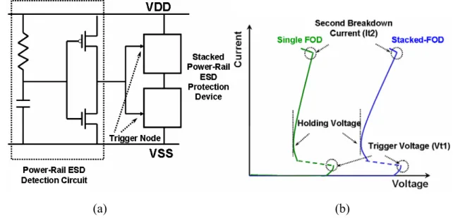
(21) 1.2.1. The Device Structures with Latchup Immunity. The HV ESD protection device with sufficient latchup immunity is necessary. The device with isolated and asymmetric structure has been verified that has the better latchup immunity than the non-isolated and symmetry structure. The isolated structure means that there is an additional N+ burier layer (NBL) beneath the N Well or P Well combine with its peripheral N Well regions and the non-isolated structure is without the NBL layer [9], as shown in Figs. 1.7(a) and 1.7(b), respectively. The isolated structure can prevent the possible leakage current path between outside and inside device. The asymmetric structure means that not both the drain and source sides enclosed with N Well region. The N Well region is a lightly doped layer and it is used to sustain high breakdown voltage. On the other hand, the symmetry structure means both the drain and source sides can sustain high voltage as shown in Fig. 1.7(c), but the turn-on resistance is large than asymmetric structure. To investigate the latchup characteristic in HV CMOS process, the transmission line pulsing (TLP) generator is used to measure the latchup I-V curves. The TLP system was invented by T. J. Maloney and N. Khurana (Intel) in 1985, it generates a short width (rise time) of 100ns (10ns) and high current square pulse [10]. Since then, TLP has allowed tremendous insight into the electrical characteristics of ESD protection circuits and devices. The main value of TLP is to reduce the design cycle time for the ESD protection circuits. The TLP system is to simulate the real ESD current discharge event and it’s the most accurate facility to measure the trigger voltage, holding voltage and secondary breakdown current (It2) of the device under test (DUT). On the other hand, the TLP will not damage the HV devices so easier than continuous-type curve tracer Tektronix 370A due to its shorter pulse width and limited energy [11]. Compared with the non-isolated and symmetry structure, the device with isolated and asymmetric structure has better latchup immunity due to its higher trigger and holding voltage, as shown in Fig. 1.7(d). By the way, to raise the layout parameter of anode-to-cathode spacing will improve the latchup immunity due to the holding voltage increasing by the increased SCR current path. However, increasing guard ring width only has a little improvement on latchup immunity of isolated structure, because the dominant factor is the isolation region of NBL/P well junction, not the guard ring structure.. 1.2.2. The Latchup-Free Power-Rail ESD Clamp Circuit. -3-.
(22) While using the HV ESD protection device on the power-rail ESD clamp, the holding voltage must be smaller than the power supply voltage, the ESD device may be triggered on by the system-level electromagnetic compatibility (EMC)/ESD transient pulses to cause a very serious latchup or latchup-like failure in CMOS ICs [12]. The increasing of the holding voltage method is developed by the stacked device technique. On the stacked Field Oxide Device (FOD), the total trigger voltage and holding voltage are the sum of the single device. For example, if the trigger voltage and holding voltage of single device are 30 V and 15 V. With two stacked devices, the total trigger voltage and holding voltage are 60 V and 30 V. Through this technique, the holding voltage is doubled, but the drawback is that the trigger voltage is also doubled, as shown in Figs. 1.8(a) and 1.8(b). In order to get a turn-on-efficient power-rail ESD clamp, the extra ESD detection circuit is added to detect the ESD pulse on the power line and let the trigger voltage be smaller. The power-rail ESD detection circuit is composed of a resistor, a capacitor and an inverter. This detection circuit is also called RC-inverter. Due to the ESD pulse happens on nanosecond order duration. The product of the resistor and capacitor is always set to microsecond order to distinguish the normal circuit operation and the ESD stress event. The inverter is used to push the NMOS in the next stage. To match the value of the resistor and capacitor is another issue. Although the product of the resistor and capacitor is the same, it may cause the turn-on efficiency something different. Moreover, another drawback of the stacked technique is the turn-on resistance is also increased, because the connection of the stacked devices is in series type.. 1.3 The Trigger Techniques of ESD Protection Device Because of the total power dissipation of one certain device is fixed at the product of the It2 and holding voltage (power = It2 x Vhold ), the SCR device can sustain a much higher It2 than other devices in a smaller layout due to its low holding voltage characteristic. So, it had been used to protect the internal circuits against ESD damage for a long time. But, the trigger voltage of the HV SCR is too large to protect the internal circuit. Therefore, how to decrease the trigger voltage in HV operation is another issue. There are several SCR-based structure had been verified. The application method is to integrate two kinds of devices into one device by using the low holding voltage characteristic of SCR and the low trigger voltage of other devices. The integration method can be one device with parasitic SCR path or SCR device with parasitic trigger device. -4-.
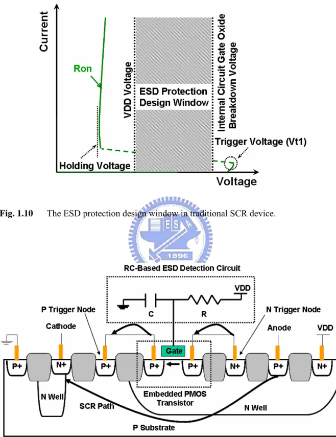
(23) 1.3.1. The Initial-On Parasitic Structure Technique. In the past, the traditional ESD protection devices are use the parasitic BJT to turn on the GGNMOS and use the avalanche breakdown to turn on the SCR. But, with the device scaling, the internal circuits are fabricated on thinner oxide, the traditional ESD protection design cannot be able to effectively protect it. The initial-on technique means the ESD device is turned on when the IC is floating without any power bias, when the I/O pad is zapped by ESD, the ESD device is already standby to discharge the ESD current from pad to ground as shown in Figs. 1.9(a) ~ 1.9(e). The design window of the ESD protection device is between the power supply (VDD) and the internal circuit’s gate oxide breakdown voltage as shown in Fig. 1.10. The holding voltage should be higher than the VDD to avoid the latchup effect and the trigger voltage should be lower than the gate oxide breakdown voltage to discharge the ESD current efficiently. One device with lower trigger voltage by initial-on technique is verified by the SCR device with PMOS-triggered and RC-based ESD transient detection circuit as shown in Fig. 1.11 [13]. The source and drain terminals of the PMOS transistor are connected to the additional N+ diffusion and P+ diffusion of the SCR structure. The additional N+ and P+ diffusions are used to trigger the N Well and P Substrate. The gate terminal of the parasitic PMOS is controlled by the RC-based ESD transient detection circuit. Under PS-mode stress, the gate voltage of embedded PMOS is initially kept at zero in the power-rail ESD clamp circuit. The PMOS will turn on by the zero bias and conduct the ESD current from the N Well and inject into P Substrate of the SCR device. With these two trigger nodes, the SCR can be launched quickly. The initial-on PMOS transistor provides another path to make the voltage bias and induce base current between the emitter and base in the two BJTs to turn on the SCR device as shown in Fig. 1.12. Due to the holding voltage, turn-on resistance and ESD robustness of SCR are influenced by its anode-to-cathode spacing, the layout structure can be changed to merge the n trigger node into the source terminal of PMOS transistor as shown in Fig. 1.13. Through this method, the trigger voltage, holding voltage can be reduced and the It2 will be increased.. 1.3.2. The Dual-Direction SCR with Extra Trigger Circuit. Traditional SCR device provides only one direction ESD protection path. The dual-direction SCR device can protect each I/O pad against ESD stress in the PS-mode,. -5-.
(24) PD-mode, NS-mode and ND-mode [14]. This dual-direction SCR device is composed of a symmetrical five-layers NPNPN structure with one lateral PNP (Q1) and two vertical NPN (Q2 and Q3), as shown in Fig. 1.14(a). The extra trigger circuit comprises two pairs of Zener diodes (D1~D4) with back-to-back connection, as shown in Fig. 1.14(b). When a positive ESD pulse is stress at the anode of dual-direction SCR and its cathode is relatively grounded, the Zener diode D1 will be reverse breakdown and let the ESD current to trigger on the Q3 and Q1 transistor. The positive ESD current can be discharged through the current path1 and the negative ESD current through the current path2. The TLP I-V curve of dual-direction SCR is shown in Fig. 1.14(c). The dual-direction SCR provides low holding voltage and low impedance path to discharge the huge ESD current under every stress mode. Although the SCR device is more area efficiency than other ESD protection devices. To improve the area efficiency in SCR device is an important challenge of manufacture. The layout structure divide into three kinds of square-shaped cells, named a corner cell, a center cell and an edge cell, respectively. As their names imply, they disposed in the corner location, center location and edge location. Figs. 1.15(a) ~ 1.15(g) shows three kinds of cells, each cell provides current flow either to or from P+ region. The center cell can discharge in four directions; the edge cell can discharge in two directions; the corner cell can discharge in one direction. Compared with traditional structure, the cell based structure can improve the current capability substantially.. 1.3.3. The Gate-Coupled Technique. Except the SCR device provides good ESD robustness. The GGNMOS and GDPMOS are also used in ESD protection devices. Generally, according to the lower β gain of GDPMOS, the GDPMOS will have very unapparent snapback characteristic than the GGNMOS as shown in Figs. 1.1(b) and 1.1(c). Due to the snapback mechanism, the multiple finger type layout of GGNMOS will suffer the non-uniform turn on issue. Once the one of the multiple fingers turns on, the current will conduct through this path soon, while the other fingers are not turn on yet. The more current flow through the finger, the more heat generates. It may cause the device failure on the most heat accumulation location as shown in Figs. 1.16(a) and 1.16(b). Due to the snapback mechanism, the GGNMOS have lower holding voltage than the GDPMOS and the GGNMOS have higher It2 than the GDPMOS. The symbol of the ESD robustness is the It2 value, so the GGNMOS is preferred to be the ESD protection device. If -6-.
(25) the non-uniform turn on effect can be delayed or decreased, the ESD level must be increased. To improve the turn on uniformity, the gate-coupled and substrate-triggered designs have been reported. The gate-coupled technique is used to lower the trigger voltage and to ensure uniform ESD current distribution [15]-[16]. The couple capacitor can be made by a poly layer under the wire-bonding metal pad or the parasitic capacitance without increasing extra layout area; the resistor can also be made by poly layer, the product of the capacitor and the resistor is set to micron second order to distinguish the ESD stress as the previous RC-based circuit. Fig. 1.17 shows the gate-coupled structure, while the positive ESD stress occurs on the pad with relatively grounded VSS, the gate voltage of the GGNMOS is logic high. Thus, the ESD device can use the ESD voltage to trigger itself and not to work by the avalanche breakdown of the parasitic BJT. Furthermore, this coupled gate voltage can lowered the energy band of the channel surface and concentrate the ESD current at a smaller turn-on region in the channel surface of the GGNMOS. It also means there is a high electric field across the gate oxide. From the semiconductor physics, the gate-coupled technique can uniformly turn the channel current but it cannot enhance the turn-on uniformity of parasitic lateral BJT in the GGNMOS. If the rising time of the ESD pulse be smaller, the trigger voltage could be also reduced. This is why a faster rising time of pulse can trigger a transient latchup event during normal operation. In order to build a wide safety ESD margin, it is necessary to consider different rising time of pulse as shown in Fig. 1.18. Moreover, in order to make sure the gate-coupled effect, there are three kinds of HV devices to be tested as the NPN BJT, NPN-SCR and the NSCR. The HV NPN BJT device is designed on the N+ Buried Layer (NBL) and there are two current paths as shown in Fig. 1.19(a) without using the sinker layer to gain more chipper cost. The sinker layer is a high doping optional layer to let the current flow deeper to prevent the hot-spots on the surface, non-uniform current flow and early failure. So, how to avoid such disadvantages on the HV NPN device without sinker layer is a cost down issue. The HV NPN-SCR device is to insert a P+ diffusion in the collector region of the NPN BJT, then there is a SCR path (P/N/P/N) be established, as shown in Fig. 1.19(b). The HV NSCR is to insert a P+ diffusion in the drain region of the NLDMOS and there is a SCR path from the drain to source, as shown in Fig. 1.19(c). In these test devices, the gate-coupled technique can reduce the trigger voltage more by larger gate-grounded resistor.. -7-.
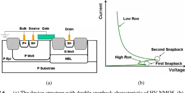
(26) 1.3.4. The Substrate-Triggered Technique. The substrate-triggered technique is to draw an electric connection from the P+ of substrate or N+ of N Well [17]. The current flows into the substrate or well can change the turn-on resistance of the ESD protection device during ESD stress. It means the substrate current can change the turn-on area or the turn-on path as parasitic lateral BJT in the NMOS to sustain higher ESD stress. Comparing to the gate-coupled, there is no gate bias to lower the energy bands on the surface channel of the substrate-triggered NMOS. But, the substrate bias can lower the energy bands in the substrate region and extend the current distribution. The turn-on behavior of the substrate-triggered GGNMOS device is the parasitic lateral BJT of all fingers can be uniformly turned on. With the increasing of the substrate current, the trigger voltage and the turn-on resistance of the device can be reduced as shown in Fig. 1.20. The substrate-triggered circuit structure is also use the RC-based detection circuit to trigger the ESD protection device as shown in Fig. 1.21. During the positive ESD stress, the voltage of point A is logic low to trigger the PMOS (Mp1) and let the voltage of point B be logic high. Then, the NMOS (Mn2) is triggered and let the voltage of point C be logic low. The turn on of the Mp1 can conduct the current from VDD to trigger the P+ diffusion of P Substrate; the turn on of the Mn2 can draw the current from the N+ diffusion of N Well to VSS and it means the N Well has been triggered. These two types of substrate-triggered methods can be used in any device to reduce its trigger voltage. For example, the trigger voltage of HV SCR is too high to protect the internal circuit. Moreover, in order to avoid the latchup effect of HV SCR, the stacked-device technique can be adapted to raise the holding voltage, but the trigger voltage is also rise up. The trigger node can be set on the N+ of N Well and P+ of P Substrate to trigger the parasitic NPN and PNP BJTs synchronously. Then, the HV SCR can be triggered on without junction avalanche breakdown mechanism. When the trigger current is applied in p-trigger node, the NPN BJT in the SCR device is active, and the collector current of NPN is generated to bias the PNP transistor. Then, the PNP is turned on, the collector current of PNP is also generated to further bias the NPN transistor. The positive-feedback regenerative mechanism of latchup is initiated by the substrate-triggered current in SCR structure instead of avalanche breakdown mechanism. On the other hand, when the trigger current is drawn from the n-trigger node, the positive-feedback mechanism is also generated. On the whole-chip ESD protection, the double-triggered SCR (including the n-trigger -8-.
(27) and p-trigger) is set between the power-rail, I/O pad to VDD and VSS, respectively. In order to save the layout area, the RC-based ESD detection circuit can be shared and connect to each double-triggered SCR, as shown in Fig. 1.22.. 1.3.5. The Native-NMOS-Triggered Technique. Using the parasitic PMOS structure to trigger the SCR ESD protection device is introduced as above. There is another trigger method by using the native-NMOS with very low threshold voltage about 0.1 V to trigger the SCR device [18]. Compared with the traditional low-voltage-triggered SCR (LVTSCR), the drain of native NMOS in native-NMOS-triggered SCR (NANSCR) is directly coupled to the anode of SCR, but the drain of NMOS in LVTSCR is set across the N Well/P Substrate junction of the SCR device, as shown in Figs. 1.23(a) and 1.23(b), respectively. The gate of native NMOS is connected to a negative bias circuit (NBC) to keep off the NANSCR during normal circuit operation. The NBC is composed of clock generator, capacitors and diodes. The output negative voltage of NBC can be tuned to fulfill various applications. During the ESD event, the NBC is relatively floating, the native NMOS is an initial-on device as the PMOS-triggered SCR. Then, the trigger current flows into the base of NPN and the base voltage of NPN will be raised up by the substrate resistor (Rsub). Once the voltage across the base and emitter of NPN exceeds 0.7 V, the NPN in SCR structure is turned on. After the NPN turns on, the PNP is also turned on by the collector current of NPN. Therefore, the positive-feedback mechanism of the NANSCR is initiated by the trigger current of the initial-on native NMOS in the NANSCR device. Finally, the NANSCR will be triggered on to discharge the ESD current. In addition, comparing with the TLP I-V curve of the LVTSCR and NANSCR, the turn-on resistance and holding voltage of NANSCR are smaller than those of LVTSCR on the same device width.. 1.3.6. The Dummy-Gate Structure Technique. The dummy-gate structure is used to block the shallow trench isolation (STI) and silicide between the diffusion regions as shown in Figs. 1.24(a) and 1.24(b) [19], the ESD current discharge path can be changed to enhance the turn on speed of the ESD protection device. For example, to merge the dummy-gate structure with the substrate-triggered SCR. -9-.
(28) (STSCR) device. Due to the deeper STI region causes a longer current path from the anode to cathode, the dummy-gate structure can block the STI region to smaller the current path. This STSCR with dummy-gate structure can be used in input, output and power-rail ESD protection device. In order to prevent the device suffering latchup, the voltage drop elements (such as diodes) can be stacked with the dummy-gate structure STSCR to raise the total holding voltage. Comparing on the STSCR device with STI and dummy-gate structure, the trigger voltage can be further reduced by the dummy-gate structure than STI structure under the same trigger current. The reason is the current gain (β) of parasitic BJT in dummy-gate structure is higher than in STI structure by the shorter current path.. 1.3.7. The Self-Substrate-Triggered Technique. The self-substrate-triggered technique is to conduct the ESD current to the desired finger location and use the ESD current to trigger other fingers [20]. This trigger method will improve the turn-on uniformity and the HBM and It2 level of the GGNMOS substantially, but the trigger voltage and holding voltage will not change. Due to the base resistance in parasitic NPN of the center-finger GGNMOS is higher than other fingers, the center-finger of GGNMOS is always triggered first. Once the center-finger of NMOS has been triggered, the ESD voltage will let the device into snapback status. Therefore, the ESD current will be only discharged through few part of device to cause the non-uniform turn on issue. In order to guarantee the center-finger of the GGNMOS will turn on first, let the channel length of the center-finger be the minimum rule and other fingers with larger channel length. The cross-sectional view of the self-substrate-triggered GGNMOS is shown in Fig. 1.25, the source of the center-finger is connected to the substrate-triggered node.. 1.4 Thesis Organization In order to reach the desired ESD performance in 0.25μm 18V BCD process, there are various layout splits have been verified in this thesis. This thesis is composed of five chapters. Chapter 1 presents the fundamental concept of ESD protection design by device layout modification and extra trigger circuit. In order to get the appropriate trigger voltage and holding voltage in high voltage operation to protect the - 10 -.
(29) internal circuit and suppress the latchup effect, there are several methods to reduce the trigger voltage and the suitable device structure to avoid the latchup happens In chapter 2, presents an overview on several power MOS transistors and their advantages and disadvantages in current path and reliability. To research one kind of power MOS transistors, the DMOS is the main topic of this thesis. Then, discuss the turn-on mechanism and double-snapback characteristic in HV LD-NMOS and HV NMOS. Such turn-on mechanism is very important on designing the trigger and holding voltage. In chapter 3, presents the HV BJT with controllable trigger and holding voltage, the HV NMOS with Embedded SCR structure and HV BJT with Embedded SCR Structure those have been reported first. Then, the experimental results show the ESD performance of HV LD-NMOS, HV LD-PMOS, HV NFOD, HV dual-direction SCR and HV NSCR by layout modification. The ESD performance of LD-NMOS, NFOD and NSCR can be improved to 2A by increasing the N+ edge to contact spacing of the drain side. The dual-direction SCR can be used in discharging the ESD current while the operation voltage is from negative to positive. With increasing the layout parameters of dual-direction SCR, the It2 value, HBM and MM level can be improved to about 4A, 6KV and 300V, respectively. In chapter 4, presents the failure mechanism of the LD-NMOS and introduce the methods of no turn-on parasitic BJT and no snapback characteristic in LD-NMOS. To make sure the no snapback characteristic can be made correctly, the PSB (P type Sub Body) layer of 0.25μm 18V BCD process is added to let the ESD protection device not to snapback. The PSB layer is verified in small device (total width <5k μm) and large device (total width > 5k μm) to investigate the influence on ESD performance of LD-NMOS. In larger device, the PSB layer can reach the no snapback characteristic and have the best turn-on uniformity. Finally, the main results of this thesis are summarized in chapter 5, the future work is to research the holding voltage is different by TLP and 370A measuring. In addition, the trigger elements have to be added in the dual-direction SCR to reduce the trigger voltage without extra layout area.. - 11 -.
(30) Fig. 1.1. Fig. 1.2. (a). (b). (c). (d). The I-V curve of the four common ESD protection devices: (a) gate-grounded NMOS (GGNMOS), (b) gate-VDD PMOS (GDPMOS), (c) parasitic silicon controlled rectifier (SCR), and (d) diode.. (a). (b). (c). (d). The four pin-combination modes for ESD test: (a) positive-to-VSS (PS-mode), (b) negative-to-VSS (NS-mode), (c) positive-to-VDD (PD-mode), and (d) negative-to-VDD (ND-mode). - 12 -.
(31) Fig. 1.3. The whole-chip ESD protection circuits in CMOS IC.. (a). (b) Fig. 1.4. (c). (a) The parasitic SCR path in CMOS ICs. (b) The equivalent circuit of SCR. (c) The two terminals and four layers P-N-P-N of SCR.. - 13 -.
(32) Fig. 1.5. The latchup-free current gain (β) product parabola curve.. (a). (b). (c) Fig. 1.6. (a) The N+/N Well guard ring, (b) The P+/P Substrate guard ring, (c) The double guard ring.. - 14 -.
(33) (a). (b). (c). (d) Fig. 1.7. The device cross-sectional views of (a) isolated HV NMOS, (b) non-isolated HV NMOS, (c) non-isolated symmetric HV NMOS, (d) isolated asymmetric HV NMOS and HV PMOS. - 15 -.
(34) (a) Fig. 1.8. (b). (a) The stacked power rail ESD protection device and its RC-based detection circuit. (b) The TLP I-V curves of single FOD and stacked-FOD.. (a). (b). (c) Fig. 1.9. (d). (e). (a) ~ (b) The traditional ESD protection device with the initial-off characteristic. (c) ~ (e) The ESD protection device with the initial-on characteristic.. - 16 -.
(35) Fig. 1.10. The ESD protection design window in traditional SCR device.. Fig. 1.11. The cross-sectional view of the initial-on SCR with PMOS trigger technique.. - 17 -.
(36) Fig. 1.12. The equivalent circuit of the initial-on SCR with PMOS trigger.. (a) Fig. 1.13. (b). The layout view of the initial-on SCR with PMOS trigger (a) The common layout pattern, (b) The n-trig node merged into the source side of the embedded PMOS structure. - 18 -.
(37) (a). (b) Fig. 1.14. (c). (a) The cross-sectional view of the dual-direction SCR structure, (b) The trigger node and the trigger method with two pair back-to-back Zener diode, (c) The TLP I-V characteristic of the dual-direction SCR.. - 19 -.
(38) (a). Fig. 1.15. (b). (c). (d). (e). (f). (g). (a) The layout cell structure of the dual-direction SCR, (b) The layout view of corner cell, (c) The layout view of edge cell, (d) The layout view of center cell, (e) The cross-sectional view of corner cell, (f) The cross-sectional view of edge cell, (g) The cross-sectional view of center cell.. - 20 -.
(39) (a). (b). Fig. 1.16. (a) The ESD current always flow through the center-finger of GGNMOS first, (b) The center-finger will burn out by the joule heating.. Fig. 1.17. The gate-coupled structure and the turn-on sequence of the gate-coupled technique.. - 21 -.
(40) Fig. 1.18. The TLP I-V curves of various rising time of the ESD pulse.. (a). (b). (c) Fig. 1.19. (a) The HV NPN BJT, (b) The HV NPN-SCR, (c) The HV NSCR. - 22 -.
(41) Fig. 1.20. The TLP I-V curves and turn-on resistances of the different substrate trigger current on GGNMOS (added trigger current:curve A > curve B > curve C).. Fig. 1.21. The double-substrate-triggered structure (including the P-trigger node and N-trigger node).. - 23 -.
(42) Fig. 1.22. The whole-chip ESD protection with shared ESD detection circuit for input, output and power-rail ESD clamp devices.. (a) Fig. 1.23. (b). The circuit schematics of (a) the native-NMOS-triggered SCR (NANSCR), (b) the traditional LVTSCR.. - 24 -.
(43) (a). (b) Fig. 1.24. The circuit schematics of (a) the native-NMOS-triggered SCR (NANSCR), (b) the traditional LVTSCR.. Fig. 1.25. The cross-sectional view of the self-substrate-triggered GGNMOS. The P+ trigger node connects to the source terminal of the center-finger. - 25 -.
(44) CHAPTER 2 OVERVIER ON POWER MOSFETs FOR HIGH-VOLTAGE ESD PROTECTION DESIGN. 2.1 Power MOS Transistors MOS transistors can drive large amounts of power are called power transistors to distinguish them from low-power or small-signal devices. The power MOS can conduct large currents at low drain-to-source voltage by the low impendence characteristic. At low drain-to-source voltage (VDS<<VGS-Vt), the Shichman-Hodges equation in the linear region will be derived from Id=k(VGS-Vt)VDS+kVDS2/2 to Id=k(VGS-Vt)VDS. The on resistance RDS(on) varies inversely with the product of the transconductance and the effective gate voltage (VGS-Vt), it will be RDS(on)=1/k(VGS-Vt). The RDS(on) of the power MOS transistors are usually measured at a specified gate voltage VGS and junction temperature. The RDS(on) of a power MOS transistor typically increases 50% when the junction temperature rises from 25℃ to 125℃. The metallization resistance becomes significant for on resistance of less than an Ohm order, and the equation for RDS(on) then becomes RDS(on) =1/k(VGS-Vt)+RM. Where the RM is the sum of the resistance of the source and drain metallization. This metallization resistance is difficult to calculate because it depends on transistor geometry. There are several metal line layout patterns have been published as shown in Figs. 2.1(a) ~ 2.1(c). Fig. 2.1(a) shows a common arrangement in which both terminations lie on the same side of the transistor. The paired terminations may be more adjacent to the bond pads, but they produce excessive voltage drop and an uneven distribution of current in the device. Fig. 2.1(b) shows a better arrangement where the source and drain terminations lie on the opposite sides of the transistor. This arrangement delivers a more even distribution of current and exhibiting a lower total resistance than the pattern in Fig. 2.1(a). Fig. 2.1(c) shows the method to minimize the metallization resistance. The termination points lie on the middle of both buses, so the current does not have to flow through the full length of the buses.. - 26 -.
(45) The smart power integrated circuit technology is composed of VLSI digital/analog signal processing and high power output current driver on the same chip. The percentage split in chip area is uncommonly by 50% to 50% each. The signal processing part is consist of low voltage (LV) circuits;The power output current driver usually operates in high voltage (HV) and/or high current supply. The smart power integrated circuit technology applies in Automotive Electronics, Telecommunications, Power management, LCD (Liquid Crystal Display) or EL (Electro Luminescence) industry, etc [21]. Especially the large number of column and row drivers of the LCD industry, the driving speed in dependent on the frame rate and scan rate of the display. For a refresh frame rate of 60 frames per second on the VGA definition (640 x 480), a minimum scan rate of 30 kHz is needed. For these reasons, MOS technology is preferred to approach these performances. How to improve the density and switching speed of the high voltage output transistors is the main challenge in the next generation of high-definition (HD) performance. Power devices in smart power integrated circuit technology are usually required to perform switching functions. The gate drive characteristic of the MOSFETs is more favorable than the bipolar junction transistors (BJTs) with large base current to turn on/off. One of the main advantages of power MOSFETs is that the gate only requires a bias voltage with no steady-state current to switch between the on and off states. Due to above reasons, the inherent switching speed of MOSFETs is faster than for power BJTs. Most high voltage devices are used as switches operating between the on and off states and designed to operate in the 1st quadrant, occasionally in the 3rd quadrant as shown in Fig. 2.2. The I-V curve is similar to the conventional MOSFETs except that the power devices usually switch between fully on and fully off – cutoff or triode region. The power devices rarely operate in the saturation region (except as amplifiers) because of power dissipation limits. Power MOSFETs can be categorized into V-MOS, VDMOS, UMOS, IGBT and LDMOS. The V-MOS have a V-groove etch from the top side of the wafer using a preferential etch and the channel is formed along the wall of the V-groove as shown in Fig. 2.3(a). The V-MOS was the first commercial power MOSFET structure, however it is quickly replaced by the VDMOS due to manufacturing problems and the concentration of high electric field at the tip of the V-groove. The VDMOS has a conventional surface channel while still relying on double diffusion to produce the short channel length as shown in Fig.. - 27 -.
(46) 2.3(b). The UMOS uses a trench etching technique to turn the channel into a vertical direction as shown in Fig. 2.3(c). In the V-MOS, VDMOS and UMOS, the forward blocking capability is provided by the P Well to N Epi junction. Due to higher doping concentration of the P Well region, the depletion region extends mostly into the N Epi region. Therefore, the choice of N Epi doping concentration can directly affects the breakdown voltage and on-resistance of the power MOSFETs. The IGBT (Insulated Gate Bipolar Transistor) is use the P+ substrate to replace the N+ substrate and then a merged MOS-Bipolar device can be made as shown in Fig. 2.3(d). The IGBT offers enough amounts of current handling capability, but with slower switching speed. The IGBT is a dominant power device in high current application. The V-MOS, VDMOS, UMOS, IGBT as above are vertical devices, the drawback of the vertical devices is that it is difficult to include multiple power devices on the same chip. But the lateral structure allows all terminals to be accessed from the top surface of the chip. The current flows from the drain, laterally along the surface through the MOS channel and up into the source, hence the name Lateral Double-Diffused MOSFETs (LDMOS) as shown in Fig. 2.4(a) [22]-[25]. LDMOS generally has a higher on-resistance due to the longer current path than vertical devices. Furthermore, the breakdown voltage of the LDMOS depends critically on the curvature of the P Well to N Drift region junction. In order to obtain high breakdown voltage, it is necessary to use a low doping concentration in the N Drift region. However, this will cause a high turn-on resistance. To provide a device with high breakdown voltage and low turn-on resistance, an advanced technique called REduced SURface Field (RESURF) was developed as shown in Fig. 2.4(b) [26]-[27]. The RESURF device structure is the same as the LDMOS, except the much thinner N Epi layer is added for the N Drift region. Through a well-tuning doping concentration in the N Drift region, a much lower turn-on resistance can be produced without decreasing in breakdown voltage. The breakdown voltage of LDMOS is mainly between 20 V to 100 V and is more suitable for automotive applications. The remaining issue is to reduce the series resistance of the metal interconnection and bonding wires. Due to the specific lower on-resistance and high breakdown voltage, the LDMOS can as for output current driver and self high-voltage ESD protection device simultaneously. This chapter will discuss the whole mechanisms of the LDMOS including the turn-on mechanism, the double-snapback characteristic and the isolation method to implement the high breakdown voltage. - 28 -.
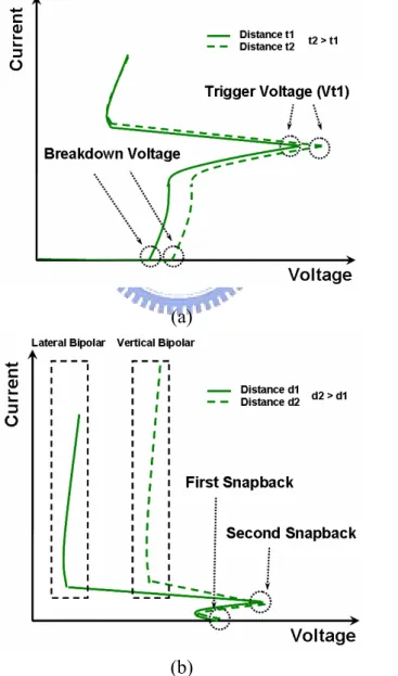
(47) 2.2 The Turn-On Mechanism and Double-Snapback Characteristic of the High-Voltage LD-NMOS and High-Voltage NMOS Devices The turn-on mechanism of the LD-NMOS device is caused by the positive feedback between the turn-on BJT of the source side and the N/N+ junction avalanche breakdown of the drain side and it’s called the double snapback characteristic. Although the N/N+ junction is the most basic parasitic structure in the device, which plays a major role in the snapback characteristic. In order to analyze the I-V curve of the LD-NMOS structure, there are three points that have been sampled as shown in Fig. 2.5(a). Point A denotes the turn-on BJT of the source side and the point C denotes the N/N+ junction avalanche breakdown of the drain side. With increasing the applied voltage in the drain side, the more excess electrons from the N+ source induce the more excess holes from N+ drain in the HV N Well/P Body junction. These space charges will become denser at the junction and raise the electric field. Moreover, one part region of the HV N Well with excess holes become an extension of the P Body layer. In other words, this effect is the same as the “Kirk effect [28]-[29]” of the BJT and the extension region will reach the N+ drain region until the excess electrons concentration is less than the N+ drain doping concentration. As a result, the electrical field peak moves from the HV N Well/P Body junction to the N/N+ junction of the drain side, as shown in Fig. 2.5(b). This electric field peak leads the N/N+ junction avalanche breakdown and feedbacks additional hole current to the P Body. The electric field of point A is large enough to trigger the impact ionization effect and the electric field of point B will enhance the ionization. Due to the avalanche multiplication occurred in the HV N Well/P Body junction, the voltage to sustain the junction breakdown is reduced, and then it snapbacks to low voltage and causes a negative slope after point A. Point C denotes the electric field peak reaches the N/N+ junction to cause the junction avalanche breakdown. Then, the feedback hole current will improve the multiplication effect in the HV N Well/P Body junction and snapback to low voltage again. Compared to other structure of HV device, the HV NMOS with deeper N Well and N+ Buried Layer (NBL) can also have the double snapback characteristic, as shown in Fig. 2.6(a). Due to the doping concentration of the NBL is higher than the N Well region, the breakdown - 29 -.
(48) voltage is determined by the NBL/P Well junction and the first snapback is caused by the turn-on of BJT. After turn-on the BJT, the current flows vertically into the NBL region will result in a longer current path and the turn-on resistance will become larger. When the current further increases, the “Kirk effect” happens and the electric field peak moves from NBL/P Well junction to N Well/N+ junction. Then, the N Well/N+ junction will go into avalanche breakdown and increase the multiplication rate to snapback to lower holding voltage, as shown in Fig. 2.6(b). The current path of this HV structure will be changed from vertical path to lateral path and get a smaller turn-on resistance after the second snapback. But not all HV devices have the double snapback characteristic [30], if the current path will not change, the second snapback characteristic will be not obvious or be no longer exist. Figs. 2.7(a) and 2.7(b) show the HV device structure without the double snapback characteristic and its TLP I-V curve. The shallow N Grade region is to sustain the high breakdown voltage, before and after the N Grade/P Well junction breakdown, the current path is always in the lateral direction.. 2.3 The Isolation Technique of High-Voltage Devices There are two isolation techniques have been reported to reach the high breakdown voltage. The first isolation method is called the self isolation. It is mostly used in MOS technology and the source and drain junction isolate by itself under reverse bias, as shown in Fig. 2.8(a). In addition, the potential of source will be always grounded. The second isolation method is called the junction isolation, the device will be enclosed by the PN junction and the potential of source may be above ground potential, as shown in Fig. 2.8(b). With such kinds of isolation technique, the trigger voltage of the ESD protection device can be increased and resist the external noises.. - 30 -.
(49) (a). (b). (c) Fig. 2.1. Three kinds of layout patterns and its current flow path (a) The layout structure of the same side current flow, (b) The layout structure of the opposite side current flow, (b) The layout structure of the minimum metallization.. Fig. 2.2. The operation region of the power transistors. - 31 -.
(50) (a). (b). (c). Fig. 2.3. (d). Four kinds cross-sectional views of power devices: (a) The VMOS device, (b) The VDMOS device, (c) The UMOS device, (d) The IGBT device.. (a). Fig. 2.4. (b). (a) The LDMOS device, (b) The RESURF device. - 32 -.
(51) (a). (b) Fig. 2.5. (a) The three TLP I-V sampled points of LD-NMOS, (b) The electric field distribution versus the applied current.. (a) Fig. 2.6. (b). (a) The device structure with double snapback characteristic of HV NMOS, (b) The TLP I-V curve of device structure with double snapback characteristic of HV NMOS. - 33 -.
(52) (a). Fig. 2.7. (b). (a) The device structure without double snapback characteristic of HV NMOS, (b) The TLP I-V curve of device structure without double snapback characteristic of HV NMOS.. (a). Fig. 2.8. (b). (a) The self isolation structure, (b) The junction isolation structure.. - 34 -.
(53) CHAPTER 3 DEVICE PARAMETERS MODIFICATION FOR HIGH-VOLTAGE ESD PROTECTION DESIGN. The high-voltage (HV) ESD protection devices should be provided with a higher breakdown voltage than operation voltage to guarantee they won’t be triggered in normal circuit operation. The method of providing a higher breakdown voltage is usually through a low doped layer under the drain side. This chapter will introduce some HV devices that have been reported and present the experimental results of HV LD-NMOS, HV LD-PMOS, HV N-type Field Oxide Device (NFOD), HV Dual-Direction Silicon Controlled Rectifier (DD-SCR) and HV NMOS with embedded SCR (NSCR) in a 0.25μm 18V BCD technology.. 3.1 The High-Voltage ESD Protection Devices There are several high-voltage ESD protection devices that have been developed in different two processes. In the high-voltage (HV) process, a low doping layer is added in the drain and source sides named DDD-structure to increase the breakdown voltage. The ESD robustness of the asymmetric structure is better than symmetric structure in the HV process as described in chapter 1. The asymmetric structure means the DDD layer is added in the drain side. In the Bipolar-CMOS-DMOS (BCD) process [31]-[35], there are BJT, CMOS and DMOS to use in the high-voltage operation. In addition, the diode with high reverse breakdown voltage and high-voltage SCR are also available in these two processes.. 3.1.1. The High-Voltage Bipolar Junction Transistor with Controllable Trigger and Holding Voltage. To provide effective whole-chip ESD protection, on-chip ESD protection devices are added in different parts of ICs. The required ESD specification of breakdown voltage, trigger - 35 -.
數據


+7
相關文件
A factorization method for reconstructing an impenetrable obstacle in a homogeneous medium (Helmholtz equation) using the spectral data of the far-field operator was developed
A factorization method for reconstructing an impenetrable obstacle in a homogeneous medium (Helmholtz equation) using the spectral data of the far- eld operator was developed
After students have had ample practice with developing characters, describing a setting and writing realistic dialogue, they will need to go back to the Short Story Writing Task
Now, nearly all of the current flows through wire S since it has a much lower resistance than the light bulb. The light bulb does not glow because the current flowing through it
In view of the large quantity of information that can be obtained on the Internet and from the social media, while teachers need to develop skills in selecting suitable
– For each k, the faster, smaller device at level k serves as a cache for the larger, slower device at level k+1. • Why do memory
A smaller aperture increases the range in which A smaller aperture increases the range in which the object is approximately in focus. Di
Model checking: residuals can be obtained by 1-step ahead forecast errors at each time point, (observations minus the fitted value) Then if the model is adequate, residuals should
