國
立
交
通
大
學
電子工程學系 電子研究所
碩
士
論
文
應用於微瓦特動態電壓與頻率調節系統設計中近/次
臨界電壓具製程電壓溫度能力之感測器
Near-/Sub-threshold PVT Sensors for Micro-Watt DVFS
System Design
研 究 生:陳璽文
指導教授:黃 威 教授
應用於微瓦特動態電壓與頻率調節系統設計中近/次
臨界電壓具製程電壓溫度能力之感測器
Near-/Sub-threshold PVT Sensors for Micro-Watt DVFS
System Design
研 究 生:陳璽文 Student:Shi-Wen Chen
指導教授:黃 威 教授 Advisor:Prof. Wei Hwang
國 立 交 通 大 學
電 子 工 程 學 系 電 子 研 究 所
碩 士 論 文
A Thesis
Submitted to Department of Electronics Engineering & Institute of Electronics College of Electrical Engineering and Computer Engineering
National Chiao Tung University in partial Fulfillment of the Requirements
for the Degree of Master
in
Electronics Engineering June 2009
Hsinchu, Taiwan, Republic of China
中華民國九十九年七月
應用於微瓦特動態電壓與頻率調節系統設計中近/次
臨界電壓具製程電壓溫度能力之感測器
學生:陳璽文
指導教授:黃 威 教授
國立交通大學電子工程學系電子研究所
摘 要
在本篇論文中,我們將目標放在設計並實現一個應用於微瓦特動態電壓與頻率 調節系統設計中具製程電壓溫度能力之感測器。其中包含自動補償全數位之製程 電壓溫度感測器、多臨界電壓互補式金屬氧化層半導體(MTCMOS)之交換式電容 直流-直流轉換器、具數位溫度補償之低電壓鎖相迴路頻率產生器、動態電壓與 頻率調節系統。主要的研究成果如下: 1. 提出了一個可以操作在近臨界/次臨界電壓的全數位溫度感測器,具備有 高精準度、電壓小、耗電低、自動補償等優點。 2. 提出了一個利用可調性脈衝寬度產生器去自動補償溫度感測器受電壓製 程影響且可以操作在近臨界/次臨界電壓的數位溫度感測器,具備有高精 準度、電壓小、耗電低等優點。 3. 在本篇論文中提出了一個可應用於微瓦特系統中具製程電壓溫度感知的 動態電壓與頻率調節系統。本系統透過交換式電容直流-直流轉換器可以 提供非常穩定直流電源,產生不同的電壓位準透過動態電壓轉換電路做電壓調節。並且透過溫度感測器在不同溫度下選擇不一樣的電壓,可有效的 減少功率消耗和維持系統運作的穩定度。 4. 一個新的架構用於提升交換式電容直流-直流轉換器在低負載時的能量效 益和電壓穩定度被提出。 5. 在本篇論文中提出一個具數位溫度補償之低電壓鎖相迴路頻率產生器,可 以透過除頻器去調節輸出頻率,以及用溫度去補償最壞情況下頻率無法鎖 住的問題。
Near-/Sub-threshold PVT Sensors for Micro-Watt DVFS
System Design
Student : Shi-Wen Chen
Advisors : Prof. Wei Hwang
Department of Electronics Engineering & Institute of Electronics
National Chiao-Tung University
ABSTRACT
The goal of this research is to design and implement PVT sensors for micro-watt DVFS system design. It includes the design of self-calibration all-digital PVT sensors, MTCMOS switched capacitor (SC) DC-DC converter, temperature compensation for low-voltage digital assist PLL, and dynamic voltage and frequency scaling system. The major contributions are as below:
1. A near-/sub-threshold all-digital process, voltage, and temperature sensor is proposed and integrated to the DVFS control for micro-watt system applications. The sensor is proposed for high accuracy, ultra-low voltage, low power, and self-calibration portable applications.
2. A self-calibration near-/sub-threshold all-digital temperature sensor with adaptive pulse width generator is proposed. The sensor is proposed for high accuracy, ultra-low voltage, low power, and self-calibration portable applications.
3. A PVT-aware DVFS for micro-watt system is proposed. The system through the switched capacitor (SC) DC-DC converter can provide a very stable DC power supply. It generates different voltage levels which are suitable for SoC integrated regulator applications.
4. A novel connect scheme for improving power efficiency and reducing voltage variation of switched capacitor (SC) DC-DC converter which generates ultra low voltage is proposed.
5. Proposed a temperature compensation for low voltage digital assist PLL can modulate output frequency via divider. Use the temperature sensor to compensate the frequency can not lock in the worth case.
Content
摘 要... i
ABSTRACT ... iii
Content ... v
List of Figures ... vii
List of Tables ... x
Chapter 1 Introduction ... 11
1.1 Motivation of the Thesis ... 11
1.2 Research Goals and Major Contributions ... 3
1.3 Thesis Organization ... 4
Chapter 2 Previous of Process, Voltage, and Temperature sensors ... 6
2.1 Conventional Process Sensor ... 6
2.2 Voltage Sensor Circuit Evolution... 9
2.3 Temperature Sensor Circuit Evolution ... 15
2.4 PVT Sensors Applications ... 29
2.5 Summary ... 35
Chapter 3 Fully On-Chip Process, Voltage, and Temperature Sensors ... 36
3.1 Time to Digital Converter (TDC) Architecture ... 37
3.2 Frequency to Digital Converter (FDC) ... 38
3.3 Fixed Pulse Width Generator ... 39
3.4 Zero Temperature Coefficient Point Application – Process Sensor ... 41
3.5 A Fully Digital Voltage Sensor Using A New Delay Element ... 45
3.6 Fully On Chip Ultra-Low Voltage Temperature Sensor ... 46
3.7 1-point Calibration Method of Proposed Temperature Sensor ... 50
3.8 Conclusion and Simulation Results ... 52
3.9 Summary ... 54
Chapter 4 Self-Calibration Method for Subthreshold All-Digital PVT Sensors .. 55
4.1 Previous TDC Calibration Method ... 55
4.2 Proposed Self-Calibration Method for Subthreshold All-Digital PVT Sensors ... 60
4.3 Ultra-Low Voltage All-Digital Temperature Sensor with Adaptive Pulse Width Compensation ... 67
4.4 Summary ... 74
Chapter 5 PVT Sensors for Micro-Watt DVFS System Design ... 75
5.1 PVT Sensors for Micro-Watt DVFS System Design ... 76
5.2 Switched Capacitor DC-DC Converter ... 77
5.4 Post-Layout Simulation Results... 96
5.5 Temp. Compensation for Low-voltage Digital Assisted PLL ... 102
5.6 Summary ... 106
Chapter 6 Concludions and Future Work ... 108
6.1 Conclusions ... 107
6.2 Future Work ... 107
List of Figures
Figure 1.1. Sensor network of WBAN... 11
Figure 1.2 Dynamic voltage and frequency scaling systems ... 3
Figure 2.1. Process monitoring circuit. ... 8
Figure 2.2. Process dependence of reference voltage (output) in different temperatures and supply voltages: (a) VDD = 0.8 V; (b) VDD = 0.9 V; (c) VDD = 1.0 V. ... 8
Figure 2.3 Successive Approximation ADC Block Diagram... 11
Figure 2.4 The general all-digital ADC. ... 12
Figure 2.5 Quantization levels of ADC. ... 12
Figure 2.6 All-digital voltage to frequency converter ADC. ... 13
Figure 2.7 Voltage to time conversion concept using digital circuit. ... 14
Figure 2.8 Voltage to time conversion wave signals. ... 14
Figure 2.9 Conventional three-transistor temperature sensor. ... 17
Figure 2.10 Operating-point comparison of three-transistor temperature sensor on IDS-VGS curves at 1.8- and 1.0-V supply voltage. ... 18
Figure 2.11 Four-transistor, voltage output, temperature sensor. ... 19
Figure 2.12 Operating points of four-transistor temperature sensor. ... 20
Figure 2.13 Conventional digital output of temperature sensor. ... 21
Figure 2.14 Block diagram of the time-to-digital temperature sensor. ... 21
Figure 2.15 Temperature-to-pulse generator. ... 23
Figure 2.16 Width offset reduction accomplished by delay line 2. ... 23
Figure 2.17 Delay cell is used in delay line 2. ... 24
Figure 2.18 Block diagram of the cyclic TDC. ... 25
Figure 2.19 Basic architecture of DLL-based CMOS digital temperature sensor. ... 27
Figure 2.20 Calibration mode (top) and measurement mode (bottom). ... 27
Figure 2.21 DLL-based CMOS all-digital temperature sensor. ... 28
Figure 2.22. The oscillation frequency of ring oscillator with and without temperature-driven control scheme for self-refresh of DRAM ... 30
Figure 2.23. Circuit diagram of DRAM self-refresh control scheme with temperature sensor ... 30
Figure 2.24.Temperature effect on rising edge skew between buffers T3_4 and T4_2. ... 32
Figure 2.25. 3D clock tree with via. ... 32
Figure 2.26. Thermally adaptive buffer schematic. ... 33
Figure 2.28. (a) Temperature monitoring circuit. (b) Process monitoring circuit. ... 35
Figure 3.1 A basic TDC architecture. ... 37
Figure 3.2 A vernier delay line TDC. ... 38
Figure 3.3 Frequency-to-digital converter (FDC) Architecture. ... 39
Figure 3.4 Fixed pulse generator block diagram and wave form. ... 40
Figure 3.5 simulation result of fixed pulse generator. ... 40
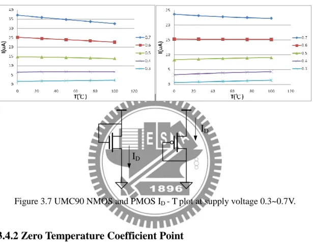
Figure 3.6 MOS current equation in saturation mode ... 41
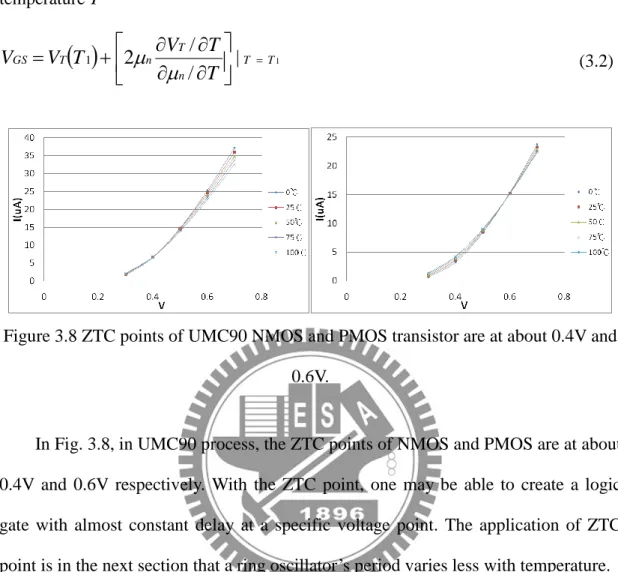
Figure 3.7 UMC90 NMOS and PMOS ID - Tplot at supply voltage 0.3~0.7V. ... 42
Figure 3.8 ZTC points of UMC90 NMOS and PMOS transistor are at about 0.4V and 0.6V. ... 43
Figure 3.9 At 0.5V, NMOS ID decreases with T, PMOS ID increases with T. ... 44
Figure 3.10 Ring oscillator’s frequency – temperature plot in corners FF, TT, SS. .... 44
Figure 3.11 Process Monitor circuit. ... 44
Figure 3.12 Ring oscillator’s frequency with process variation. ... 45
Figure 3.13 A fully digital voltage sensor. ... 46
Figure 3.14 Proposed fully on chip temperature sensor. ... 49
Figure 3.15 Bias current generator. ... 49
Figure 3.16 (a) Simulation result of temperature sensor with voltage variation. (b) Simulation result of temperature sensor with process variation. ... 50
Figure 3.17 (a) Simulation result of temperature sensor with voltage variation. ... 52
Figure 3.18 1-point Calibration Method of Temperature Sensor. ... 52
Figure 4.1 (a) Typical setup for direct calibration of an arbitrator. ... 56
Figure 4.2 (a) Portion of a conventional VDL-based TDC. (b) Equivalent circuit containing a single delay line with an added AND gate for calibration. ... 58
Figure 4.3 Proposed all-digital temperature sensor... 61
Figure 4.4 Simulation result of proposed temperature sensor in different supply voltage. ... 63
Figure 4.5 Simulation result of temperature sensor in different process corner. ... 63
Figure 4.6 Proposed all-digital self-calibration PVT sensors. ... 63
Figure 4.7 Self- Calibration circuit of all-digital PVT Sensors. ... 63
Figure 4.8 Simulation results of calibration of temperature sensor in different process corner... 65
Figure 4.9 Layout views of the all-digital PVT Sensors ... 63
Figure 4.10 Architecture of FDC-based CMOS all-digital temperature sensor. ... 63 Figure 4.11 (a) Simulated frequency of ring oscillator in different process corner. (b)
width compensation.. ... 78
Figure 5.1 PVT sensors for micro-watt DVFS system.. ... 78
Figure 5.2 Architecture of the switched capacitor DC-DC converter system. ... 78
Figure 5.3 Topologies used to generate a wide range of load voltages from a 1.2V supply. ... 78
Figure 5.4 Equivalent circuit of the gain configuration with gain of 1/2. ... 79
Figure 5.5 Conventional CMOS bandgap voltage reference. ... 82
Figure 5.6 Automatic frequency scaling circuit. ... 84
Figure 5.7 Energy loss mechanisms in a switched capacitor DC–DC converter. ... 85
Figure 5.8 Efficiency plot with change in load voltage. ... 87
Figure 5.9 Architecture of switched capacitor DC-DC converter. ... 87
Figure 5.10. Switch matrix and simplified representation of the switch size control. . 89
Figure 5.11. DC-DC converter efficiency while delivering 300 mV ... 90
Figure 5.12. Delay line comparator ... 90
Figure 5.13. Proposed Bandgap Voltage Reference (BVR). ... 93
Figure 5.14. Simulated temperature dependence of an NFET and PFET. ... 94
Figure 5.15. Simulated VREF versus temperature. ... 94
Figure 5.16 Resistor-string DAC for variable voltage reference generation. ... 95
Figure 5.17 Variable voltage reference generation with temperature variation. ... 95
Figure 5.18 Layout view of the SC DC-DC converter. (a) with MOS capacitor in UMC 65nm CMOS tech. (b) with MOM capacitor in TSMC 65nm CMOS tech. ... 98
Figure 5.19 The layout of the Power MOS (a) with better ESD protection (b) with better efficiency of area... 100
Figure 5.20 The equivalent MOS of layout in Fig. 5.18(a) and(b). ... 100
Figure 5.21 The transient response of SC DC-DC converter... 100
Figure 5.22 Architecture of phase lock loop (PLL).. ... 100
Figure 5.23 Simulation results of VCO output frequency in different environment condition.. ... 100
Figure 5.24 Architecture of proposed temp. compensation for low-voltage digital assisted PLL.. ... 100
Figure 5.25 Simulation results of VCO output frequency in different environment condition with temperature compensation.. ... 100
Figure 6.1 (a) Block diagram of Near/Sub- threshold FIFO memory. (b) Proposed 8T Near/Sub-threshold SRAM cell…..………... 100
Figure 6.2 (a) ULV MTCMOS SC DC-DC converter. (b) Smart dynamic voltage scaling converter……… 100
Figure 6.3 (a) Self-calibration temperature sensor with adaptive pulse width generator. (b) DTM algorithm……….. 100
List of Tables
Table 2.1 The output of voltage-to-time conversion ADC ... 14
(TD1 >TD2 >TD3 >TD4 >TD5) ... 14
Table 3.1 Voltage Sensor Digital Code Table ... 46
Table 3.2 Temperature sensor comparisons ... 54
Table 4.1 Temperature sensor comparisons ... 74
Table 5.1 Temperature variation ... 96
Chapter 1 Introduction
1.1 Motivation of the Thesis
Wireless microsensor network (WSN) technology creates enormous possibility to have a positive impact on our near future life [1.1]-[1.2]. Advances in ultra-low voltage (ULV) circuit design have recently demonstrated capabilities compatible with wireless body area sensor networks (WBASNs) needs. An important application of WBAN is the vital sensor network shown in Fig1.1. Sensor nodes that measure biomedical signals such as electrocardiogram, blood pressure, and etc, are small pieces either attached on or implanted into a human body. They use a battery with as thin and light characteristics as possible. Most of them do not have the ability to last for a long time. As a result, the demand for low power has been critical in a WBAN. For the health-care purpose, it makes sense when the observation period could last for days to weeks. Therefore, the ultra-low power wireless sensor node (WSN) is the most crucial design target to achieve.
The power reduction is an important design issue for the WBAN. For ultra-low power circuit design, transistors will operate in near/sub-threshold region [1.3]. Lowering the supply voltage and frequency is one of the attractive approaches to reduce power consumption.
Furthermore, dynamic voltage and frequency scaling (DVFS) shown in Fig.1.2, achieves extremely efficient energy saving by adjusting system supply voltage and frequency depending on workload monitor [1.4]. Because if this reason, there are many previous researches about DVFS power management for digital systems such as RISC, DSP and Video Code.
Figure 1.2 Dynamic voltage and frequency scaling systems.
As we continue to reduce the voltage until the transistor get into the near/sub-threshold voltage, circuits will become more sensitive to PVT variations than super threshold. Thus, minimizing energy dissipation and improving variation immunity are far more important rather than operating frequency. Thus, a process,
Since wearable sensors are intended to be worn on the body, miniaturization and minimal weight are important [1.5], [1.6]. Energy harvesting and 3D integration have the potential to solve above mentioned challenges. Energy harvesting [1.7] can exploit the external environment as a source of energy for sensor nodes operating over a full lifetime; while 3D integration [1.8], [1.9] can stack more die connected with a very high packing density of one chip. Through-silicon via (TSV) technology, however, led to higher power density that is much worse hot spot issues. Thus, a PVT-aware micro-watt DVFS system for energy harvesting is also essential.
1.2 Research Goals and Major Contributions
The goal of this research is to design and implement PVT sensors for micro-watt DVFS system shown in Fig.1.3. It includes the design of self-calibration all-digital PVT sensors, MTCMOS switched capacitor (SC) DC-DC converter, temperature compensation for low-voltage digital assist PLL, and dynamic voltage and frequency scaling system.
The major contributions of this thesis are list as follow:
1. A near-/sub-threshold all-digital process, voltage, and temperature sensor is proposed and integrated to the micro-watt DVFS system. The sensor is proposed for high accuracy, ultra-low voltage, low power, and self-calibration portable applications.
2. A self-calibration near-/sub-threshold all-digital temperature sensor with adaptive pulse width generator is proposed. The sensor is proposed for high accuracy, ultra-low voltage, low power, and self-calibration portable applications.
3. A novel connect scheme for improving power efficiency and reducing voltage variation of switched capacitor(SC) DC-DC converter which generates ultra low voltage is proposed.
4. To proposed a temperature compensation for low voltage digital assist PLL can modulate output frequency via divider. Use the temperature sensor to compensate the frequency can not lock in the worth case.
VDDCORE VDD VDDH=0.5V VDDL=0.4V~0.2V DVFS CTRL MTCMOS SC DC-DC Converter workload DVFS Module XTAL Digital assisted PLL CLK N TS volt_level PVT Sensors
Figure 1.3 Proposed PVT sensors for micro-watt DVFS system.
1.3 Thesis Organization
shortcomings of conventional PVT sensors are introduced. The applications of PVT sensors are also introduced.
The organization of the thesis is as below. The Chapter 1 is an introduction and motivations for research. Then, in chapter 2, introduces an overview of conventional process, voltage, and temperature sensors. The detail circuits of conventional process, voltage, and temperature sensors are introduced in this chapter and which also includes the shortages of conventional PVT sensors and the applications of PVT sensors.
In chapter 3, we have as following ideas. First, proposed fully on chip and fully digital PVT sensors. Second, we presented novel FDC technique for PVT sensors, and it can reduce power and area. Also at the same time, it improves temperature linearity in near/sub-threshold region.
The self-calibration all-digital PVT sensors and the self-calibration temperature sensor with adaptive pulse width compensation are proposed in Chapter 4. We use all-digital circuit to replace the traditional PVT sensors which can reduce power consumption and area. And to propose self-calibration technology does not require additional circuitry to achieve high accuracy.
PVT sensors for micro-watt DVFS system is introduced in the final chapter. We combine with previous proposed PVT sensors and DVFS system to control the output voltage of SC DC-DC converter for achieving the reduction of power consumption in different PVT variation. And use PVT sensors to compensate the output frequency of low voltage PLL can not lock in the worth case.
Chapter 2 Previous of Process, Voltage,
and Temperature sensors
This chapter introduces the overview of PVT sensors in power management system. The conventional process sensor design would be demonstrated in Section 2.1. The conventional voltage sensor circuit evolution would be introduced in Section 2.2. Section 2.3 introduces the temperature sensor circuit evolution. Section 2.4 introduces the power management system for PVT sensors applications. Finally, Section 2.5 is the summary.
2.1 Conventional Process Sensor
Technology scaling beyond 90 nm is causing higher level of process variations, which changes the design paradigm from deterministic to probabilistic.
Fig. 2.1 shows a process monitor circuit [2.1]. The circuit consists of a current reference circuit, IR1 generator, and circuits to generate temperature insensitive VOutput.
The current IR1 in Fig. 2.1 is given by
1 1 1
R
V
I
R
GS (2.1)The current IMP4 is determined by the IR1 and the ratio of the transistor MP2 and
MP4. Therefore, VOutput is given by
3 2 4 2 3 3 4 3 4 4
(
)
R MP MP R R R R OutputI
V
R
V
R
V
I
R
V
(2.2) Where β is the transistor aspect ratio.4 3 3 2 2 3 GS R GS MP MP
R
V
V
V
(2.4) If transistor MN3 and MN4 are in subthreshold region, VR3 is obtained by solvingthe (2.4) using the current mirror relationshipsamong IR1, IMP3, and IMP4, and it is
given by
)
ln(
4 3 3 4 1 1 2 2 3 3 MP MP MN MN T GS MP MP RV
V
R
R
V
(2.5)By substituting (2.1) and (2.5) in (2.2), VOutput is obtained as follows:
T GS Output
C
V
C
V
V
1 1
2 (2.6) where 2 4 1 2 2 3 1 2 3 4 1(
1
)
MP MP MP MPR
R
R
R
R
R
C
(2.7))
ln(
)
1
(
2 3 3 4 3 4 2 MP MP MN MNR
R
C
(2.8) In [2.2], VGS1 is given by)
1
(
)
(
0 0 1 1
T
T
K
T
V
V
GS GS G (2.9) where)
(
)
(
T
0V
T
0V
K
K
G
T
GS
th (2.10) where VT is the thermal voltage, KT is the temperature coefficient for thresholdvoltage (typical value is 0.3 V), and T0 is the room temperature.
Substituting (2.10) in (2.6) to find temperature independent VOutput, taking partial
derivative with respect to temperature, and setting it zero
0
T
V
Output (2.11)Solving (2.11), the condition nullifying the temperature coefficient VOutput of is given by G T
K
T
V
C
C
(
0)
2 1
(2.12) However, from (2.12), the temperature coefficient is affected by the large [threshold-voltage variation in different process corner and it leads significant variation of reference voltage. Therefore, the circuit is not suitable for a voltage-reference circuit but is suitable for a process-variation monitoring circuit. Fig. 2.2 demonstrates linear variation of the reference voltage according to process corner conditions. The reference voltage is not affected by temperature and supply voltage variations as shown in Fig. 2.2.2.2 Voltage Sensor Circuit Evolution
Advanced systems (automobiles, medical and other electronic devices) have come to use multiple sensors in recent years, and the number is expected to increase even more in the future. The basic structure of the sensors includes a sensing element and electronic circuits. User requirements for sensors have become more and more demanding, including the need for high performance and lower cost.
Therefore, there are four major problems in predicting the analog type sensors of the near future. The first issue, from an economic perspective, is the difficulty of shrinkage due to loss of accuracy. The second problem involves greater sophistication of, for example, self-correction and self-diagnostics. The third issue is environmental durability. The fourth problem relates to improving reliability.
Research on digitalization of sensor circuits has become energized as efforts are made to resolve these problems. To realize digital sensing, the weak signal from the element must be analog-to-digital (A/D) converted at an early stage within the sensor chip, so an A/D converter (ADC) is required. A successive approximation ADC is a type of analog-to-digital converter that converts a continuous analog waveform into a discrete digital representation via a binary search through all possible quantization levels before finally converging upon a digital output for each conversion.
2.2.1 Successive Approximation Analog-to-Digital Converter
The successive-approximation (SA) ADC is one of the most popular architectures for data-acquisition applications, especially when high-resolution, low power and medium speed are required. In some applications such as wireless sensor nodes, designing low power and low energy ADC is one of the major challenges. For
switching in the DAC capacitor array. Traditional successive-approximation ADC architecture is shown in Fig2.3.
The successive approximation ADC circuit typically consists of four chief subcircuits:
1. A sample and hold circuit (S/H) to acquire the input voltage (Vin).
2. An analog voltage comparator that compares Vin to the output of the internal DAC
and outputs the result of the comparison to the successive approximation register (SAR).
3. A successive approximation register subcircuit designed to supply an approximate digital code of Vin to the internal DAC.
4. An internal reference DAC that supplies the comparator with an analog voltage equivalent of the digital code output of the SAR for comparison with Vin.
The successive approximation register is initialized so that the most significant bit (MSB) is equal to a digital 1. This code is fed into the DAC which then supplies the analog equivalent of this digital code (Vref/2) into the comparator circuit for
comparison with the sampled input voltage. If this analog voltage exceeds Vin the
comparator causes the SAR to reset this bit; otherwise, the bit is left a 1. Then the next bit is set to 1 and do the same test, continuing this binary search until every bit in the SAR has been tested. The resulting code is the digital approximation of the sampled input voltage and is finally output by the DAC at the end of the conversion (EOC).
Figure 2.3 Successive Approximation ADC Block Diagram
2.2.2 All-Digital Analog-to-Digital Converter
The general schematic of all-digital ADC is shown in Fig 2.4. The multi oscillators (f0, 2f0, ... 2Nf0) are employed to be corresponding to the quantization levels (q, 2q,
2Nq) in the conventional ADC, Fig2.5 . According to the input voltage, one of these oscillators is selected and pass through constant time pulse (TS=l/f0 ) to the counter.
The switching block is a combinational logic circuit as shown in Fig 2.4, which is used to pass the equivalent frequency required. The input voltage controls the selective block.
fO 2fO 2NfO Selective Block Vin Swithing Block Ts Counter Digital Output
Figure 2.4 The general all-digital ADC.
f(Hz) fo 2fo 3fo 4fo 5fo vo vo + q vo + 2 q vo + 3 q vo + 4 q vo + 5 q Vin
Figure 2.5 Quantization levels of ADC.
In the last approach, the number of gates will be dramatically high. Therefore, to minimize the hardware complexity, a new circuit was presented [2.3] as shown in Fig2.6. In the circuit, the input voltage is converted to frequency (voltage controlled oscillator) using only one oscillator. This clock signal is passing through constant
the output frequency of the VCO will be less or equal fO. (fo=l/Ts, where T, is time of
conversion). Therefore, the counter will count 0's, (no positive/negative edge will be counted). At the second quantization level (2q), the frequency output must be 2fo. Only two pulses will be memorized in the counter during the Ts pulse. The relation between the input voltage and its equivalent frequency is shown in Fig 2.5.
V
inDelay Unit
Ts
Counter
Digital
Output
Figure 2.6 All-digital voltage to frequency converter ADC.
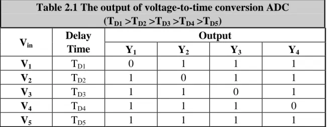
The digital voltage-to-time conversion technique, can be employed as controlled circuit. The basic block and timing diagram of this controlled circuit are shown in Fig2.7. The inverter steps within the gate delay pulse group are P1, P2, P3,..., which are steady states (1,0,1,...). Measurement process starts with the rise of pulse PA, then the P1, P2, P3, ... are going to invert. Due to the propagation delay time, there is an overlap between two 1's or 0's as shown in Fig 2.8. When pulse PB starts to rise, the number of inverters in which its outputs have changed due to PA is equal the
measurement time. Table 2.l illustrates the XOR gate outputs for 4-stage delay line, the 0's output logic means that position of the overlap between two l's logic. This 0's logic will be cached at Yl at level V1 of the input, at Y2 at level V2, and so on, where
D Q PA PB D Q D Q D Q D Q
V
in Y1 Y2 Y3 Y4Figure 2.7 Voltage to time conversion concept using digital circuit.
PA P1 P2 P3 P4 PB TD TS
Figure 2.8 Voltage to time conversion wave signals.
Table 2.1 The output of voltage-to-time conversion ADC
(T
D1>T
D2>T
D3>T
D4>T
D5)
V
inDelay
Time
Output
Y
1Y
2Y
3Y
4V
1T
D10
1
1
1
V
2T
D21
0
1
1
V
3T
D31
1
0
1
2.3 Temperature Sensor Circuit Evolution
In recent years, numerous portable electronic products have been launched to the market with considerable market growth. With process scaling down continuously, this high level of integration also introduces the problem of self-heating, which is the result of increased power density. Low cost, low power, high-performance temperature sensors are therefore becoming increasingly important for applications from power consumption control to thermal monitoring, so as to enhance performance and reliability. The important applications of smart temperature sensors include:
1) The power consumption control in VLSI chips, such as CPU and chip sets. 2) The thermal compensation in single-chip systems and micro systems with built-in sensors.
3) The environment temperature monitors in automatic fabrication factories. 4) The temperature control of consumer electronics, such as automobiles and home
electronics. Kim et al. [2.4] use temperature Sensor for Mobile DRAM Self-refresh Control.
2.3.1 Analog Temperature Sensor
Several different implementations of on-chip temperature sensors have been reported in the last ten years. With the use of bipolar transistors for temperature sensing, and advanced techniques including chopping circuit, dynamic element matching and sigma-delta ADC for noise suppression and cancellation, Pertijs et al. [2.5] developed an on-chip temperature sensor with a 3σ inaccuracy of ±1℃at the expense of increased circuit complexity.
With the use of three CMOS transistors for temperature sensor was presented in [2.6]. The three-transistor temperature sensor shows in Fig. 2.9, which utilizes the
temperature characteristic of the threshold voltage, shows highly linear characteristics at a power supply voltage of 1.8 V. The conditions of this temperature sensor are defined as follows.
1) All transistors operate in the saturation region. 2) The output voltages of each node are equal. 3) The sinking currents at each node are equal.
The temperature is obtained by measuring VOUT, where the two currents, IOUT1 and
IOUT2, have the same value. When the substrate bias effect of the transistor M2 is
neglected to simplify the calculation, their IDS-VGS characteristics and the operating
conditions are 2 1 1 1 1
(
)
2
GS T DSV
V
I
(2.13) 1 1 1 1L
W
C
OX eff
(2.14) 2 2 2 2 2(
)
2
GS T DSV
V
I
(2.15) 2 2 2 2L
W
C
OX eff
(2.16) 2 3 3 3 3(
)
2
GS T DSV
V
I
(2.17) 3 3 3 3L
W
C
OX ef
(2.18) 3 2 1 DS DS DSI
I
I
(2.19)After solving (2.16) - (2.18) for each transistor’s respective VGS, the results are
applied to VGS2and VGS3 in (2.20). Then, IDS2 and IDS3 are also substituted for
(2.13)&(2.14) using (2.19). Finally, (2.21) is solved against VGS1 and we get
T
V
V
V
V
V
OUT GS T T T
)
/
/
(
1
)
/
/
(
3 1 2 1 1 3 1 2 1 3 2 1 1
(2.22)dT
dV
b
dT
dV
dT
dV
a
dT
dV
OUT1 T2 T3 T1)
(
(2.23) Where)
/
/
(
1
1
3 1 2 1
a
)
/
/
(
1
/
/
3 1 2 1 3 1 2 1
b
Since 1/2 1/3 can be assumed as constant, the variables and in (2.23) also become constant. Therefore, the output voltage corresponds to the temperature coefficients of the transistor threshold voltages.
Fig. 2.10 shows the characteristics at 1.8V and 1V supply voltages, where the intersections of and correspond to the operating points of this sensor. This method shows highly linear characteristics at a power supply voltage of 1.8V or more, which enables us to define the operating conditions well above twice the threshold voltage. But the linearity diminishes after scaling down the supply voltage to 1V using a 90-nm CMOS process. Because the temperature coefficient of the operating point’s current at a 1V supply voltage is steeper than the coefficient at a 1.8V supply voltage, the operating point’s current at high temperature becomes quite small and the output voltage goes into the subthreshold region or the cutoff region.
Figure 2.10 Operating-point comparison of three-transistor temperature sensor on IDS-VGS curves at 1.8- and 1.0-V supply voltage.
To improve linearity at a 1V supply voltage, an accurate four-transistor temperature sensor was designed in [2.7] shows in Fig. 2.11, and developed for thermal testing and
Of course, the bias voltage generation circuit must not possess temperature dependency, and, in some cases, this circuit becomes larger than the temperature sensor itself.
In addition, the W/L ratio of the transistors M0 and M1 should be as small as possible so that the current IOUT 1 remains small. However, the smaller W/L ratio
requires a longer channel, so it occupies larger chip area. Consequently, there is a tradeoff between the current consumption and the chip area.
The IDS VGS characteristics and the operating conditions of both the proposed four-transistor sensor is the following:
T
V
I
V
I
V
DS T T DS OUT
3 3 3 2 2 2 12
2
(2.24) 3 3 2 2 2 2 DS DS I Ican be assumed as a constant value. Thus, (2.24) shows that the output voltage is mainly proportional to the temperature characteristics of the threshold voltage (M2 and M3).
The output current of four- transistor temperature sensor is more high linearity with high temperature than conventional three-transistor circuit shows in Fig 2.12.
Figure 2.12 Operating points of four-transistor temperature sensor.
2.3.2 Time-to-Digital Based Temperature Sensors
In the late 20th century, analog-to-digital converters (ADCs) were gradually integrated into analog thermal sensors by IC designers to compose the so-called intelligent or smart temperature sensors. The typical block diagram of the conventional smart temperature sensor is depicted in Fig. 2.13 [2.8]. The sensor consumes more power, and large area, so another version of all-digital temperature sensor which is based on time-to-digital converters instead of ADCs was presented in [2.9]-[2.15].
Figure 2.13 Conventional digital output of temperature sensor.
Figure 2.14 Block diagram of the time-to-digital temperature sensor.
The temperature sensor composed of temperature-to-pulse generator and cyclic time-to-digital converter, shows in Fig 2.14. Temperature-to-pulse generator, it can generate a pulse width is linear to temperature variation. A simple circuit utilizing gate delays to generate the thermally sensitive pulse is shown in Fig. 2.15. The START signal is delayed a certain amount of time by the delay line composed of even number of inverter. The high-to-low and low-to-high propagation delay time for an inverter can be expressed as [2.16]
)
5
.
0
2
5
.
1
ln(
)
(
)
(
2
2 DD TN DD TN DD N L TN DD N TN L PHLV
V
V
V
V
K
C
V
V
K
V
C
t
(2.25))
5
.
0
2
5
.
1
ln(
)
(
)
(
2
2 DD TP DD TP DD P L TP DD P TP L PHLV
V
V
V
V
K
C
V
V
K
V
C
t
(2.26)WherekN NCOX(W/L)N, kP PCOX(W/L)Pand CL are the transconductance
parameters and effective load capacitance of the inverter. Note that we assume square-law behavior for the CMOS devices and thereby ignore the effects of velocity saturation. For an inverter with equivalent NMOS and PMOS, the propagation delay can be derived as
)
5
.
0
2
5
.
1
ln(
)
(
)
/
(
2
DD T DD T DD OX L PHL PLH PV
V
V
V
V
C
C
W
L
t
t
t
(2.27) Where kmT
T
)
(
0 0
,km
1
.
2
~
2
.
0
(2.28))
(
)
(
)
(
T
V
T
0T
T
0V
T
T
,
0
.
5
~
3
.
0
mv
/
k
(2.29) As the temperature increases, the mobility (μ) and the threshold voltage (VT) willboth decrease. In the case of VDD much larger than VT, the thermal effect of the
propagation delay will be dominated by the mobility. That is, the thermal coefficient of the propagation delay will become positive. The major problem of the simple temperature-to-pulse generator is that the width of the output pulse at the lower bound of the measurement range is usually much larger than zero. This will cause a large DC offset at the smart temperature sensor output. The second delay line with thermal compensation for temperature sensitivity reduction is inserted in the lower transmission path of the START signal to reduce the width offset of the output pulse, which is shown in Fig. 2.16. The width offset of the output can be easily reduced by adjusting the number of delay cells in delay line 2.
Figure 2.15 Temperature-to-pulse generator.
Figure 2.16 Width offset reduction accomplished by delay line 2.
As shown in Fig. 2.17, a simple thermal compensation circuit is used to reduce the sensitivity of the inverter in delay line2. The diode connected transistors P1, N1, and P3 serve as the core of the thermal compensation circuit. Since P1, P3, and N1 are all diode connected, they will operate in saturation if bias current is flowing. Thus, we have
Figure 2.17 Delay cell is used in delay line 2.
)
1
(
)
)(
(
2
1
3 2 3 3 OX GSP T GSP DPV
V
V
L
W
C
I
(2.30) By substituting (2.28) and (2.29) into (2.30), the equation becomes
(
)
(
)
(
1
)
)
)(
(
2
1
3 2 0 0 3 0 0 3 GSP T GSP km OX DPV
V
T
T
T
V
T
T
L
W
C
I
(2.31)When the temperature is higher than 200K, a significant plateau effect can be observed for the difference between mask channel length and effective channel length. The thermal sensitivity of channel length modulation term (1VGSP3)will be neglected in the following deviations since it is much smaller than those of mobility and threshold voltage over the temperature range we are interested.
To get the minimum thermal sensitivity, let 3 0
T IDP
(
)
(
)
(
1
)
)
)(
(
)
1
(
)
(
)
(
)
)(
(
2
3 0 0 3 0 0 3 2 0 0 3 1 0 0 0 GSP T GSP km OX GSP T GSP km OXV
T
T
T
V
V
T
T
L
W
C
V
T
T
T
V
V
T
T
L
W
T
km
C
After simplification, we have
km
T
T
T
T
V
V
GSP3
T(
0)
(
0)
2
(2.32)The sizes of transistors P1 and N1 are adjusted to make the gate-to-source voltage of P3 fit the requirement stated in (2.32) as closely as possible. The conduction current of transistor P3 can be found by substituting (2.32) back into (2.31) to yield
)
1
(
2
)
)(
(
2
1
3 2 0 0 3 GSP km OX DPV
km
T
T
T
L
W
C
I
(2.33)Whenkm2, the drain current will become totally thermal independent
)
1
(
)
)(
(
2
1
3 2 0 0 3 OX GSP DPT
V
L
W
C
I
Through the help of the current mirrors (P1, P2) and (N1, N2), the drain current of the inverter will be kept thermally insensitive as well, as will the propagation delay of delay line 2. This greatly reduces the design difficulty and enhances the tolerance to process variation.
Finally, the cyclic time-to-digital converter, shows in Fig 2.18, it convert the pulse width of temperature-to-pulse generator to digital output code.
2.3.3 Dual-DLL-Based All-Digital Temperature Sensors
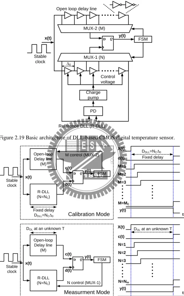
With process scaling down continuously, PVT variation will be a big problem about Time-to-digital based temperature sensors. A new type DLL-based all-digital temperature sensor [2.17] was presented. It has two improvements. First, it removes the effect of process variation on inverter delays via calibration at one temperature point, thus, reducing high volume production cost. Second, we used two fine-precision DLLs, one to synthesize a set of temperature-independent delay references in a closed loop, the other as a TDC to compare temperature-dependent inverter delays to the references. The use of DLLs simplifies sensor operation and yields a high measurement bandwidth (5kS/s) at 7bit resolution, which could enable fast temperature tracking.
We execute calibration and delay normalization using the circuit of Fig. 2.19. It contains an open-loop delay line, and a DLL that synthesizes temperature-independent-delay references. This reference-DLL (R-DLL) is locked to a crystal oscillator x(t): each delay cell in the R-DLL has constant delay Δ0. MUX-1 taps a node in the R-DLL delay line: if the N-th cell’s output is tapped, the delay from input x(t) to output d(t) of the R-DLL is DDLL = NΔ0. This is our delay reference
independent of temperature and process. N can be altered to produce different reference delays. In the open-loop line, if the M-th cell’s output is tapped by MUX-2, the delay between input x(t) and output c(t) is varies with temperature and process.
MUX-2 (M) D Q MUX-1 (N) y(t) FSM Charge pump PD x(t) Stable clock Control voltage Open loop delay line
Reference DLL (R-DLL) ∆0
Figure 2.19 Basic architecture of DLL-based CMOS digital temperature sensor.
D Q y(t) FSM x(t) Stable clock Open-loop Delay line (M) R-DLL (N=NC) c(t) d(t) M control (MUX-2) Fixed delay DDLL=NC∆0 Calibration Mode D Q y(t) FSM x(t) Stable clock Open-loop Delay line (M) R-DLL (N=NC) c(t) d(t) N control (MUX-1) DOL at an unknown T Measurment Mode X(t) d(t) M=1 y(t) M=2 M=3 M=MC t X(t) c(t) N=1 y(t) N=2 N=3 N=Nm t DDLL=NC∆0 Fixed delay DOL at an unknown T
In calibration mode at temperature TC, we set N = NC to fix the reference delay at
DDLL = NCΔ0. We then increase M (MUX-2 setting) until DOL equals DDLL at M = MC.
This comparison of DOL to DDLL to find their lock at M = MC is done via the
bang-bang phase detector in the middle of Fig. 2.19. Then the MC value is
corresponding to process corner.
Once 1-point calibration is complete, the sensor enters measurement mode. Temperature T is unknown, thus, DOL of the hardwired open-loop line is an unknown
delay, which the M-DLL measures by varying the reference delay DDLL of the R-DLL
(bottom of Fig. 2.20). MUX-1 setting N is varied until DDLL equals DOL at N = Nm.
Nm is a digital output that faithfully represents T. Nm corresponds to the normalized delay seen earlier. Fig. 2.21 shows the implemented architecture.
MUX-2 (M) D Q MUX-1 (N) y(t) FSM x(t) Stable clock
Open loop delay line
R-DLL ∆0 D Q Q Control voltage PD Phase interpolator d(t) Phase interpolator c(t)
2.4 PVT Sensors Applications
The important applications of temperature sensors include:
1) The temperature control of consumer electronics, such as automobiles and home electronics.
2) The power consumption control in VLSI chips, such as CPU and chip sets; 3) The environment temperature monitor in automatic fabrication factories; 4) The temperature control of 3D-ICs.
5) The temperature compensation of clock skew in synchronous digital circuit.
2.4.1 CMOS Temperature Sensor with Ring Oscillator for Mobile
DRAM Self-refresh Control
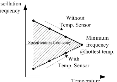
Low-power mobile DRAM can adjust its self-refresh period according to internal temperature to minimize data retention current during power-down mode [2.4]. Usually, the leakage characteristic of a DRAM cell becomes worse at high temperature than at low temperature. Hence, for a conventional DRAM with no self-refresh control scheme, the interval for self-refresh operation must be determined by the hottest temperature condition. This means that data retention current is wasted at low temperature due to too early refresh of memory cells. Moreover, if a local clock signal to determine the self-refresh interval is generated by a ring oscillator as conventional DRAMs do, the wasted data retention current tends to be further increased at low temperature because the oscillation frequency of the oscillator increases as temperature decreases. This situation is described by the upper curve in Fig. 2.22 showing the dependency of the oscillation frequency of a ring oscillator on temperature variation. On the other hand, if we can measure the temperature using a temperature sensor, the self-refresh period can be adjusted adaptively based on this
measured temperature. That is, the period can be set long at low temperature and short at high temperature, as seen by the lower curve in Fig. 2.22
Figure 2.22. The oscillation frequency of ring oscillator with and without temperature-driven control scheme for self-refresh of DRAM
Fig. 2.23 depicts the circuit implementation of the self-refresh control scheme for a mobile DRAM with a temperature sensor.
Figure 2.23. Circuit diagram of DRAM self-refresh control scheme with temperature sensor
2.4.2 Thermally Robust Clocking Schemes for 3D Integrated Circuits
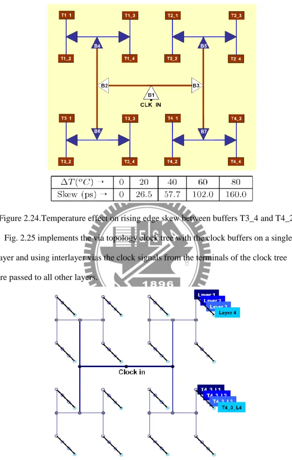
3D integration of multiple active layers into a single chip is a viable technique that greatly reduces the length of global wires by providing vertical connections between layers. However, dissipating the heat generated in the 3D chips possesses a major challenge to the success of the technology and is the subject of active current research. Since the generated heat degrades the performance of the chip, thermally insensitive/adaptive circuit design techniques are required for better overall system performance. A thermally adaptive 3D clocking scheme that dynamically adjusts the driving strengths of the clock buffers to reduce the clock skew between terminals [2.18].
For the synchronous part of a 3D chip, which may be distributed across layers, skewless clock signal is of utmost importance for the accuracy and speed of operation of a design. Since the clock network spans over most parts of the chip and thereby gets exposed to as diverse temperature range as occurs across the chip, the effect of temperature is very pronounced in clock trees. Fig. 2.24 shows an H-tree for a single layer of a 3D chip where we can see that for a number of physically close terminals the clock signals traverse through entirely different temperature zones to reach the terminals which can lead to significant skew between these terminals.
Figure 2.24.Temperature effect on rising edge skew between buffers T3_4 and T4_2. Fig. 2.25 implements the via topology clock tree with the clock buffers on a single layer and using interlayer vias the clock signals from the terminals of the clock tree are passed to all other layers.
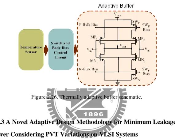
An adaptive circuit scheme was presented to reduce the variation of the clock skew with temperature gradient in the 3D design in Fig. 2.26. The temperature sensors sense the ambient temperatures and convert the temperatures to voltages that are processed by a wave shaping circuitry and finally used for dynamically changing the driving strengths of the clock buffers to reduce the overall skew.
Figure 2.26. Thermally adaptive buffer schematic.
2.4.3 A Novel Adaptive Design Methodology for Minimum Leakage
Power Considering PVT Variations on VLSI Systems
A novel design method to minimize the leakage power during standby mode using a novel adaptive supply voltage and body-bias voltage generating technique for nanoscale VLSI systems [2.19]. The minimum level of VDD and the optimum
body-bias voltage are generated for different temperature and process conditions adaptively using a lookup table method based on the PVT monitoring and controlling systems shows in Fig 2.27. The process, voltage, and temperature (PVT) variations are monitored and controlled independently by their own dedicated systems shows in Fig 2.28. The subthreshold current as well as gate-tunneling and band-to-band-tunneling currents are monitored and minimized adaptively by the
optimally generated body-bias voltage.
(b)
Figure 2.28. (a) Temperature monitoring circuit. (b) Process monitoring circuit.
2.5 Summary
Process, voltage, and temperature variability has become a fundamental challenge in nanometer technologies. This trend is driven by: a) Moore’s law, which governs the exponential growth of transistors in ICs, b) the low-power requirements of mobile devices (i.e., Vdd < 0.5V), and c) the shrinking geometries of advanced CMOS technologies reaching the sub-nanometer dimensions. Therefore, understanding PVT variability is a key to successfully designing ultra-low-power multi-million-gate systems on-a-chip. In this chapter introduces the previous of PVT sensors in power management system. Conventional on-chip PVT sensors that measure PVT variability are described in this chapter.
Chapter 3 Fully On-Chip Process,
Voltage, and Temperature Sensors
The past 20 years have seen enormous growth in the capability and ubiquity of digital integrated circuits. Today, it sometimes seems difficult to buy any product without them—even greeting cards have chips in them. In a short review paper like this, it is unfortunately impossible to mention (let alone describe) all of the great work that was done and published in the VLSI Circuits Symposium during this period. Time-to-Digital-Converter (TDC) is usually used to replace analog circuit. Its applications are gradually expanding such as a phase comparator of all-digital-PLL [3.1], [3.2], PVT sensors circuit [2.9]-[2.14], jitter measurement [3.3], modulation circuit and demodulation circuit as well as a TDC-based ADC [3.4]. The TDC will play more important role in nano-CMOS era because it is well-matched to implement with fine digital CMOS process; it consists of mostly digital circuits and as the switching speed increases, its performance is improved.
However, TDC converters are adopted in [3.5]. As a result, hundreds of inverters were required to obtain enough pulse delay to achieve sufficient temperature resolution. A DLL based temperature sensor has problems of occupying large area, consuming high power. In order to solve these problems, the frequency-to-digital converter (FDC) based smart PVT sensors are proposed in this chapter. The proposed FDC exhibits simple and efficient feature in the process of measuring PVT variation and converting it to digital value. Compared to previous work, the proposed PVT sensors are small-area, low-power, and high performance.
3.1 Time to Digital Converter (TDC) Architecture
A Time-to-Digital-Converter (TDC) is to measure the interval time between two signals, and its time resolution of several pico seconds is achieved when it is implemented with advanced CMOS process. The next will introduce two types of TDC architecture.
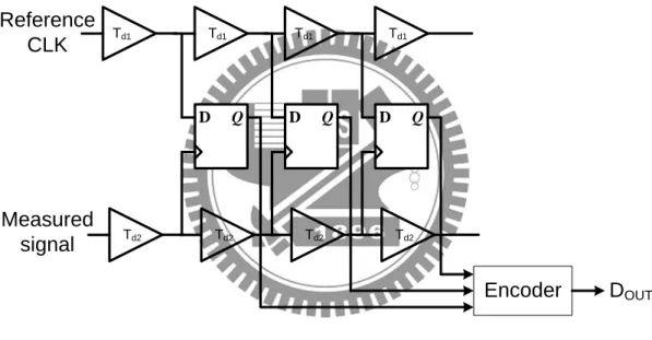
3.1.1 Basic TDC Architecture
Fig. 3.1 shows configuration of a basic TDC, where the reference CLK passes through a buffer line which consists of an inverter chain, and the delayed reference CLK signals are fed into Flip-Flops as their data input. Also the measured signal is fed into Flip-Flops as their clock signal. We obtain the outputs of the Flip-Flops as a thermometer code, according to the rise-edge-timing interval between the reference CLK and the measured signal, and the encoder transforms it into a binary code. Its time resolution is given as the gate delay Td.
Td Td Td Td Reference CLK Measured signal D Q D Q D Q Encoder DOUT
Figure 3.1 A basic TDC architecture.
3.1.2 Vernier Delay Line TDC Architecture
Fig. 3.2 shows a vernier delay line TDC which uses two delay lines: one is for the reference CLK with the buffer delay of Td1. and the other is for the measured signal
with the buffer delay of Td2. Its time resolution is given by Td1− Td2 (gate delay
difference) which can be smaller than the basic TDC, but note that it uses 2N buffers (N buffers of Td1 and N buffers of Td2) for the input range from 0 to N(Td1 − Td2). A
new calibration method for a Vernier-based time-to-digital converter (TDC) was presented [3.6]. The method eliminates the need for accurate external sources typically used for TDC calibration. Simulation and experimental results using a field programmable gate array platform indicate that the method can successfully be employed to calibrate high-resolution TDCs with reasonable accuracy.
Td1 Td1 Td1 Td1 Reference CLK Measured signal D Q D Q D Q Encoder DOUT Td2 Td2 Td2 Td2
Figure 3.2 A vernier delay line TDC.
3.2 Frequency to Digital Converter (FDC)
A TDC based PVT sensors have problems of occupying large area, consuming high power. In this thesis, we propose frequency-to-digital converter (FDC) based PVT sensors with small area, low-power, and high-resolution. Fig. 3.3 shows the proposed frequency-to-digital converter (FDC) exhibits simple and efficient feature in
sensitive oscillator (PVTSO). The PVTSO are constructed from ring oscillators using a current starved delay cell.
.
Fixed Pulse Width
Generator
PVT variations
sensitive
oscillator (PVTSO)
Counter
Digital output
Current starved delay cell
Figure 3.3 Frequency-to-digital converter (FDC) Architecture.
3.3 Fixed Pulse Width Generator
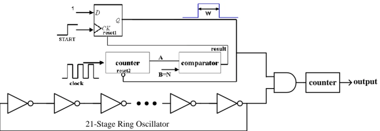
The proposed fixed pulse generator generates a pulse signal width independent of PVT variation. The detail schematic of the fixed pulse generator is drawn in Fig. 3.4. It is composed of D-type flip-flop, counter and comparator. When START signal rises, over a delay time (Td1), the output of D-type flip-flop also rises. When ―result‖ signal rises, over a delay time (Td2), the output of D-type flip-flop will be reset to 0. The delay time Td1 and Td2 both affected by similar PVT variation, so it can be removed. From the above description, the output pulse signal width (W) is invariant from PVT variation. The simulation result of fixed pulse generator shows in Fig. 3.5. The circuit output pulse width is independent of PVT variation.
D
Q
RESETcounter
comparator
V
DDSTART
reset2
result
Clock=10KHzW
N
START
Q
CLK
1 2 3 NW
Td1 Td2 TdcFigure 3.4Fixed pulse generator block diagram and wave form.
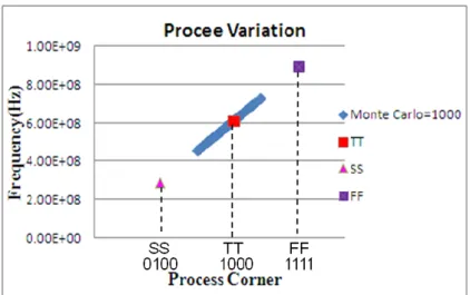
1.00E-07 2.00E-07 3.00E-07 4.00E-07 5.00E-07 6.00E-07 7.00E-07 8.00E-07 9.00E-07 -25 25 75 125 Pul s e _ w idt h (m) Temperature(°C)
Fixed Pulse Generator
VDD=0.3V_TT VDD=0.3V_SS VDD=0.3V_FF VDD=0.4V_TT VDD=0.4V_SS VDD=0.4V_FF