國 立 交 通 大 學
電信工程研究所
博 士 論 文
應用於多頻段與超寬頻通訊之射頻接收
電路設計與分析
Design and Analysis of RF Receiver Circuits
for Multiband and Ultra-Wideband
Communication Applications
研 究 生 :梁清標 Ching-Piao Liang
指導教授 :鍾世忠 Shyh-Jong Chung
應用於多頻段與超寬頻通訊之射頻接收
電路設計與分析
Design and Analysis of RF Receiver Circuits
for Multiband and Ultra-Wideband
Communication Applications
研究生:梁清標
Student:
Ching-Piao
Liang
指導教授:鍾世忠 博士 Advisor:
Dr.
Shyh-Jong
Chung
國立交通大學
電信工程研究所
博士論文
A Dissertation
Submitted to Institute of Communication Engineering
College of Electrical and Computer Engineering
National Chiao Tung University
in Partial Fulfillment of the Requirements
for the Degree of Doctor of Philosophy
in
Communication Engineering
Hsinchu, Taiwan
應用於多頻段與超寬頻通訊之射頻接收電
路設計與分析
研究生:梁清標 指導教授:鍾世忠 博士
國立交通大學
電信工程研究所
摘要
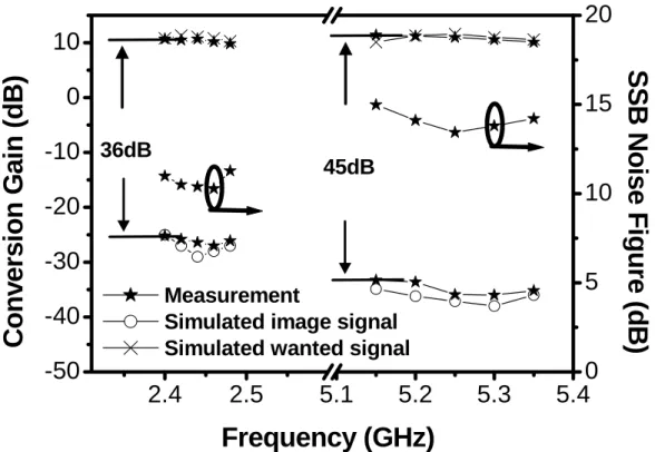
本篇論文提出了數種適用於多頻段與超寬頻通訊系統的 0.18 微米互補式金 氧半製程射頻積體電路元件之架構、分析與設計。其中包含了 (1) 兩個使用諧 振切換與雜訊消除電路的多頻帶低雜訊放大器;(2) 具鏡像頻率抑制混頻器的設計; (3) 三個低功率超寬頻低雜訊放大器的分析與設計;(4) 採用降低相位雜訊技術的壓 控振盪器電路。 多頻帶低雜訊放大器藉由切換的概念來實現多頻帶操作,其能有效地減少系 統面積來降低製作的成本,並且於第二個多頻帶低雜訊放大器設計中,利用回授 式雜訊相消電路能同時達到輸入匹配以及改善雜訊指數的效果。另外在所設計電 路的主動元件中額外引入一阻值較大的基極電阻,以避免雜訊從電晶體的基極端 交互流竄而惡化電路本身的雜訊指數特性。在不額外增加晶片面積、製程步驟、 以及直流功率損耗的前提之下,採用此雜訊降低電阻於2.5 GHz 操作頻帶時,能 達到32%的雜訊指數改善效果,可廣泛地應用在現今低雜訊放大器的設計。 其次,本論文提出了一個具鏡像頻率抑制的吉伯特降頻混頻器。相對於傳統 的Hartley 或 Weaver 鏡像頻率抑制電路架構,此混頻器能大幅地降低直流功率損 耗與電路設計的複雜度。並且搭配一負阻抗產生主動電路,藉由合適的負阻抗來 Q,進而增進鏡像訊號抑制的效果。此混頻器於 2.4/5.2 GHz 使用頻段的量測結果如下:轉換增益 (conversion gain) 為 10.5/11 dB、一階與三階交叉點的輸入功率 (IIP3) 為 4.9/-5.2 dBm、單邊雜訊指 數 (SSB NF) 為 10/13 dB、鏡像頻率抑制效果可達 36/45 dB。 再其次,由於超寬頻系統的訊號強度遠低於IEEE 802.11 a/b/g 以及 1.8 GHz DCS/ GSM 系統,因此首先我們在第一個超寬頻低雜訊放大器中提出具頻帶外訊 號抑制能力的輸入匹配網路去壓制其他系統所造成的干擾。另外我們在第二個低 雜訊放大器電路中,藉由使用一個回授結構以及雙頻帶主動式低功率帶拒濾波電 路進一步地提升抑制干擾訊號的效果。經改良所設計出的低雜訊放大器在 1.8/2.4/5.2 GHz 能夠達到最大抑制效果為 55/48/45 dB。另一方面,由於減少輸入 端損耗元件的使用能有效地改善電路的雜訊指數,在此引入了電晶體的寄生電容 來達到超寬頻輸入匹配特性,當輸入回返損耗 (input return loss) 大於 10 dB 以上 時,其頻帶內最大增益為16.2 dB,最小雜訊指數為 2.3 dB,且總直流功率損耗 僅為6.8 mW。 最後提出的是具降低相位雜訊參數之壓控振盪器電路,藉由最佳化被動元件 尺寸以及額外設計的二次諧波抑制電容與基極偏壓,整體電路性能參數 FOM (figure of merit) 能達到-190 dBc/Hz。此壓控振盪器晶片所使用的面積為 0.15 微 米平方,且由實驗的結果分析得知,總功率耗損僅為1.9 mW,而在 1 MHz offset 時其相位雜訊約為-119 dBc/Hz。
Design and Analysis of RF Receiver Circuits for
Multiband and Ultra-Wideband
Communication Applications
Student:Ching-Piao Liang
Advisor
:
Dr. Shyh-Jong Chung
Department of Communication Engineering
National Chiao Tung University
ABSTRACT
In this dissertation, the design methodologies and implementations of RF receiver circuits for multiband and ultra-wideband communication applications are proposed. There are four parts in this thesis, including: (1) the design of two triple-band low-noise amplifiers (LNAs) using switched resonators and a noise cancelation technique, (2) the design of dual-band image rejection mixer, (3) the analysis and design of three low-power UWB LNAs, and (4) the design of voltage-controlled oscillator (VCO) with phase-noise improvement.
First of all, the design of two triple-band LNAs with switched resonators is presented and fabricated in the TSMC 0.18-μm CMOS process. The proposed triple-band LNAs are demonstrated the feasibility to effectively decrease the size of multi-band RF systems by using a switched component. In addition, a considerable noise power diminution in MOS devices with an additional larger substrate resistor is presented in the second approach of the triple-band LNA. A 32% noise reduction of
MOS devices can be achieved at 2.5 GHz without extra chip area, CMOS process steps and dc power. This noise reduction technique in MOS device is very promising in the nowadays LNA designs.
Secondly, this thesis presents a 2.45/5.2 GHz dual-band Gilbert downconversion mixer with image rejection function is presented, which is implemented in the 0.18-μm CMOS technology. The proposed differential dual-band image rejection circuitry is employed for the 2.45/5.2 GHz WLAN application to effectively diminish the dc power consumption and complexity of circuit design compared to the traditional Hartley or Weaver architectures. Moreover, the cross-connected pair consisted of NMOS and PMOS transistors in the proposed notch filter will further ameliorate the image rejection capability. The IC prototype attains conversion gain of 10.5/11 dB, IIP3 of -4.9/-5.2 dBm for RF= 2.45/5.2 GHz and IF=500 MHz while the image rejection ratio is better than 36/45 dB in the whole operation bandwidth.
Thirdly, three low-power UWB LNAs using 0.18-μm CMOS technology are presented. Due to the FCC’s stringent power-emission limitation at the transmitter, the received signal power in the UWB system is smaller than those of the close narrow-band interferers such as the IEEE 802.11 a/b/g WLAN, and the 1.8 GHz DCS/ GSM. Therefore, we proposed a wideband input network with out-band rejection capability to suppress the out-band interference for our first UWB LNA. Moreover, a feedback structure and dual-band notch filter with low power active inductors will further attenuate the outband interferers without deteriorating the input matching bandwidth in the second UWB LNA. The 55/48/45 dB maximum rejections at 1.8/2.4/5.2 GHz, 15 dB power gain, and 3.5 dB minimum noise figure can be measured while consuming dc power of only 5 mW. On the other hand, to further improve the noise figure performance of the above out-band rejection LNAs, a new
input match network can be obtained easily by selecting an appropriate width of the transistor, which could effectively avoid the usage of the low-Q on-chip inductors in the input network. The IC prototype achieves good performances: 16.2 dB maximum power gain, better than 10 dB input return loss, and 2.3 dB minimum noise figure while consuming dc power of only 6.8 mW.
Finally, a low-power 5.25 GHz VCO with phase-noise improvement is designed in a 0.18-μm CMOS 1P6M process. Due to the usage of a larger value of parallel capacitor, an additional harmonic-suppressed capacitor, and an appropriate bulk bias voltage of the transistor, a good figure of merit (FOM) of -190 dBc/Hz can be achieved without extra chip area and CMOS process steps. The fabricated VCO operates from 5.12 to 5.36 GHz with a power consumption of 1.9 mW and active chip area of 0.15 mm2. The measured phase noise at 1 MHz offset is about -119 dBc/Hz.
誌謝
本論文的完成,有賴許多貴人的協助、支持、鼓勵與相伴,在此衷心的感謝 您們!首先,我要感謝我的指導教授鍾世忠博士,在這四年半的博士班生涯中, 對於研究方面給予細心的指導,不厭其煩的叮嚀以及對我的包容與關懷,無論是 學術研究或待人處世,使學生在學業上獲得許多的知識並找到屬於自己的方向與 目標。此外也要特別感謝碩士班指導教授黃建彰博士,因為老師的栽培提攜,在 研究上給予學生滿滿的熱誠與信心,讓學生能順利的進入交通大學就讀博士班, 並以樂觀的思維來面對博士班的各種挫折與挑戰。 在此感謝口試老師:陳俊雄教授、黃天偉教授、張志揚教授、孟慶宗教授、 郭建男教授、邱煥凱教授,能在百忙之中抽空前來,給予論文上的指導與建議, 讓學生受益良多,也使得論文更為完備。感謝大學時期電子學啟蒙老師林螢光教 授在學生追求學問最無助的時候適時的拉我一把,讓學生能把電子學相關課程的 基礎扎穩,這份恩情學生永遠謹記在心;感謝學長佩宗、侑信與學姐菁偉,在研 究上給予的指導和建議;助理珮華姐姐的關心與協助;助理柯柯老人家所帶來的 歡笑;學弟妹顯鴻、郁娟、敦智、煥能、源哥、竣義、孝聰、泓偉、淑君、天建、 威璁、智偉、明緯、郁凱,在課業上互相的砥礪與生活上的陪伴,慶幸我們能共 同擁有酸苦甘甜的回憶;同時也感謝好友楊翎、鴻依給予的關心與包容,並且總 是能適時的替我分憂解勞;碩班同窗好友德棻、韋廷、煥哲、威弦、菘茂在實作 上提供的寶貴經驗;另外,要特別感謝伯父(曾世忠)與伯母(張素華)在日常生活 上給予實質與心靈上幫忙與鼓勵。 最重要的是感謝我的家人,特別是我的父母,因為有你們無私的奉獻與支 持,讓我無後顧之憂地完成學業與研究,才能成就今日的我。謹以此論文獻給所 有幫助過我與關心我的人。 梁清標 于新竹交大CONTENTS
ABSTRACT (Chinese)
i
ABSTRACT (English)
iii
ACHNOWLEDGEMENT
vi
CONTENTS
vii
TABLE CAPTIONS
ix
FIGURE CAPTIONS
x
CHAPTER 1 INTRODUCTION
1
1.1 BACKGROUND1
1.2 RESEARCH MOTIVATION2
1.3 THESIS ORGANIZATION4
CHAPTER 2 TRIPLE-BAND LOW NOISE AMPLIFIER
7
2.1 INTRODUCTION
7
2.2 TRIPLE-BAND LOW NOISE AMPLIFIER WITHINPUT MATCHING DESIGN
10
2.2.1 Circuit Design and Analysis
10
2.2.2 Simulation and Experimental Results14
2.3 TRIPLE-BAND LOW NOISE AMPLIFIER WITHNOISE REDUCTION
17
2.3.1 Triple-Band Load Network
17
2.3.2 Input Matching with Partial Noise Cancellation19
2.3.3 Noise Reduction with Larger Substrate Resistor22
2.3.4 Simulation and Experimental Results25
2.4 SUMMARY29
CHAPTER 3 IMAGE-REJECTION MIXER FOR
DUAL-BAND OPERATION
31
3.1 INTRODUCTION
31
3.2 CIRCUIT DESIGN33
3.2.1 Effect of Nonlinearity
34
3.2.2 Filter Design with Negative-Resistance Cells
35
3.3 EXPERIMENTAL RESULTS
39
3.4 SUMMARY42
CHAPTER 4 WIDE-BAND LOW NOISE AMPLIFIER
WITH OUT-BAND REJECTION
44
4.1 INTRODUCTION
44
4.2 WIDE-BAND LOW NOISE AMPLIFIER WITHOUT-BAND REJECTION INPUT NETWORK
47
4.2.1 Circuit Design and Analysis
48
4.2.2 Optimum Out-Band Rejection54
4.2.3 Simulation and Experimental Results59
4.3 WIDE-BAND LOW NOISE AMPLIFIER WITHFEEDBACK STRUCTURE AND NOTCH FILTER
63
4.3.1 Effect of Feedback Structure
63
4.3.2 Analysis of Dual-Band Notch Filter65
4.3.3 Design of Low Power Active Inductor68
4.3.4 Simulation and Experimental Results74
4.4 WIDE-BAND LOW NOISE AMPLIFIER WITHA NEW MATCHING TECHNIQUE
77
4.4.1 Circuit Design and Analysis
77
4.4.2 Simulation and Experimental Results84
4.5 SUMMARY86
CHAPTER 5 VOLTAGE-CONTROLLED OSCILLATOR
WITH PHASE-NOISE IMPROVEMENT
88
5.1 INTRODUCTION88
5.2 CIRCUIT DESIGN90
5.3 EXPERIMENTAL RESULTS94
5.4 SUMMARY97
CHAPTER 6 CONCLUSIONS
99
APPENDIX
101
REFERENCES
102
VITA
109
PUBLICATION LIST
110
TABLE CAPTIONS
Table 2.1
Performance summary of previously published LNAs
30
Table 3.1
Comparison with previously published mixers
43
Table 4.1
UWB LNA Performance summary
87
FIGURE CAPTIONS
Fig. 1.1
Several different applications merged into a system.
3
Fig. 2.1
(a) Triple-band LNA reported in [8], [9]. (b) A
noise-canceling amplifier in [15]-[17].
8
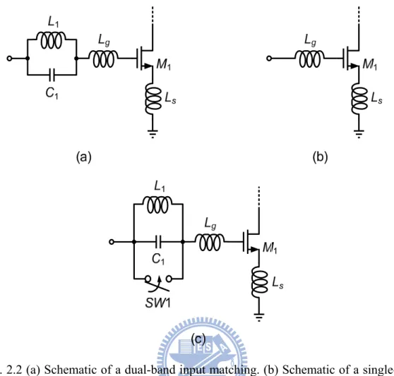
Fig. 2.2
(a) Schematic of a dual-band input matching. (b)
Schematic of a single-band input matching. (c) A
proposed triple-band input matching with an additional
switched component.
11
Fig. 2.3
Complete schematic of the proposed first triple-band
LNA with input matching design.
13
Fig. 2.4
Microphotograph of the first triple-band LNA with
0.98
×0.94 mm
2die area.
14
Fig. 2.5
Measured and simulated S-parameters of proposed
first triple-band LNA.
15
Fig. 2.6
Measured and simulated noise figure of proposed first
triple-band LNA.
16
Fig. 2.7
(a) Schematic of a dual-band load network. (b)
Schematic of a single-band load network. (c) A
proposed triple-band load network with an additional
switched component.
18
Fig. 2.8
The load impedance versus frequency with different C
parameters. (a) A dual-band load network when the
switch is on. (b) A single-band load network when the
switch is off.
20
Fig. 2.9
Principle of the noise-canceling technique.
21
Fig. 2.10
Simulated noise figures with and without the
noise-canceling technique.
21
Fig. 2.11
(a) A NMOS device with a larger substrate resistance
R
B=8 kΩ. (b) Structure of a NMOS with a larger
substrate resistance R
B. (c) The noise equivalent circuit
of NMOS device with a larger substrate resistance R
B.
23
Fig. 2.12
Simulated the total MOS device noise factor F
(NF=10log
10F) with and without the additional
resistance R
B=8 kΩ and the noise reduction when
resistance R
Bis used.
24
Fig. 2.13
Simulated noise figure with and without the additional
resistor R
=8 kΩ. (a) Dual-band status when the
switch is on. (b) Single-band status when the switch is
off.
Fig.
2.14 Complete schematic of the proposed second
triple-band LNA with the load network design and the
noise reduction resistance R
B.
26
Fig. 2.15
Microphotograph of the second triple-band LNA with
0.75
×0.69 mm
2die area.
27
Fig. 2.16
Measured and simulated S-parameters of the second
triple-band LNA.
28
Fig. 2.17
Measured and simulated noise figure of the second
triple-band LNA.
28
Fig. 3.1
Block diagram of the Hartley down-converter.
32
Fig. 3.2
Block diagram of the Weaver down-converter.
32
Fig. 3.3
Complete schematics of the proposed dual-band image
rejection mixer.
33
Fig. 3.4
The nonlinear effect of a transistor with the bias
voltage V
G1.
34
Fig. 3.5
A third-order notch filter reported in [37].
35
Fig. 3.6
(a) The proposed differential dual-band third-order
notch filter. (b) The half circuit of (a). (c) Equivalent
circuit at low frequency. (d) Equivalent circuit at high
frequency.
36
Fig. 3.7
The proposed differential dual-band notch filter with
the negative-resistance cells consisted of NMOS and
PMOS transistors.
38
Fig. 3.8
The proposed notch filter in the dual-band operation
frequencies has no influence on the impedance
between nodes X and Y.
39
Fig. 3.9
Measured and simulated RF return loss of the
proposed mixer.
40
Fig. 3.10
Conversion gain and noise figure of the proposed
mixer.
41
Fig. 3.11
Measured results of fundamental output power and
IM3 for the proposed mixer with RF input frequency
spacing of 10 MHz.
41
Fig. 3.12
Microphotograph of the mixer. Die area is 1.07
×1.07
mm
2.
Fig. 4.1
Spectrum of the UWB system with large interferers.
45
Fig. 4.2
Complete schematics of the first UWB LNA with
out-band rejection.
48
Fig. 4.3
Simulated ideal power gain with and without out-band
rejection improvement.
50
Fig. 4.4
Input reflection coefficients on the Smith chart for (a)
the L
1C
1-C
RLcircuit with impedance Z
R, (b) the
narrow-band input network with impedance Z
in’, and
(c) the total circuit with impedance Z
in.
52
Fig. 4.5
Equivalent circuits for the broad-band input network at
(a) the parallel resonance frequency ω
1and (b) the
parallel resonance frequency ω
2.
53
Fig. 4.6
(a) Simulated power gain (S
21) and (b) input return loss
(1/S
11) for different values of L
gwith L
1= 2.0 nH, C
1=
0.82 pF, and C
RL= 2.95 pF. The transmission zero
ω
RHis kept constant.
55
Fig. 4.7
The impedance Z
Rversus frequency with different
values of L
1. The transmission zero ω
RLis kept
constant.
57
Fig. 4.8
(a) Simulated power gain (S
21) and (b) input return loss
(1/S
11) for different values of L
1with L
g= 2.0 nH, L
s=
0.5 nH, C
RH= 0.17 pF, and C
a= 0.23 pF. The
transmission zero ω
RLis kept constant.
58
Fig. 4.9
Simulated noise figure of the first UWB LNA due to
the active gain stages and the losses of the input
network.
59
Fig. 4.10
Microphotograph of the fabricated UWB LNA. Die
area is 0.78
×0.8 mm
2.
60
Fig. 4.11
Measured and simulated power gain (S
21) and input
return loss (1/S
11) of the UWB LNA.
61
Fig. 4.12
Measured and simulated noise figure of the UWB
LNA.
61
Fig. 4.13
Measured and simulated IP
1dBand IIP3 of the UWB
LNA.
62
Fig. 4.14
Principle of the interferer-canceling technique with a
feedback capacitor C
FBand active dual-band notch
filter.
64
additional
capacitor
C
FB.
Fig. 4.16
The dual-band notch filter circuit.
66
Fig. 4.17
Simulated transmission coefficient S
21of the notch
filter for different values of L
3.
67
Fig. 4.18
Simulated transmission coefficient S
21of the notch
filter for different values of Q with L
3= 5 nH.
67
Fig. 4.19
(a) Schematic and (b) equivalent circuit of the active
inductor with a resistor in the feedback path.
69
Fig. 4.20
Complete schematics of the proposed second UWB
LNA.
70
Fig. 4.21
Simulated quality factor of the proposed active
inductors L
3and L
4.
71
Fig. 4.22
Inductance of an active inductor is related to the bias
voltages of the transistors.
72
Fig. 4.23
Adjustable quality factor Q of an active inductor while
maintaining a similar inductance value.
73
Fig. 4.24
Principle of the feedback technique for setting the
notch frequency.
73
Fig. 4.25
Microphotograph of the fabricated UWB LNA. Die
area is 0.9
×0.85 mm
2.
74
Fig. 4.26
Measured and simulated power gain (S
21) and input
return loss (1/S
11) of the second UWB LNA.
75
Fig. 4.27
Measured and simulated noise figure of the second
UWB LNA.
75
Fig. 4.28
Bandwidth enhancement techniques (a) the
common-source stages with inductive loads and (b) the
basic principle with inter-stage series resonators.
78
Fig. 4.29
The proposed input matching circuit and its frequency
behavior.
79
Fig. 4.30
The capacitor C
ais substituted for the amplifier stage
M
2with power consumption fixed at 1.5 mW.
80
Fig. 4.31
Simulated input return loss for different widths of the
transistor M
2.
80
Fig. 4.32
Simulated noise figure for different widths of the
transistor M
2.
81
Fig. 4.33
Inter-stage matching network.
82
Fig. 4.34
Input reflection coefficients on the Smith chart for the
impedances Z
1(solid line) and Z
2(dashed line) shown
in Fig. 4.33.
Fig. 4.35
Simulated power gain with and without the inter-stage
matching network.
83
Fig. 4.36
Simulated noise figure for different values of the
resistor R
B.
83
Fig. 4.37
The architecture of the proposed UWB LNA with a
new input-matching technique.
84
Fig. 4.38
Microphotograph of the LNA. Die area is 0.81
×0.81
mm
2.
85
Fig. 4.39
Measured S-parameters of the proposed UWB LNA.
85
Fig. 4.40
Measured noise figure of the proposed UWB LNA.
86
Fig. 5.1
The phase-noise suppression with the second harmonic
tuned LC tank [67].
89
Fig. 5.2
Process steps of the backside ICP deep trench etching
technology [68].
89
Fig. 5.3
Complete schematics of the proposed low-power VCO
with the phase-noise reduction techniques.
90
Fig. 5.4
The equivalent circuits of the proposed VCO when the
voltage at node V
+is (a) high and (b) low.
91
Fig. 5.5
Simulated V
+voltage swing for different values of
C
1.
92
Fig. 5.6
Influence of the capacitor C
Tfor (a) the fundamental
signal and (b) the second harmonic signal.
93
Fig. 5.7
Measured output signals with and without the
capacitor C
T.
93
Fig. 5.8
Simulated phase noises
with and without
improvement.
95
Fig. 5.9
Microphotograph of the VCO with 0.33
×0.45 mm
2core die area.
95
Fig. 5.10
Measured and simulated tuning ranges of the proposed
VCO.
96
Fig. 5.11
Measured and simulated phase noises of the proposed
VCO.
CHAPTER 1
INTRODUCTION
1.1 BACKGROUND
The wireless communication is becoming more and more significant because of the convenience for human-being life and accelerating the transmission of the information in the last two decades. For the landscape of the wireless communication systems, the higher bandwidth of these radio bands, such as wireless local area network (WLAN), worldwide interoperability for microwave access, and ultra-wideband (UWB) significantly enables the higher data rate applications.
The IEEE 802.11 group which is also labeled as WiFi (Wireless Fidelity) establishes three sub-standardsonthe market, namely 802.11aoperating at frequencies allocated around 5 GHz, and 802.11 b and g transmitting at 2.4 GHz. The b standard achieves a date throughput of around 11 Mb/s, and the more advanced a and g standards can support up to 54 Mb/s data rate by utilizing the orthogonal frequency-division multiplexing (OFDM) technique.
Worldwide interoperability for microwave access (WiMAX), described and specified in the IEEE 802.16e standard, is a new system for wireless broadband access to provide the high speed of service and broad coverage of about several miles. Due to the usage of the OFDM technique and the multiple-input, multiple-output (MIMO) concept, the data rate up to 75 Mb/s can be achieved at the operation frequencies 2.5, 3.5, and 5.2 GHz.
For the IEEE 802.15.3a group, the multi-band orthogonal frequency division multiplexing (MB-OFDM) UWB system uses the unlicensed UWB spectrum from 3.1
GHz to 10.6 GHz with a regulated frequency-power emission below −41.3 dBm to provide data communication capabilities up to 480 Mbps. The 7.5 GHz bandwidth is divided into 4 groups of 14 bands. Therefore, the occupied spectrum for each OFDM signal is 528 MHz.
In this thesis, the main research focus is on key components for multiband and UWB communication systems. It includes triple-band low-noise amplifiers (LNAs), a dual-band image rejection mixer, low-power UWB LNAs with out-band rejection properties, and a low phase-noise voltage-controlled oscillator (VCO). The research motivation will be depicted in the following subsection.
1.2 RESEARCH MOTIVATION
Recently, the wireless communication systems has rapidly expanded the demand for low-cost and low-power RF integrated circuits (RFICs) which can support multi-system operations. There is the trend to merge several applications into one device by reusing potential synergies between the different systems, as shown in Fig. 1.1. The study on exploring new different circuit topologies and design techniques of the key RFIC components in multi-band and UWB communication systems is proposed.
For the multi-band communication system, conventional design strategies have adopted different single-band receiver circuits in parallel for different frequency bands. However, it is unavoidable to result in a high implementation cost because of the large chip areaand an increased chip current dissipation simultaneously. In order to avoid the above-mentioned drawbacks, a multi-band receiver has demonstrated the feasibility to take the place of the conventional structure for multi-band
Fig. 1.1 Several different applications merged into a system.
application. In addition, the noise figure of a receiver is particularly determined by the noise figure of the LNA located in front of the receiver. Therefore, the proposed noise-canceling technique can be applied in the LNA circuit to ameliorate the noise property.
Mixer is responsible for frequency conversion in RF transceiver, and the suppression of the image signal is an essential requisite. Generally, the multi-band image rejection mixer can be achieved by either Hartley or Weaver architecture, but the required multi-band quadrature signal generator will further increase the complication of the circuit implementation, which is undesired for low-cost and low-power application. In order to achieve smaller chip area and dc power consumption, the differential third-order notch filter with the cross-connected pair consisted of NMOS and PMOS transistors is designed.
67 dB, in the worst case, lower than those of the WLAN interferer powers at 5.2 and 2.4 GHz, respectively. In addition, one tone is measured at 1.87 GHz in a smart-phone currently on the market, and the power level is 35 dB higher than the UWB signal. All of these interferers have a harmful effect on the received UWB signal; therefore, the designed LNA with out-band rejection property in UWB communication system is required.
For multiband or UWB communication applications, the RF signal is downconverted to the IF frequency using a local oscillator, which is generated by a frequency synthesizer. Phase noise is one of the most critical parameters for a local oscillator since it affects the overall performance of the communication system. Therefore, the designed low-noise VCO, which is a key component of the frequency synthesizer is proposed to optimize the phase-noise performance.
The aim of this dissertation is to develop key components for multiband and UWB communication systems including two triple-band LNAs, a dual-band image rejection mixer, three low-power UWB LNAs, and a low phase-noise VCO. The main results will be depicted below.
1.3 THESIS ORGANIZATION
It is the aim of this thesis to analyze and design RF receiver circuits for multiband and UWB communication applications. The thesis includes the design of two triple-band LNAs, a dual-band image rejection mixer, three low-power UWB LNAs, and a VCO with the phase-noise improvement.
Chapter 1 introduces the background, and describes the research motivation. Chapter 2 presents the design of two triple-band LNAs fabricatedina0.18-μm
complementary metal oxide semiconductor (CMOS) process. The proposed triple-band LNAs have demonstrated the feasibility to effectively decrease the size of multi-band RF systems by using a switched component. Furthermore, the feedback structure is adopted to accomplish the partial noise cancelation and the wideband input matching simultaneously. The proposed noise power diminution by using an additional larger substrate resistor in MOS device can be employed in the nowadays LNA designs.
A 2.45/5.2 GHz Gilbert downconversion mixer with image rejection function is proposed and detailed in chapter 3. The mixer employs the differential, dual-band, third-order notch filter to attenuate the dual-band image signal while maintaininga superior in-band performance. The cross-connected pair consisted of NMOS and PMOS transistors in the proposed notch filter will further raise the Q value of on-chip inductor for improving the image rejection capability.
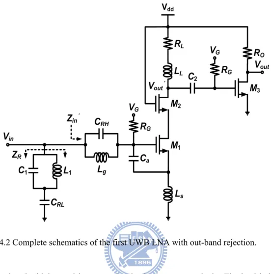
In chapter 4, three low-power UWB LNAs using 0.18-μm CMOS technology are presented. By suitably introducing two additionalcapacitorsinthe traditional LC input network, two transmission zeros are generated to achieve the out-band rejection function. Moreover, a feedback structure and dual-band notch filter with low power active inductors further attenuate the out-band interferers without deteriorating the input matching bandwidth. After improving the out-band rejection capability, a new matching technique can be acquired easily by selecting an appropriate width of the transistor, which will effectively avoid the usage of the low-Q on-chip inductors in the input network for ameliorating the noise figure performance.
In chapter 5, a low-power VCO with phase-noise improvement in 0.18-μm CMOS technology is presented. The VCO adopts the design of a current-reused configuration because of its excellent low-power characteristic, and focuses on the promotion of phase noise without additional chip area and CMOS process steps. A 15
dB improvement at 10 kHz offset frequency can be attained due to the usage of a larger parallel capacitor, an extra harmonic-rejected capacitor, and an appropriate bulk bias voltage of transistor.
CHAPTER 2
DESIGN OF THE TRIPLE-BAND LOW NOISE
AMPLIFIER
2.1 INTRODUCTION
Recently, the widely used wireless communication systems have rapidly expanded the demand for low-cost and low-power RF integrated circuits which can support multi-band operations by a single system. Conventional design strategies have adopted different single-band transceiver circuits in parallel for different frequency bands [1]-[3]; however, it is unavoidable to result in a high implementation cost because of the large chip area, and simultaneously increase chip current dissipation. In order to improve the above-mentioned drawbacks, the topologies of the wideband LNA such as the resistive shunt-feedback structure [4], LC input network [5], common-gate 1/gm termination [6], and the distributed configuration [7] have been demonstrated and designed for multi-band application. Unfortunately, the broadband gain response will cause the unwanted interferers to impair the linearity of the receiver which is not desirable for the system considerations. To avoid this, the triple-band LNA shown in Fig. 2.1(a) has been devised in [8], [9], and it can suppress the out-band interferers while maintaining a sufficient in-band property. Nevertheless, the major drawback is the required high fabrication cost due to the usage of too many inductors. As a consequence, we propose two approaches by using a switched component to reduce the usage of inductors and the significant die area reduction will effectively decrease the cost of a multi-band RF system.
Lg Ls M1 Cg2 Lg2 Cg1 Lg1 Cg3 VG1 RG Vin L2 Cp M3 Cc VG3 RG M2 VG2 Cd2 Ld2 Ld1 Cd1 C12 Ld Vout Cb1 VDD (a) (b)
Fig. 2.1 (a) Triple-band LNA reported in [8], [9]. (b) A noise-canceling amplifier in [15]-[17].
In addition, it has become feasible to improve the noise performance of the LNA using the noise-canceling techniques. A source-degenerated cascode amplifier with an additional inductor at the drain of the main transistor is attractive for its excellent noise
achieved [10]. This is because the noise contribution from the cascode transistor can be reduced by using the inductor to cancel the effect of the parasitic capacitance at the drain of the main transistor. Inevitably, the extra inductor will occupy additional chip area, which makes it undesired for many applications. Inductively coupled plasma (ICP) deep-trench technique, which selectively removes the silicon underneath the inductors, is utilized to ameliorate the quality factor of on-chip inductors [13], [14]. A 0.5 dB noise figure decrease (from 2.28 to 1.78 dB) can be accomplished [13]; nevertheless, the extra CMOS process steps will increase the complication of the circuit implementation. Recently, a feedforward noise-canceling technique shown in Fig. 2.1(b) has been reported in [15]-[17]. The design principle of noise canceling is that the thermal noise of the common-gate amplifier can be neutralized by the voltage-sensing stage; however, the required common-source stage will make the total dc power consumption larger.
In this chapter, a momentous noise power diminution in MOS devices with an additional larger substrate resistor which can be employed in the nowadays LNA designs is presented and demonstrated. It can be observed that a maximum 32% noise reduction can be achieved due to the usage of larger resistance RB without extra chip
area, dc power and CMOS process steps.
This chapter is organized as follows. Section 2.2 introduces the principle of the proposed first triple-band LNA. Section 2.3 describes the detailed analyses of the second triple-band LNA. This chapter is summarized in Section 2.4. The target frequencies of the proposed triple-band LNAs are 2.5, 3.5, and 5.2 GHz, which can be used in the WiMAX system.
2.2 TRIPLE-BAND LOW NOISE AMPLIFIER WITH
INPUT MATCHING DESIGN
It is known that the noise performance of LNA is dominated to the input stage. The proposed first triple-band LNA adopts a source-degenerated cascode amplifier, which selects the appropriate transistor size with finger width fixed at 5 μm to achieve input match and good noise figure simultaneously [18], [19]. Traditionally, the design criteria of the multi-band LNAsuch as that in the WiMAX application have used different LNAs for different frequency bands. Recently, a concept of triple-band LNA, as shown in Fig. 2.1(a), has been proposed [8], [9]. However, the chip area may be consumed while there are eight required inductors in the circuit.
2.2.1 Circuit Design and Analysis
Fig. 2.2(a) and (b) show the conventional dual-band and single-band input matching circuits, respectively. In this section, we have developed a novel manner for triple-band input matching, which is contrived by using dual-band input network with an additional switched component shown in Fig. 2.2(c). A significant area reduction and better noise figure can be achieved by reducing the usage of inductors in the input network. In the following analyses, it will facilitate the discussions to define that ω1, ω2, and ω3 correspond to 2.5, 5.2, and 3.5 GHz, respectively. When the switch is off, the circuit is equivalent to that shown in Fig. 2.2(a), and it is to be operated as a dual-band input network at 2.5 GHz and 5.2 GHz. On the other hand, as the switch is on, the circuit becomes that in Fig. 2.2(b), and it is operated at 3.5 GHz. To this end,
Fig. 2.2 (a) Schematic of a dual-band input matching. (b) Schematic of a single-band input matching. (c) A proposed triple-band input matching with an additional switched component.
circuit should be suitably designed in order to achieve the triple-band input matching. Based on the small-signal analysis, the input impedance for switch off status (Fig. 2.2 (a)) can be expressed as
1 2 1 1
1
(
)
.
1
m s in s g gs gsg L
j L
Z
j
L
L
L C
j C
C
ω
ω
ω
ω
=
+
+
+
+
−
(2.1)To match the input port’s impedance, the real term should be equal to 50 Ω and its imaginary term to zero, which yields
1 1
50
m gs sg
C
L
=
(2.2) and 4 1 2 1 1 1 1 1 1 ( g s) ( g s 1) 0 , gs gs L L C C L L L C C Lω
+ω
+ − + + + = (2.3)As can be seen in (2.3), the designed frequencies ω1 and ω2 (i.e., 2.5 and 5.2 GHz) satisfies 2 2 1 2 1 1 1
1
(
g s)
gsC L
L C L
ω ω
=
+
(2.4) and 1 1 1 2 2 1 2 1 1 . ( ) g s gs g s L L C L C C L L ω ω + + + + = + (2.5) From (2.4), L1 is obtained as 1 2 2 1 2 1 1 1 , ( g s) gs L C L L C
ω ω
= + (2.6)which, upon substitution in (2.5), yields
1 1 ( )( 2 2) ( )2 2 2 2 1 . gs C C L L ω ω C L L ω ω C = + + − + − (2.7)
Fig. 2.3 Complete schematic of the proposed first triple-band LNA with input matching design.
On the other hand, when the switch is on (i.e., the single-band state for ω3=3.5 GHz, Fig. 2.2 (b)), the criterion of a 50 Ω input impedance is still required and Lg can
be expressed as 1 2 2 3 1 3 1 1 50 1 1 , gs g s gs gs m C L L C C g ω ω = − = − (2.8)
where (2.2) has been incorporated. As we will see, the precise values of Ls=0.25 nH,
Lg=3.5 nH, L1=2 nH, and C1=0.9 pF can be predicted by drawing on(2.2),(2.8),(2.7),
and (2.6) when the width of the transistor M1 (300 μm) is chosen with 10 mW power dissipation. The first triple-band LNA is shown in Fig. 2.3 and it is noticed that the equivalent circuit of a switched component exists parasitic capacitances, which cause
Fig. 2.4 Microphotograph of the first triple-band LNA with 0.98×0.94 mm2 die area.
C1 should be adjusted. In addition, for testing purposes, an output buffer consisted of a source follower is included in the design circuit, which roughly introduces a 6 dB loss in the signal path [20].
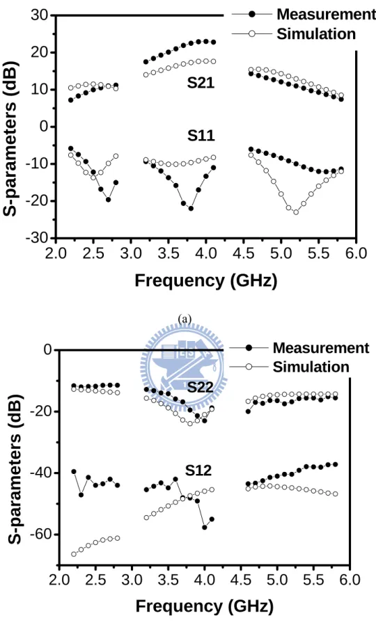
2.2.2 Simulation and Experimental Results
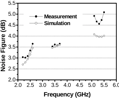
Thediemicrophotograph of the first triple-band LNA is shown in Fig. 2.4, and measured by using on-wafer probing. The LNA chip without the output buffer draws a total 5.5 mA dc current from the 1.8 V supply voltage. The S-parameters of the designed LNA is measured using the Agilent 8510C vector network analyzer. The simulated and measured results of S- parameters are depicted in Fig. 2.5. The measured peak gains are 10/20.1/11 dB at 2.5/3.5/5.2 GHz while the input and output return losses are better than 10 dB in the operation frequencies. The noise figure is measured using the Agilent N8975A noise figure analyzer with Agilent 346C noise source. The simulated and measured noise figures at the same bias condition are depicted in Fig. 2.6. It is seen that the minimum values of the measured noise figure
2.0
2.5
3.0
3.5
4.0
4.5
5.0
5.5
6.0
-30
-20
-10
0
10
20
30
S11
S21
Measurement
Simulation
S-parameters (dB)
Frequency (GHz)
(a)2.0
2.5
3.0
3.5
4.0
4.5
5.0
5.5
6.0
-60
-40
-20
0
S12
S22
Measurement
Simulation
S-parameters (dB)
Frequency (GHz)
(b)2.0 2.5 3.0 3.5 4.0 4.5 5.0 5.5 6.0
2.0
2.5
3.0
3.5
4.0
4.5
5.0
5.5
Measurement
Simulation
Noise Figure (dB)
Frequency (GHz)
2.3 TRIPLE-BAND LOW NOISE AMPLIFIER WITH
NOISE REDUCTION
The first triple-band LNA can reduce chip area significantly by using dual-band input network with an additional switched component. However, it is unavoidable to worse noise figure result due to the usage of low-Q inductors in input network. To enhance the noise performance,we have tried the second LNA which utilizes the double-peak single-notch network [21] with an additional switch as the load impedance to achieve the same characteristic of the first LNA. Moreover, a common-drain stage in the feedback path is adopted to accomplish 50-Ω wideband input matching and partial noise cancellation simultaneously. The buffer transistor with a purely 50-Ω resistive load is employed to achieve output matching for testing purposes.
2.3.1 Triple-Band Load Network
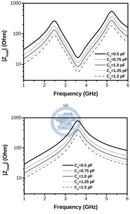
The triple-band load network, as shown in Fig. 2.7(c), is operated by turning the switch MSW1 on and off. Evidently, this network is simplified into a LC tank operated
in ω3=3.5 GHz when the switch MSW1 is off (i.e., Fig. 2.7(b)). Similarly, when the
switch MSW1 is on, the dual-band load impedance operated in ω1=2.5 GHz and ω2=5.2
GHz is employed and expressed by
2 1 1 4 2 1 1 1 1 1 (1 ) . ( ) 1 d load d d d d d j L L C Z L C L C L C L C L C ω ω ω ω − = + + + + (2.9)
Fig. 2.7 (a) Schematic of a dual-band load network. (b) Schematic of a single-band load network. (c) A proposed triple-band load network with an additional switched component.
Equation (2.9) also represents that the two poles ω1 and ω2 can be obtained by letting the denominator equal null, or
4 2
1 1
(
1 1 1) 1 0 .
d d d d d
L C L C
L C
L C
L C
ω
+
ω
+
+
+ =
(2.10)In addition, 1/ LC1 1=1/ L Cd d is satisfied to facilitate the design, which retains to provide similar amplitudes and symmetries in the two maxima of Zload. It is noted that
load components, which means that there is still one degree of freedom, let say Cd,
left for the circuit design. Fig. 2.8(a) and (b) show the load impedance versus frequency with different Cd parameters. In general, the first step in the design criteria
of the proposed load network is to select a lower Cd since the higher the load
impedance, i.e., the LNA gain. However, a drawback which may make the design criteria unsatisfactory is a high implementation cost due to the requirement of the larger inductance L1 and Ld. Therefore, it should be taken into account the trade-off
between the gain and die area punctiliously.
2.3.2 Input Matching with Partial Noise Cancellation
The design of the first stage is a common-source structure with a feedback common-drain amplifier in order to achieve the wideband input matching of 50-Ω. The input impedance Zin shown in Fig. 2.9 is close to 1/gm3(1+ gm1ZL), which is
interrelated to the bias voltage of the transistors M1 and M3 since gmi is proportional to
the current of transistors. Consequently, the input matching characteristic can be effectively tuned by adjusting the bias voltages Vg2, Vg3, and the bias current I4 to
compensate for the process variation. On the other hand, the introducing of a feedback structure with the common-drain stage also can attain the partial noise cancellation, which is demonstrated in the following analyses. As shown in Fig. 2.9, the noise voltage VnX at node X is generated due to the thermal noise current in of the transistor
M1. The adopted feedback common-drain amplifier M3 will bring about the in-phase noise voltage VnYat node Y, which can be further converted to node X with opposite
phase (i.e., the noise voltage VnYX) by the common-source cascode amplifier M1–M2.
Therefore, the noise contributed by M1 is partially cancelled at the output node X, as can be observed from Fig. 2.10.
1
2
3
4
5
6
10
100
1000
|Z
lo a d| (O
h
m
)
Frequency (GHz)
C d=0.5 pF C d=0.75 pF Cd=1.0 pF C d=1.25 pF C d=1.5 pF (a) 1 2 3 4 5 6 10 100 1000 Cd=0.5 pF Cd=0.75 pF Cd=1.0 pF Cd=1.25 pF Cd=1.5 pF|Z
lo ad| (O
h
m
)
Frequency (GHz)
(b)Fig. 2.8 The load impedance versus frequency with different C parameters. (a) A dual-band load network when the switch is on. (b) A single-band load network when
Fig. 2.9 Principle of the noise-canceling technique.
2.0
2.5
3.0
3.5
4.0
4.5
5.0
5.5
2.0
2.5
3.0
3.5
Without Feedback Path
With Feedback Path
NF
mi
n
(dB)
Frequency (GHz)
2.3.3 Noise Reduction with Larger Substrate Resistor
In order to further ameliorate the noise performance of a CMOS LNA, a significant noise power reduction in MOS device by using larger substrate resistor RB,
as shown in Fig. 2.11(a), is presented. To begin with, the complete noise equivalent circuit must be established to facilitate the demonstration of the proposed noise-reduction structure. It is well-known that the body effect transconductance can be expressed as 2 2 mb m f SB g g V
γ
ϕ
= + (2.11)whereγis the body-effect coefficient, φf is the bulk fermi potential, VSB is the voltage
between body and source. If we make the assumption that the source voltage drops sufficiently below the bulk voltage, then it is observed intuitively from Fig. 2.11(b) that the current IB is formed because of the forward-biasing. Contradictorily, the
current IB injected into the external substrate resistance RB will bring about VSB >0.
As a consequence, no current flows between body and source (i.e., VSB=0) and this
means that the body effect transconductance is inexistent in the noise equivalent circuit (see Fig. 2.11(c)) for the MOS device with a larger substrate resistor RB.
Furthermore, the dominant noise source modeled as a shunt current source in the output circuit of the device is channel thermal and the output noise power density arising from this source is
2 2 0
4
'
|
out|
out d di
i
kT g
i
γ
=
(2.12)Fig. 2.11 (a) A NMOSdevice with a larger substrate resistanceRB=8 kΩ. (b) Structure
of a NMOS with a larger substrate resistance RB. (c) The noise equivalent circuit of a
NMOS device with a larger substrate resistance RB.
whereγ’ is a bias-dependent factor, and gd0 is the zero-bias drain conductance of the
device [22, Chapter 7]. In general, 1/sCsb >>Rsb is satisfied and demonstrated in [23];
therefore, the substrate impedance Zsub can be simplified to a simple series CR circuit
(i.e., Cdb in series with (Rdsb+Rsb)||Rdb, and RB) as follows:
( ) 1 . db sb dsb sub B db db sb dsb R R R Z R j C
ω
R R R ⎡ + ⎤ ≈ +⎢ + ⎥ + + ⎣ ⎦ (2.13)1
2
3
4
5
6
0.4
0.5
0.6
0.7
0.8
0.9
1.0
without R
Bwith R
BFrequency (GHz)
Noise factor
20
25
30
35
Noise reduction (%)
Fig. 2.12 Simulated the total MOS device noise factor F (NF=10log10 F) with and without the additional resistance RB=8 kΩ and the noise reduction when resistance RB
is used.
1
2
3
4
5
6
2
3
4
5
0.64dB 0.71dBNoi
se Fi
gur
e
(
dB)
Frequency (GHz)
without R
Bwith R
B (a)3.0
3.5
4.0
2.00
2.25
2.50
2.75
3.00
No
ise F
igu
re (dB
)
Frequency (GHz)
without R
Bwith R
B (b)Fig. 2.13 Simulated noise figure with and without the additional resistor RB=8 kΩ. (a)
Dual-band status when the switch is on. (b) Single-band status when the switch is off. As we can see, a larger Zsub by increasing the value of RB will result in the reduction
of isub. The noise factor F (NF=10log10F) contributedbytotalMOSdeviceis shown in
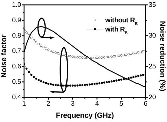
Fig. 2.12 anda significant noise power reduction in MOS device can be demonstrated by the additional resistor RB. A maximum 32% noise reduction can be achieved
without extra chip area, CMOS process steps and dc power. Fig. 2.13 shows the simulation results of noise figure with and without the additional resistor RB. It can be
observed that the 0.71/0.67/0.64 dB decrease in noise figure are attained at 2.5/3.5/5.2 GHz due to the usage of larger resistance RB=8 kΩ.
2.3.4 Simulation and Experimental Results
M
1V
DDM
2C
3V
g1R
gV
outV
inM
sw1V
g1L
dC
dV
contR
gV
g2R
gM
5R
1M
3M
4R
gC
2L
1C
1R
BR
BR
BR
BR
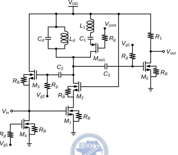
BFig. 2.14 Complete schematic of the proposed second triple-band LNA with the load network design and the noise reduction resistance RB.
are shown in Fig. 2.14 and Fig. 2.15, respectively. The die area including pads is 0.75×0.69 mm2, which has been measured by using on-wafer probing. The total dc power of the LNA chip without the output buffer is 14.2 mW. The simulated and measured results of S-parameters are depicted in Fig. 2.16. The measured peak gains are 12.3/15.3/13.1 dB at 2.5/3.5/5.2 GHz while the input and output return losses are better than 10 dB in the operation frequencies. The simulated and measured noise figures are depicted in Fig. 2.17 and the measured minimum noise figures at 2.5/3.5/5.2 GHz are 2.3/2.2/2.7 dB.
Fig. 2.15 Microphotograph of the second triple-band LNA with 0.75×0.69 mm2 die area.
2.0 2.5 3.0 3.5 4.0 4.5 5.0 5.5 6.0
-30
-20
-10
0
10
20
S11
S21
Measurement
Dual-Band Simulation
Single-Band Simulation
S-parameters (d
B)
Frequency (GHz)
(a)2.0 2.5 3.0 3.5 4.0 4.5 5.0 5.5 6.0
-80
-60
-40
-20
0
S22
S12
Measurement
Dual-Band Simulation
Single-Band Simulation
S-parameters (dB)
Frequency (GHz)
(b)Fig. 2.16 Measured and simulated S-parameters of the second triple-band LNA.
2.0
2.5
3.0
3.5
4.0
4.5
5.0
5.5
2.0
2.5
3.0
3.5
4.0
4.5
5.0
5.5
6.0
Measurement
Dual-Band Simulation
Single-Band Simulation
Noise Figure (dB)
Frequency (GHz)
2.4 SUMMARY
The triple-band LNAs with a switched resonator concept have been fabricated using 0.18-μm CMOS technology and a significant die area reduction can be achieved. Furthermore, an additional larger substrate resistor RB will diminish the output noise
power density of MOS device and the 0.71/0.67/0.64 dB noise figure decrease can be attained at 2.5/3.5/5.2 GHz in the second approach of the triple-band LNA without extra chip area, dc power and CMOS process steps. The measured results, including the power gain, the return loss, and the noise figure, agree quite well with the simulated results. The presented triple-band LNAs are compared with recently published CMOS LNA and summarized in Table 2.1.
Table 2.1
Performance summary of previously published LNAs Ref. Tech. [μm] Freq. [GHz] S11 [dB] Gmax [dB] NFmin [dB] Pdiss [mW] Area [mm2] [4] 0.18 3 ~ 6 <-12 15.9 4.7 59.4 1.1 [5] 0.18 2.8 ~ 7 <-4 19.1 3 32 1.63 [7] 0.18 dc ~ 7 <-16 8.6 4.2 9 1.16 [24] 0.13 2 ~ 5.2 <-9 16 4.7 38 0.24 [25] 0.09 2.5 ~ 4 <-10 10.6 4 16 0.77 [26] 0.13 3 ~ 5 <-10 19.4 Ψ 3.5 31.5 1.6 [27] 0.18 3 ~ 4.8 <-10 13.9 4.7 14.6 0.95 [28] 0.18 3 ~ 4.8 <-7 14.3 3.45 13.5 1.8 2.44 <-10 7.6 5.7 [29] 0.18 5.76 <-6 8.6 6.8 10.8 1.15 1.8 10.1 3.7 2.45 10.8 4.8 [9] 0.25 5.25 <-10 11.8 6.4 39.1 1.68 0.95 <-7 18 4.6 2.4 24 4.4 [30] 0.18 5.2 <-10 23 4.4 32.4 1.34 2.5 10 3.3 3.5 20.1 3.6 LNA1 0.18 5.2 <-10 11 4.6 10 0.92 2.5 12.3 2.3 3.5 15.3 2.2 LNA2 0.18 5.2 <-10 13.1 2.7 14.2 0.52
CHAPTER 3
DESIGN OF IMAGE-REJECTION MIXER FOR
DUAL-BAND OPERATION
3.1 INTRODUCTION
The down-conversion mixer, which converts the high RF frequency to a low IF frequency, is a required building block of the transceiver. It is also an important component associated with the linearity of the front-end receivers. In general, Gilbert cell is a typical type of the active mixers, and the Gilbert mixer consists of three stages: transconductor stage, switching stage, and load stage. The linearity of Gilbert mixer will be dominated by the transconductor stage if the switching stage is ideal. In order to get higher conversion gain, good isolation, and better dynamic and static offsets, and help to improve the second and third order intermodulation rejection, the double balanced Gilbert mixer with differential RF, LO, and IF signals are commonly used for optimum operation.
In addition, the suppression of the image signal is an essential requisite for the RF receiver design. Generally, the dual-band image rejection mixer can be achieved by either Hartley or Weaver architecture, but the image rejection characteristic is restricted due to the magnitude mismatch and phase error of the quadrature signal. On the other hand, the required dual-band mixer with quadrature signal generator for dual-band operation will further increase the complication of the circuit implementation,which is undesired for low-cost and low-power application. In this chapter, we adopt the differential, dual-band, third-order, active notch filter to
Fig. 3.1 Block diagram of the Hartley down-converter.
Fig. 3.2 Block diagram of the Weaver down-converter.
attenuate the dual-band image signal while maintaining a superior in-band performance and achieve smaller chip area and dc power consumption than previous circuits [32]-[35].
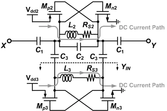
Fig. 3.3 Complete schematics of the proposed dual-band image rejection mixer.
3.2 CIRCUIT DESIGN
The proposed dual-band image rejection mixer fabricated by 0.18-μm TSMC CMOS process is shown in Fig. 3.3 with the target dual-band frequencies at 2.4~2.48 and 5.15~5.35 GHz. The common-source differential pair (M1 and M2) with one of the inputs grounded by a capacitor can be regarded as a single-ended to differential balun. In addition, the proposed mixer adopts a source-degenerated amplifier with a dual-band input network (Li, Ci, Lg) to achieve a 50 Ω match at 2.45 and 5.2 GHz. The
0.3 0.4 0.5 0.6 0.7 0.8 0.0 5.0m 10.0m
Bias Voltage V
G1(V)
|gm
| (A/V)
0.0 50.0m 100.0m|gm'|
(
A/V
2)
Fig. 3.4 The nonlinear effect of a transistor with the bias voltage VG1.
circuitry in between nodes X and Y is the proposed dual-band active notch filter to be discussed below.
3.2.1 Effect of Nonlinearity
In general, the nonlinear effect of a transistor in Fig. 3.4 is interrelated to the gate-to-source bias voltage and the second order transconductance coefficient gm′ could be minimized while the maximum linear transconductance gm is selected (i.e., the larger conversion gain, the superior second order harmonic suppression) [36]. Consequently, the second order harmonics behavior can be effectively diminished by adjusting the bias voltage VG1 to acquire a better conversion gain of mixer. Moreover,
the dominant gain contributor of the proposed mixer is the input transconductance stage M1–M2. To obtain a sufficient gain, we must raise the dc current of M1–M2 since
Fig. 3.5 A third-order notch filter reported in [37].
increase a small amount of dc power, the total dc power dissipation is still much smaller than previous circuits [32]-[35] made by the traditional Hartley or Weaver architectures.
3.2.2 Filter Design with Negative-Resistance Cells
Fig. 3.5 shows a third-order notch filter, which can provide low and high impedance at the image and wanted frequencies, respectively to effectively attenuate the image signal without deteriorating the in-band performance [37]. In this study, a differential dual-band image suppression circuitry based on the third-order notch filter topology is proposed and shown in Fig. 3.6 (a). In the following analyses, we utilize the half circuit in Fig. 3.6 (b) to facilitate the discussions. It is obvious that the parallel L-C section is inductive and capacitive at low and high frequencies, respectively; however, it is reversed for the series L-C section. If the resonance frequency is appropriately designed, the 0.5L2-2C2 and C3-0.5L3 circuit in Fig. 3.6 (b) at low frequency such as 2.45 GHz can be equal to an inductor Ltank and a capacitor Cseries
C
10.5L
20.5L
3Z
AC
3L
2L
3C
2C
1C
3C
3C
12C
2Z
A_diff+
-C
1L
tankZ
A@2.45 GHz
C
seriesC
1C
tankL
series(a)
(b)
(c)
(d)
Z
A@5.2 GHz
Fig. 3.6 (a) The proposed differential dual-band third-order notch filter. (b) The half circuit of (a). (c) Equivalent circuit at low frequency. (d) Equivalent circuit at high frequency.
shown in Fig. 3.6 (c).Similarly, Fig. 3.6 (d) can be acquired and comprehended by the above ratiocination. As a consequence, the proposed circuitry turns out to be the third-order notch filter in Fig. 3.5 at low and high frequencies simultaneously. After a straightforward derivation, the input impedance of the filter is given by
4 2
1 2 2 1
0.25 ( 2 ) (0.5 ) 1
s B C C s L C A
where A=L2C2+0.5L2C3+0.5L3C3, B=L2L3C3, from which two zeros and two poles can be obtained in the positive frequency domain to provide low impedance at dual image frequencies and high impedance at dual wanted frequencies, respectively.
The proposed differential dual-band third-order notch filter can be utilized for the 2.45/5.2 GHz WLAN application. However, it should be taken into account that the maximum attenuation of the image rejection filter is restricted by the series resistance of on-chip inductor. To overcome this limitation, the negative-resistance cell by using cross-coupled transistors can be employed to improve the Q value of on-chip inductor. In this study, the cross-connected pair consisted of NMOS and PMOS transistors as a negative conductance generator is used and shown in Fig. 3.7. Power consumption and the usage of inductors can be cut in half compared to the traditional approach while providing the same negative conductance. The dc current path will be provided by the on-chip inductor and the impedance YIN can be expressed as
3 3 3 3 3 2 3 3 3 3 3 3
1
(
)
(
)
gsn gsp S mn mp IN gsn gsp mn mpC
C
R
g
g
Y
j
j L
ω
C
C
ω
L
g
g
≈
+
+
−
+
+
(3.2)As can be seen in (3.2), sufficient negative resistance can be generated to eliminate RS3 by adjusting the bias voltage Vdd since the gmn,p is proportional to the current of
transistors. It is obvious that the negative resistance facilitates to improve the maximum attenuation of the image rejection filter, but an overlarge value will bring about stability problem. A trade-off between the image rejection performance and stability should be carefully considered so as to make an optimum design. To avoid stability problem in this design, the negative resistor must be smaller than the series resistance of on-chip inductor. On the other hand, the process variation and temperature will influence the bias currents of the transistors to further deteriorate the