Low temperature growth of carbon nanotubes on printing electrodes
by MPCVD
Kuang-Chung Chen
a,c,*, Chia-Fu Chen
a, Jih-Shun Chiang
b, Chian-Liang Hwang
b,
Yu-Yang Chang
c, Cheng-Chung Lee
caDepartment of Materials Science and Engineering, National Chiao Tung University, Taiwan, R.O.C. bUnion Chemica Laboratories (UCL), Industrial Technology Research Institute (ITRI), Hsinchu, Taiwan, 310, R.O.C. c
Electronics Research and Service Organization (ERSO), Industrial Technology Research Institute (ITRI), Hsinchu, Taiwan, R.O.C. Available online 15 August 2005
Abstract
In this work, combination of screen-printing process and microwave plasma enhanced chemical vapor deposition system (MPCVD) was applied to fabricate patterned carbon nanotubes (CNTs) on the cathode electrodes on glass substrates. Solution based Ni catalyst was well-mixed with Ag powders and organic binder materials to form screen printed paste. CNTs were then grown under the atmosphere of CH4/H2gas mixture
below 550-C. In the field emission measurement, the turn-on field was 3.2 V/Am and uniform electron emission image was also observed. D 2005 Elsevier B.V. All rights reserved.
Keywords: Carbon nanotubes; Glass substrates; MPCVD; Screen printing
1. Introduction
Carbon nanotubes (CNTs) were first discovered by Iijima in 1991 under transmission electron microscopy (TEM) observation [1]. Owing to the unique aspect ratios, CNTs exhibit excellent field emission characteristics such as low turn-on voltage and high current density. Numerous methods to grow CNTs have been developed, including arc-discharge, chemical vapor deposition and pulsed laser ablation[2 – 4]. Among various methods, both arc-discharge
[5]and CVD[6]were usually reported to be used for field emission display. A low cost process combining arc-discharge produced CNTs and screen-printing technologies was developed to prepare field emitters[7]. Unfortunately, using CNTs paste by screen-printing technology still needs a surface rubbing technology to improve field emission characteristics[7].
For CVD process, CNTs can directly grow on the predefined catalyst layer, and have high yield and uni-formity [8]. For FED applications, the growth temperature should be below 550 -C to avoid glass substrate deforma-tion. Recently, the studies of low temperature growth on glass substrates by CVD methods have been reported [9 – 11]. However, it is required to deposit pattern catalyst metals by semiconductor processes, which is much more expensive than screen-printing processes. Therefore, development of the CNT-FED at low temperature by a low cost technology will play an important role in practical FED applications. In this work, we successfully combined the advantages of screen-printing and MPCVD process to fabricate the pattern CNT-FED cathode at low temperature.
2. Experimental details
For preparing the catalysts, the silver (Ag) powders were dispersed in the water and then the ammonia (NH3) solution
was added at 100-C for 30 min. Next, Ni(NO3)2I6H2O was
added in the solution, and NH3solution also added in for
0040-6090/$ - see front matterD 2005 Elsevier B.V. All rights reserved. doi:10.1016/j.tsf.2005.07.085
* Corresponding author. Department of Materials Science and Enginee-ring, National Chiao Tung University, Taiwan, R.O.C. Fax: +886 3 5826842.
E-mail address: [email protected] (K.-C. Chen).
Thin Solid Films 498 (2006) 198 – 201
maintaining pH value at 10.5 at 100 -C for 3 h. The formaldehyde (HCHO) was added to make the nickel (Ni) ions deposit on Ag powders by heating at 100 -C for 30 min. Then the Ni/Ag powders were washed by DI water and dried at 110-C.
Dried Ni/Ag powders were then well-mixed with frit and organic vehicles by using ball mill and three-roller mill to make a printable paste. The Ni/Ag paste was coated on the soda-lime glass substrate by screen-printing technology. After printing, the Ag film was dried at 200-C for 1 h and heated at 400-C for 2 h to remove the organic materials in the paste, then the film was sintered at 560-C for 10 min. The sample was placed in a MPCVD (model IMG 2502-S, IDX Tokyo, Japan) chamber and evacuated at 10 2Torr. The Ag/Ni film was pretreated by hydrogen (H2) plasma for
5 min at microwave power 200 W. The flow rate and the total pressure for the pretreatment were 200 sccm and 6 Torr, respectively. Then the CNTs were grown using gas mixtures of 10 sccm methane and 10 sccm H2 under the
total pressure of 6 Torr. The microwave power was 150 W and growth time was kept at 30 min.
The morphology and structure of CNTs were observed by scanning electron microscope (SEM, Hitachi S-4000), trans-mission electron microscope (TEM), and Raman spectro-scope. The field emission behavior of CNTs was characte-rized in the diode method, with an ITO coated glass as anode and a spacer of 100 Am. The current – voltage characteristics were measured using Keithley 237 under 10 6Torr.
3. Results and discussion
The surface morphology of catalyst-Ni on Ag film after hydrogen plasma activating treatment is illustrated inFig. 1, showing that Ni nanoparticles were formed after treatment.
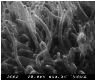
Figs. 2 and 3a show the SEM and TEM images of CNTs,
respectively. Ni catalytic nanoparticles were observed at the ends of the tubes, implying the tip growth mechanism
[12,13]. Carbon-containing gas was decomposed into
carbon atoms under plasma pyrolysis process and reacted with Ni catalytic metals. The carbon atoms diffused around the metal particles, and precipitated at the side of particles. As the process proceeded, the CNTs were formed and lifted up the metal from the substrate. It has been proposed that the surface melting point of nanoparticles can be as low as 40% of the bulk melting point by the surface curvature effect [14,15]. In addition, Ni nanoparticle could form a eutectic mixture with carbon and/or hydrogen, which can also reduce the melting point. According to both mecha-nisms described above, the melting point of Ni can be effectively reduced from 1450 -C and CNT synthesis temperature is as low as 550-C in our system.
The herringbone-like type structure multiwall carbon nanotubes (MWNT) were observed, and the diameter was in range of 40 – 50 nm. It was also observed that the CNTs were not straight and the crystalline graphite layers were not as good as those grown at high temperature[16,17]. At low temperature below 550-C, carbon atoms synthesized at the edge of the tubes do not have enough driving force and time to diffuse, and thus formed defective edges with pentagons and heptagons, which will eventually induce the curvature of nanotubes. Many researchers reported that more curved CNTs are produced under lower temperature[11,12]. Besides CNTs, a few of carbon nanofibers were also produced, as shown inFig. 3b. The formation of amorphous carbons was observed. The diameter of nanofibers was about 60 – 70 nm. In the previous studies, many researchers reported that the synthesis of carbon nanotubes accompanying production of carbon nanofibers at low temperature[10,18].
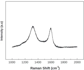
Carbon nanotubes were also characterized by Raman spectroscopy[19]. 1360 (D peak) and 1590 cm 1(G peak) were observed in Raman spectrum, as shown inFig. 4. Peak at 1360 cm 1 is related to disordered graphite structure. This spectrum peak indicates that amorphous carbons exist at the wall of CNTs. The other spectrum peak at 1590 cm 1 corresponding to the high frequency E2gfirst-order mode of
Fig. 1. SEM image of surface morphology of catalyst-Ni on Ag film after hydrogen plasma activating treatment.
Fig. 2. SEM image of surface morphology of CNTs grown at 6 Torr with 10 sccm CH4and 10 sccm H2.
graphite structure[20]indicates the formation of graphitized carbon nanotubes. The intensity of D peak relative to the G peak, ID/IG, is about 2.33. This means that amorphous
carbons adhered at CNT walls, a small amount of carbon nanofibers produced, and defective pentagon and heptagon structure in the graphitized walls exist due to low growth temperature[19,21]. It can be observed clearly in the TEM images as shown inFig. 3a and b.
Fig. 5 shows the emission current density vs. electric field curve and the corresponding Fowler – Nordheim (F – N) plots. A turn-on field was defined as the field to give an emission current density of 10 AA/cm2. The turn-on field value at this case was 3.2 V/Am. The turn-on field value of non-aligned MWNTs is well agreed by earlier reports
[19,22]. If ln(I/E2) vs. 1/E in the F – N plot was a straight line, this indicated that field electron emission was intrinsi-cally driven by electric field. However, in agreement with many other works [23,24], the ln(I/E2) vs. 1/E exhibits a line in the intermediate range but shows saturation at higher fields. Actually, the current density of 0.1 mA/cm2is known to be sufficient for practical displays operating.Fig. 6shows the emitting image of the anode (coated by the green phosphor) at the electric field of 10 V/Am.
1000 1200 1400 1600 1800 2000
Intensity (a.u)
Raman Shift (cm-1)
Fig. 4. Raman spectrum at the surface of the sample.
0 2 4 6 8 10 12 0.0000 0.0004 0.0008 0.0012 0.0016 0.0010 0.0012 0.0014 -24 -23 -22 ln(I/V 2) 1/V
Current Density (A/cm
2 )
Applied Field (V/µm)
Fig. 5. Emission current density vs. electric field curve. Inserted curve is Fowler – Nordheim plot.
Fig. 6. Emission image at applied field 10 V/Am. Fig. 3. TEM images of the sample: (a) herringbone-like carbon nanotube (b)
carbon nanofiber. The sample was grown at 6 Torr with 10 sccm CH4and
10 sccm H2.
K.-C. Chen et al. / Thin Solid Films 498 (2006) 198 – 201 200
4. Conclusion
We successfully combined the advantages of screen-printing process and MPCVD process to pattern catalyst/Ag cathode and grow CNTs on patterned Ni-catalyst of cathode electrode on glass substrates below 550 -C. Carbon nano-tubes can be grown at total pressure 6 Torr with a CH4flow
rate of 10 sccm and H2flow rate of 10 sccm for 30 min.
Both herringbone-like type structure multiwall carbon nanotubes (MWNT) and nanofibers were observed. The turn-on field value at this case was 3.2 V/Am. Uniform electron emission was also observed on the electrode with good emission current and brightness.
References
[1] S. Iijima, Nature 354 (1991) 56.
[2] P.G. Collins, A. Zettl, Appl. Phys. Lett. 69 (1996) 1969.
[3] S. Fan, M.G. Chapline, N.F. Franklin, T.W. Tombler, A.M. Cassel, H. Dai, Science 283 (1999) 512.
[4] Q.H. Wang, A.A. Setlur, J.M. Lauerhass, J.Y. Dai, E.W. Seeling, R.P.H. Chang, Appl. Phys. Lett. 72 (1998) 2912.
[5] P.G. Collins, A. Zettl, Phys. Rev., B 55 (1997) 9391.
[6] Y. Chen, D.T. Shaw, L. Guo, Appl. Phys. Lett. 76 (2000) 2469. [7] W.B. Choi, D.S. Chung, J.H. Kang, H.Y. Kim, Y.W. Jin, I.T. Han, Y.H. Lee, J.E. Jung, N.S. Lee, G.S. Park, J.M. Kim, Appl. Phys. Lett. 75 (1999) 3129.
[8] G.S. Choi, Y.S. Cho, S.Y. Hong, J.B. Park, K.H. Son, D.J. Kim, J. Appl. Phys. 91 (2002) 3847.
[9] H.S. Kang, H.J. Yoon, C.O. Kim, J.P. Hong, I.T. Han, S.N. Cha, B.K. Song, J.E. Jung, N.S. Lee, J.M. Kim, Chem. Phys. Lett. 349 (2001) 196.
[10] C.J. Lee, J. Park, S. Han, J. Ihm, Chem. Phys. Lett. 337 (2001) 398. [11] J.-H. Han, S.H. Choi, T.Y. Lee, J.-B. Yoo, C.-Y. Park, H.J. Kim, I.-T. Han, S. Yu, W. Yi, G.S. Park, M. Yang, N.S. Lee, J.M. Kim, Thin Solid Films 409 (2002) 126.
[12] Y.C. Choi, D.J. Bae, Y.H. Lee, B.S. Lee, I.T. Han, W.B. Choi, N.S. Lee, J.M. Kim, Synth. Met. 108 (2000) 159.
[13] W.Z. Li, S.S. Xie, L.X. Qian, B.H. Chang, B.S. Zou, W.Y. Zhou, R.A. Zhao, G. Wang, Science 274 (1996) 1701.
[14] M.H. Kuang, Z.L. Wang, X.D. Bai, J.D. Guo, E.G. Wang, Appl. Phys. Lett. 76 (2000) 1255.
[15] Z.L. Wang, J.M. Petroski, T.C. Green, M.A. El-Sayed, J. Phys. Chem., B 102 (1998) 6145.
[16] C.J. Lee, J. Park, S.Y. Kang, J.H. Lee, Chem. Phys. Lett. 323 (2000) 554.
[17] C.J. Lee, J. Park, S.Y. Kang, J.H. Lee, Chem. Phys. Lett. 326 (2000) 175.
[18] H. Neumayer, R. Haubner, Diamond Relat. Mater. 13 (2004) 1191. [19] M. Sveningsson, R.-E. Morjan, O.A. Nerushev, Y. Sato, J. Ba¨ckstro¨m,
E.E.B. Campbell, F. Rohmund, Appl. Phys., A 73 (2001) 409. [20] T.C. Chieu, M.S. Dresselhaus, M. Endo, Phys. Rev., B 26 (1982)
10530.
[21] P.C. Eklund, J.M. Holden, R.A. Jishi, Carbon 33 (1995) 959. [22] J.-M. Bonard, H. Kind, T. Stockli, L.-O. Nilsson, Solid State Electron.
45 (2001) 893.
[23] X. Xu, G.R. Brandes, Appl. Phys. Lett. 74 (1999) 2549.
[24] H. Murakami, M. Hirakawa, C. Tanaka, H. Yamakawa, Appl. Phys. Lett. 76 (2000) 1776.