國立交通大學
電子工程學系 電子研究所碩士班
碩士論文
利用高介電長數 HfAlO 之元素含量做為阻擋層
應用在非揮發性記憶體上之研究
Study on High-k Gate dielectric
Hf
1-x
Al
x
O for Blocking layer of SONOS
Non-Volatile Memory
研究生:顧春瑀
指導教授:雷添福 博士
利用高介電長數 HfAlO 之元素含量做為阻擋層應用在非揮
發性記憶體上之研究
Study on High-k Gate dieletric Hf
1-xAl
xO for Blocking layer
of SONOS Non-Volatile Memory
研 究 生:顧春瑀 Student:Chun-Yu Ku
指導教授:雷添福 Advisor:Dr. Tan Fu Lei
國 立 交 通 大 學
電子工程學系 電子研究所碩士班
碩 士 論 文
A Thesis
Submitted to Department of Electronics Engineering & Institute of Electronics College of Electrical Engineering & Computer Science
National Chiao Tung University In Partial Fulfillment of the Requirements
For the Degree of Master of Science
in
Electronic Engineering August 2008
Hsinchu, Taiwan, Republic of China
利用高介電長數 HfAlO 之元素含量做為阻擋層
應用在非揮發性記憶體上之研究
學生 : 顧 春 瑀 指導教授: 雷 添 福 博士
國立交通大學
電子工程學系 電子研究所碩士班
摘要
在本論文的第二章中,我們討論不同成分的 Hf1-xAlxO 在經過不同溫度的退火 處理所產生的變化。我們利用有系統的方法來萃取我們所需要的最好的條件。我 們期望在記憶體在寫入與抹除操作時扮演重要的角色,而沒有過大的漏電流存 在。 在本論文的第三章中,我們提出一個利用高介電係數 HfAlO 還有氧化鋁作為 阻擋層的 SONOS 非揮發性記憶體。雖然氧化鋁一直是一個做為阻擋層的很好的材 料,但是由於他的 k 值不夠高,所以寫入以及抹除的速度不是非常明顯的快速。 所以我們增加一些 Hf 的材質進入氧化鋁裡面,以期望能提高 k 值。從上面的第 二章的一些資料中,我們萃取出最好的條件做為我們的阻擋層。並且測量記憶體 的電性,將 HfAlO 以及氧化鋁互相比較。 III
Study on High-k Gate dieletric Hf
1-xAl
xO for
Blocking layer of SONOS Non-Volatile Memory
Student: Bobby Ku Advisor: Dr. Tan-Fu Lei
Department of Electronics Engineering &
Institute of Electronics
National Chiao Tung University
ABSTRACT
In chapter 2, we discuss the dependence of different Hf1-xAlxO componont
dielectric on the different annealing temperatures. We used a systematic methodology to extract the best result for our blocking layer of SONOS-type memories. We expect the high-k blocking layer can play a key role in program/erase speed without large leakage current.
In chapter 3, we purpose the SONOS-type nonvolatile memory with high-k HfAlO and Al2O3 blocking layer. Although Al2O3 is a good material for
blocking layer of SONOS memory, the program/erase speed is not obvious faster attributed to the k is not high enough. So we add the Hf into Al2O3
for our blocking layer in order to increase the k. From the data in chapter 2, we use the best condition for our blocking layer. We also measure the memory characteristic to compare Al2O3 and HfAlO.
致謝
首先要向我的指導教授雷添福老師致上最大的謝意,因為在老師的關心指導 還有尊尊教誨下,我的論文才得以完成。由於老師採取信任的態度,讓學生自由 的發揮創意做實驗,在報告進度時提供了寶貴的意見,讓我這兩天過得非常充 實,學到許多實用的東西。 再來,我想謝謝鄭兆欽學長跟楊紹明學長,在我一開始進入研究所的時候他 們非常照顧我,也帶我做實驗。另外,我最感謝的是張家文學長,在我實驗進度 落後的時候拉我一把,並且還指導我很多東西,讓我能夠順利的畢業;還有黃博, 在我遇到問題的時候他都盡量幫我解決。也要謝謝一起做實驗的李旭恆、正妹 凱、show、土豆、簡嘉宏還有張嘉文!!沒有他們的大力幫助我的進度可能落後 又落後了;還要大力的感謝正愷兄,在我最後口試以及量測上提供寶貴的建議。 也要謝謝實驗室其他的學長:搞笑的小 P 學長、很忙的羅大學長,還有冠良,都 在最後的時候提供我一些口試的意見;也祝福你們實驗順利。還有一些已經畢業 的學長:志仰、伯儀、余博、哲倫,很感謝你們辛苦的照顧我。 另外,也要謝謝 samo 哥、砲政哥哥、洋 A、猛男、綺哥、小黛哥、沈佑書、 黃義涵、暴走以及翁啟祥在修課的時候給了我很大的幫助,還要感謝宣凱、效喻、 弘森、欣哲以及孝瑜幫我做 ALD,還有可愛的乾妹雨蓁以及曉萱都幫我很多。 最後,我要感謝我母親,這幾年辛苦她了,還有我姊姊,這段時間沒有他們 的全力支持,我是不會走到這一步的;最後最後,也謝謝這段時間陪我的筱君, 在我最艱苦的時候陪伴我走過!!!謝謝你們。 IIIContents
Abstract (Chinese)... I
Abstract (English)... II
Acknowledge... III
Contents………..IV
Table & Figure Captions………...VI
Chapter 1 Introduction………...1
1-1 Overview of Flash Memory...1
1-2 Motivation...4
1-3 Thesis Organization...6
Chapter 2 Physical and Electrical properties of MIS Capacitors Using MOCVD Hf1-xAlxO Dieletrics...11
2-1 Introduction ...11
2-2 Experimental...13
2-3 Results and Discussion...14
2-3-1 C-V Characteristics...14
2-3-2 I-V Characteristics...14
2-3-3 CET Characteristics...15
V
2-4 Summary...16
Chapter 3 Characteristics of SONOS-type Memory with High-k Hf1-xAlxO Blocking Layer …………...……...32
3-1 Introduction...32
3-2 Experimental...33
3-3 Results and Discussion...34
3-3-1 Ig-Vg curves and Memory Window...34
3-3-2 Program and Erase Speed...35
3-3-3 Data Retention Characteristic……….36
3-3-4 Disturbance Measurement………..36 3-4 Summary...37 Chapter 4 Conclusions...56 Reference……….58 Chapter 1………..58 Chapter 2………..63 Chapter 3………..…65
Figure Captions
Chapter 1
Fig. 1-1: The semiconductor memory tree……….7
Fig. 1-2: The semiconductor memory………7
Fig. 1-3: The floating gate (FG) structure. The polysilicon is used as floating gate to
storage data………...8
Fig. 1-4: Current-voltage characteristic of a memory device in the erased and
programmed state, showing the Vth shift and the memory window………...8
Fig. 1-5: The conventional SONOS memory structure. Silicon nitride is used as
charge trapping layer………..9
Fig. 1-6: The band diagram of nitride- based SONOS memory………9
Fig. 1-7: The calculated gate leakage for low standby power (LSTP) application
[1.21]………10
Chapter 2
Fig. 2-1: Bandgap and band alignment of high k gate dielectrics with respect to
silicon………...17
Fig. 2-2: The process flow of the Hf1-xAlxO MOS capacitors………..17
Fig. 2-3: The relationship between Hf/Al precursor rate and Hf/Al ratio in
Hf1-xAlxO………..18
Fig. 2-4: The C-V curves of Al2O3 dielectric MOS capacitor………..19
Fig. 2-5: The C-V curves of H1A2 (Hf/Al = 0.11) dielectric MOS capacitor……….19
Fig. 2-6: The C-V curves of H1A1 (Hf/Al = 0.23) dielectric MOS capacitor……….20
Fig. 2-7: The C-V curves of H2A1 (Hf/Al = 0.55) dielectric MOS capacitor……….20
Fig. 2-8: The C-V curves of H6A1 (Hf/Al = 3) dielectric MOS capacitor…………..21
Fig. 2-9: The C-V curves of H8A1 (Hf/Al = 4) dielectric MOS capacitor…………..21
Fig. 2-10: The C-V curves of H10A1 (Hf/Al = 5.67) dielectric MOS capacitor…….22
Fig. 2-11: The C-V curves of HfO2 dielectric MOS capacitor……….22
Fig. 2-12: The I-V curves of Al2O3 dielectric MOS capacitor……….23
Fig. 2-13: The I-V curves of H1A2 (Hf/Al = 0.11) dielectric MOS capacitor……….23
Fig. 2-14: The I-V curves of H1A1 (Hf/Al = 0.23) dielectric MOS capacitor……….24
Fig. 2-15: The I-V curves of H2A1 (Hf/Al = 0.55) dielectric MOS capacitor……….24
Fig. 2-16: The I-V curves of H6A1 (Hf/Al = 3) dielectric MOS capacitor…………..25
Fig. 2-17: The I-V curves of H8A1 (Hf/Al = 4) dielectric MOS capacitor…………..25
Fig. 2-18: The I-V curves of H10A1 (Hf/Al = 5.67) dielectric MOS capacitor……...26
Fig. 2-19: The I-V curves of HfO2 dielectric MOS capacitor………..…26
Fig. 2-20: The gate leakage current comparison between H1A2 and Al2O3 with the
same condition (As-dep., 600oC PDA and 800oC PDA)………27
Fig. 2-21: The relationship between interfacial state density Dit and PDA
conditions………...…27
Fig. 2-22: The relationship between the gate leakage current Jg@Vfb-2V(A/cm2) and
each sample for all conditions………28
Fig. 2-23: The relationship between the gate leakage current Jg@Vfb-2V(A/cm2) and
the CET for each samples with all PDA conditions………...28
Fig. 2-24: The relationship between CET (nm) and each Al-rich-Hf1-xAlxO samples
with all PDA conditions……….…29
Fig. 2-25: The relationship between the gate leakage current Jg@Vfb-2V(A/cm2) and
each Al-rich-Hf1-xAlxO samples with all PDA conditions………..29
Fig. 2-26: The relationship between the gate leakage current [email protected](A/cm2) and
each Al-rich-Hf1-xAlxO samples with all PDA conditions………..30
Fig. 2-27: The relationship between the gate leakage current Jg@Vfb-2V(A/cm2) and
the CET for each samples with all PDA conditions………...30
Chapter 3
Fig. 3-1: The process flow and the cross-section of the n+ poly gate flash memory………38~41
Fig. 3-2: The relationship between gate leakage current Jg (A/cm2) and gate electric
field Vg/EOT (MV/cm)……….41
Fig. 3-3: The Id-Vg curves of the Al2O3 blocking layer flash memory in the fresh,
programmed, and erased state at different conditions………..42
Fig. 3-4: The Id-Vg curves of the HfAlO blocking layer flash memory in the fresh,
programmed, and erased state at different conditions………..42
Fig. 3-5: The program speed curves of SONOS-type memory with Al2O3 (700oC PDA)
blocking layer. (CHEI mechanism)………..43
Fig. 3-6: The program speed curves of SONOS-type memory with Al2O3 (As-dep.)
blocking layer. (CHEI mechanism)………..43
Fig. 3-7: The program speed curves of SONOS-type memory with HfAlO (700oC PDA) blocking layer. (CHEI mechanism)………44
Fig. 3-8: The program speed curves of SONOS-type memory with HfAlO (As-dep.)
blocking layer. (CHEI mechanism)………..44 Fig. 3-9: The comparison program speed curves of SONOS-type memory with Al2O3
and HfAlO (700oC PDA) blocking layer. (CHEI mechanism)………45 Fig. 3-10: The comparison program speed curves of SONOS-type memory with Al2O3
and HfAlO (As-dep.) blocking layer. (CHEI mechanism)……….45 Fig. 3-11: The program speed curves of SONOS-type memory with Al2O3 (700oC
PDA) blocking layer. (FN tunneling mechanism)………46
Fig. 3-12: The program speed curves of SONOS-type memory with Al2O3 (As-dep.)
blocking layer. (FN tunneling mechanism)………46
Fig. 3-13: The program speed curves of SONOS-type memory with HfAlO (700oC PDA) blocking layer. (FN tunneling mechanism)………..47
Fig. 3-14: The program speed curves of SONOS-type memory with HfAlO (As-dep.)
blocking layer. (FN tunneling mechanism)………....47
Fig. 3-15: The comparison program speed curves of SONOS-type memory with all
devices. (FN tunneling mechanism with Vg = 15V)………..48
Fig. 3-16: The erase speed curves of SONOS-type memory with Al2O3 (700oC PDA)
blocking layer. (Band To Band Hot Hole mechanism)………...…48
Fig. 3-17: The erase speed curves of SONOS-type memory with Al2O3 (As-dep.)
blocking layer. (Band To Band Hot Hole mechanism)………...49
Fig. 3-18: The erase speed curves of SONOS-type memory with HfAlO (700oC PDA) blocking layer. (Band To Band Hot Hole mechanism)………...49
Fig. 3-19: The erase speed curves of SONOS-type memory with HfAlO (As-dep.)
blocking layer. (Band To Band Hot Hole mechanism)………...50
Fig. 3-20: The comparison program speed curves of SONOS-type memory with all
devices. (Band To Band Hot Hole mechanism with Vg=-5V
Vd=9V)………...…50
Fig. 3-21: The retention characteristic of SONOS-type flash memory with Al2O3
(As-dep. and 700oC PDA) blocking layer at 25oC……….…51
Fig. 3-22: The retention characteristics of SONOS-type flash memory with HfAlO
(As-dep. and 700oC PDA) blocking layer at 25oC……….…51 Fig. 3-23: The charge loss rate characteristics of SONOS-type flash memory with all
devices at 25oC………...…52
Fig. 3-24: The gate disturbance characteristics of SONOS-type flash memory with
Al2O3 (As-dep. and 700oC PDA) blocking layer. (Erase State)………...52
Fig. 3-25: The gate disturbance characteristics of SONOS-type flash memory with
HfAlO (As-dep. and 700oC PDA) blocking layer. (Erase State)…………53 Fig. 3-26: The gate disturbance characteristics of SONOS-type flash memory with all
samples. (Erase State)……….53
Fig. 3-27: The gate disturbance characteristics of SONOS-type flash memory with
Al2O3 (As-dep. and 700oC PDA) blocking layer. (Program State)………54
Fig. 3-28: The gate disturbance characteristics of SONOS-type flash memory with
HfAlO (As-dep. and 700oC PDA) blocking layer. (Program State)…...…54 Fig. 3-29: The gate disturbance characteristics of SONOS-type flash memory with all
samples. (Program State)………....55
Fig. 3-30: The read disturbance characteristics of SONOS-type flash memory with all
samples. (Program State)………..……..55
XII
Table Captions
Chapter 1
Table 1-1: Scaling parameters for 2001 ITRS………..10
Chapter 2
Table 2-1: Selected material and electrical properties of high-k gate dielectrics…….16
Table 2-2: Split table for MIS Capacitors using MOCVD Hf1-xAlxO Dielectric…….18
1
Chapter 1
Introduction
1-1 Overview of Flash Memory
Semiconductor memory is an indispensable component of modern electronicsystem. It is used in personal computers, cellular phones, digital cameras , smart-media, networks, automotive systems, global positioning systems.
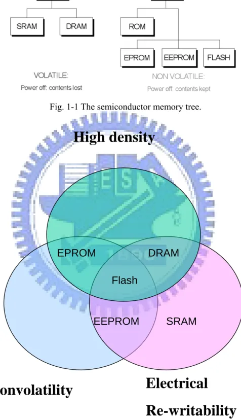
The memories based on complementary metal-oxide-semiconductor (CMOS) technology can be divided into two main categories by whether the storage data can be affected by the power supply as depicted in Fig. 1-1:
─The volatile memory: like SRAM and DRAM .
SRAM memory can retain the stored information as long as the power is on, drawing very little current. However, the information will be lost when the power is turned off, so SRAM is not a nonvolatile memory.
A Dynamic Random Access Memory (DRAM) cell consists of one transistor and one capacitor. Compared to flash memory, DRAM has much faster program/read speed with very low operating voltage, while flash memory needs 1us to 1ms programming time and high programming voltage. Unfortunately, DRAM is a volatile memory.
─The non-volatile memory: this kind memory will keep the storage data even if the power supply is off, like electrically programmable read only memory (EPROM), electrically erasable programmable read only memory (EEPROM), and the flash memory. Fig. 1-2 shows the semiconductor memory .
2
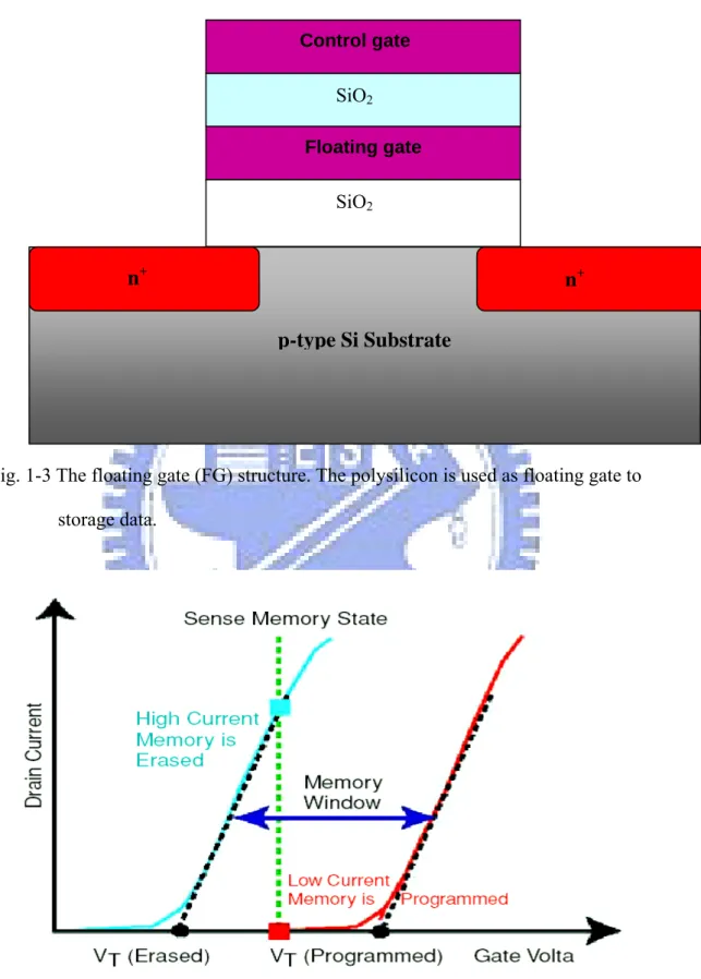
memory. The advantages of Flash memory are that it can be electrically written more than 100K times with byte programming and sector erasing and with the smallest cell size (one transistor cell) [1.1]-[1.2]. The Flash memory cell is used floating gate (FG) structure as illustrated in Fig. 1-3.
S. M. Sze and D. Kahng, invented the first floating-gate (FG) nonvolatile semiconductor memory in 1967 [1.3]. The conventional FG memory (in Fig. 1-3) used polysilicon as a charge storage layer surrounded by the dielectric [1.1]. Fig. 1-4 shows a typical current versus gate voltage characteristic of an erased FG memory and its Vt shift when the FG memory is programmed. The memory-state for the device can be determined by measuring the current in the MOSFET when a control gate bias is applied within the memory window.
The FG structure can achieve high densities, good program/erase speed and good reliability for Flash memory application. However, the FG memory has several drawbacks. Firstly, the Flash memory needs thick tunnel oxide (8~10nm) to provide superior retention and endurance characteristics, but it also causes higher operation voltage, slow P/E speed, and poor scalability issues. Secondly, because the polysilicon floating-gate is conductive, the total charges stored in floating-gate will be easily leaked directly through the tunnel oxide when the tunnel oxide is damaged during P/E cycles [1.4]. In order to improve the write/erase speed of a floating-gate device, the thickness of the tunnel oxide must be reduced. The tunnel oxide must be less than 25Å in order to achieve 100 ns write/erase time for a reasonable programming voltage (<10 V). Unfortunately, the retention time will be too short. Stress- induced leakage current (SILC) will further degrade the retention time.
The floating gate memory requires thick tunnel oxide to prevent charge loss through the defect. In order to solve the scaling issue of FG memory, the poly Si- Oxide-Nitride-Oxdie-Silicon (SONOS) memory has been studied recently [1.4].
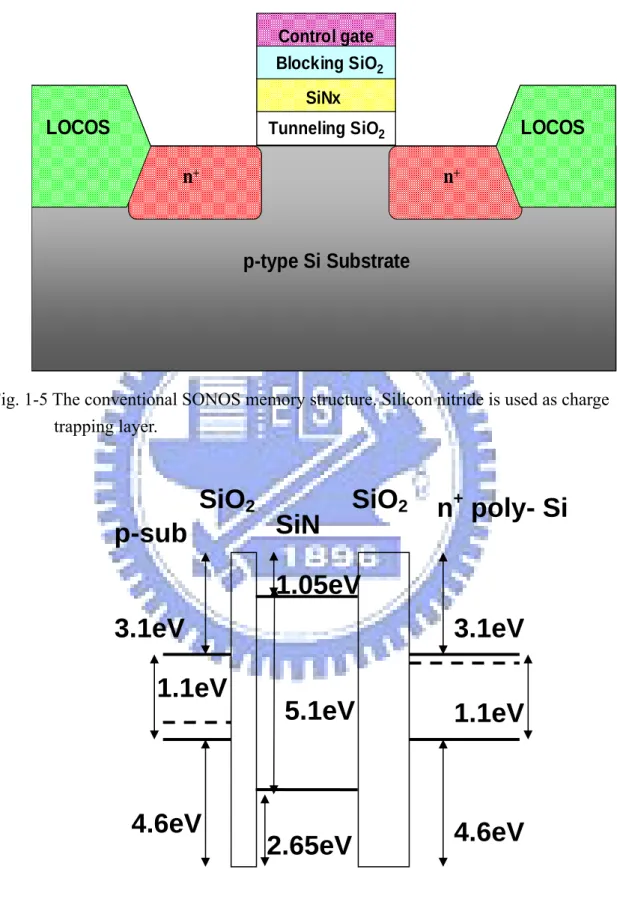
3
SONOS memory has better charge retention than floating gate memory when floating gate tunneling oxide is below 10nm due to its isolated deep-level traps. Hence, a leakage path in the tunneling oxide will not cause the discharge of the memory cell [1.4]. The structure of SONOS memory is shown in Fig. 1-5. The SONOS memory uses silicon nitride as charge trapping layer, and the band diagram is shown in Fig. 1-6. The conduction band offset between silicon substrate and nitride is 2.05eV. When we apply a positive voltage on the gate, the band will bend downward as illustrated in Fig. 1-6 [1.5]. The electrons in the Si-sub conduction band will tunnel through the tunneling oxide and a portion of nitride to be trapped in the charge trapping layer.
In order to improve program/erase (P/E) speed, the tunnel oxide thickness should be scaled to maximize the Fowler–Nordheim tunneling probability. However, to avoid the degradation of retention characteristics by tunneling leakage through ultrathin tunnel oxide, the optimization of the tunnel oxide thickness is necessary [1.7]. The optimization of the blocking layer is also necessary to avoid electron tunneling through the blocking oxide during the erase condition, which in turn causes an undererased problem [1.6, 1.8]. Since the high-k dielectric exhibits a significantly lower leakage current density for the relatively thinner effective oxide thickness, we can increase both the thickness and the electric field for the tunnel oxide at the same operating voltage. Therefore, a SONOS-type flash device with high-k dielectrics for a blocking layer provides a faster P/E speed and longer data retention time [1.9].
Besides, continued device scaling requires the continued reduction of the gate dielectric thickness. This requirement arises from two different considerations: controlling the short-channel effect and achieving a high current drive by keeping the amount of charge induced in the channel large as the power-supply voltage decreases. In both cases, to a first approximation, it is the electrical thickness that is important. The electrical thickness at inversion is determined by the series combination of three
4
capacitances in the gate stack: the depletion capacitance of the gate electrode, the capacitance of the gate dielectric, and the capacitance of the inversion layer in the silicon. On the other hand, the direct tunneling current through the gate dielectric grows exponentially with decreasing physical thickness of the gate dielectric [1.10]. This tunneling current has a direct impact on the standby power of the chip and puts a lower limit on unabated reduction of the physical thickness of the gate dielectric. It is likely that tunneling currents arising from silicon dioxides (SiO2) thinner than 0.8 nm
cannot be tolerated, even for high-performance systems [1.11]. Solutions that reduce the gate tunneling current and gate capacitance degradation due to polysilicon depletion are explored through introduction of new materials: high-dielectric-constant gate dielectrics.
1-2 Motivation
Today the key dielectrics such as SiO2 and Si3N4 are widely used in the modern
silicon devices. Aggressive scaling of CMOS devices and design of DRAM stimulates the investigation of alternative to SiO2 and Si3N4 high dielectric constant (high-k)
dielectrics, such as Al2O3, HfO2, ZrO2, Ta2O5, etc. [1.12, 1.13]. Since 1990
nonvolatile semiconductor memory (NVSM) has been the technology driver of the semiconductor industry [1.14]. At the present time a floating gate FLASH EEPROM dominates in the NVSM market. The floating gate type of FLASH EEPROM is impossible to scale down to beyond 0.18 μm due to the difficulty in scaling the tunnel oxide [1.15]. However, for design of terabit EEPROM memory array it is necessary to use the channel length of 30–40 nm. On contrary, a silicon–oxide–nitride–oxide–silicon (SONOS) EEPROM potentially can be scaled up to this size [1.16, 1.17]. Recently SONOS with thick bottom oxide was proposed,
where write/erase (W/E) is produced due to hot electron/hole injection in nitride [1.18, 1.19]. Also there were attempts to use SONOS as DRAM devices [1.20].
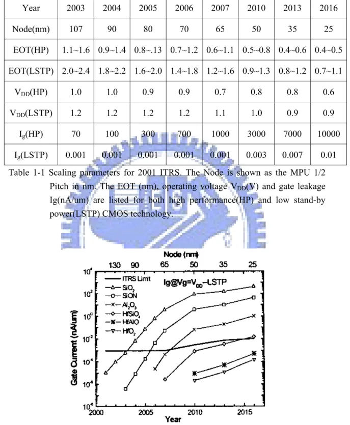
From [1.21], Fig. 1-7 shows that SiO2 will approach the scaling limits (Table 1-1,
2001 ITRS) in 2003 due to its high gate leakage, High-k (HfO2, HfAlO and Al2O3)
can extend the CMOS technology scaling for long-term solutions. Beside, SiO2 is
usually applied as a top oxide in a conventional SONOS. Since SiO2 has low
dielectric constant =3.9 in comparison with Si3N4 ( =7.5) the electric field in top
oxide is about two time larger, than in nitride. Therefore, for scaled SONOS device with comparable thickness of nitride and SiO2 top oxide, a remarkable part of applied
voltage drops on the top oxide during W/E programming. Replacing SiO2 by high-k
dielectric can decrease this undesirable voltage drop and, consequently, the total applied voltage [1.22, 1.23, 1.24]. Moreover, because of an electric field in high-k dielectric much less than one in SiO2, one can expect that parasitic carrier injection
[1.25] through top oxide should be suppressed in SONOS with high-k dielectric as a top layer. These suppositions were supported by experiment with SONOS with Al2O3
as a blocking oxide [1.23] and by preliminary simulations of W/E process in SONOS with Al2O3 and ZrO2 as a top oxide [1.24].
The goal of this paper is more detail investigation on the characteristics of SONOS type memory with high-k dielectrics instead of conventional SONOS with SiO2 as a top blocking dielectric. This also includes the description of the physical
and electrical properties of metal-insulator-metal capacitors, which play a great role of our n-channel SONOS type memory. As example we considered Al2O3 ( =9), HfAlO
( =9~25) and HfO2 ( =25) as mostly studied high-k dielectrics.
6
1-3 Thesis Organization
In this thesis, we study the performance of the SONOS-type memory device with high-k dielectric as blocking layer using MOCVD.
In Chapter 1, we introduce the background of the flash memory and explain why SONOS-type memory with high-k blocking layer.
In Chapter 2, we fabricate metal-insulator-metal capacitors using MOCVD HfAlO dielectric, measuring C-V and I-V. And then we discuss the physical and electrical properties in order to extract the excellent result to fabricate n-channel SONOS type memories device.
In Chapter 3, we fabricate n-channel SONOS type memories using HfAlO for blocking layer. And then we discuss the advantages and weak points of them.
Fig. 1-1 The semiconductor memory tree.
7
Fig. 1-2 The semiconductor memory.
Nonvolatility
Electrical
Re-writability
High density
EPROM DRAM
Flash
EEPROM
SRAM
8
Fig. 1-3 The floating gate (FG) structure. The polysilicon is used as floating gate to storage data.
Fig. 1-4 Current-voltage characteristic of a memory device in the erased and programmed state, showing the Vth shift and the memory window.
Control gate SiO2 Floating gate SiO2 n+ n+ p-type Si Substrate
p-type Si Substrate
n
+LOCOS
n
+LOCOS
Control gate Blocking SiO2 Tunneling SiO2 SiNxp-type Si Substrate
n
+LOCOS
n
+LOCOS
p-type Si Substrate
n
+LOCOS
n
+n
+LOCOS
Control gate Blocking SiO2 Tunneling SiO2 SiNx Control gate Blocking SiO2 Tunneling SiO2 SiNxFig. 1-5 The conventional SONOS memory structure. Silicon nitride is used as charge trapping layer.
3.1eV
1.1eV
4.6eV
3.1eV
1.1eV
4.6eV
1.05eV
5.1eV
2.65eV
p-sub
SiO
2SiO
2SiN
n
+poly- Si
Fig. 1-6 The band diagram of nitride- based SONOS memory.
Year 2003 2004 2005 2006 2007 2010 2013 2016 Node(nm) 107 90 80 70 65 50 35 25 EOT(HP) 1.1~1.6 0.9~1.4 0.8~.13 0.7~1.2 0.6~1.1 0.5~0.8 0.4~0.6 0.4~0.5 EOT(LSTP) 2.0~2.4 1.8~2.2 1.6~2.0 1.4~1.8 1.2~1.6 0.9~1.3 0.8~1.2 0.7~1.1 VDD(HP) 1.0 1.0 0.9 0.9 0.7 0.8 0.8 0.6 VDD(LSTP) 1.2 1.2 1.2 1.2 1.1 1.0 0.9 0.9 Ig(HP) 70 100 300 700 1000 3000 7000 10000 Ig(LSTP) 0.001 0.001 0.001 0.001 0.001 0.003 0.007 0.01
Table 1-1 Scaling parameters for 2001 ITRS. The Node is shown as the MPU 1/2 Pitch in nm. The EOT (nm), operating voltage VDD(V) and gate leakage
Ig(nA/um) are listed for both high performance(HP) and low stand-by power(LSTP) CMOS technology.
Fig. 1-7 The calculated gate leakage for low standby power (LSTP) application. Here, an average value of the proposed maximum and minimum EOT from Table 1-1 is used for each generation. Al2O3 mole fraction is 30% for
HfAlO and Si3N4 mole fraction 40% for optimized SiON [1.21].
Chapter 2
Physical and Electrical properties of MIS
Capacitors Using MOCVD Hf
1-x
Al
x
O
Dieletrics
2-1 Introduction
A gate dielectric with a dielectric constant (k) substantially higher than that of SiO2 (kox) will achieve a smaller equivalent electrical thickness (teq) than the SiO2, even
with a physical thickness (tphys) larger than that of the SiO2 (tox):
t
eq=
k
ox
t
phys.
k
Replacing the SiO2 with a material having a different dielectric constant is not as
simple as it may seem. The material bulk and interface properties must be comparable to those of SiO2, which are remarkably good. Basic material properties such as
thermodynamic stability with respect to silicon, stability under thermal conditions relevant to microelectronic fabrication, low diffusion coefficients, and thermal expansion match are some critical examples. In addition, interface traps of the order of a few 1010 cm–2eV–1 and bulk traps of the order of a few 1010 cm–2 are common among SiO2 and the closely related oxynitrides [2.1, 2.2]. Charge trapping and reliability for the gate dielectrics are particularly important considerations.
12
Thermal stability with respect to silicon is an important consideration, since high-temperature anneals are generally employed to activate dopants in the source/drain as well as the polysilicon gate. Although many binary and ternary oxides are predicted to be thermally stable with respect to silicon [2.3], recent research on high-dielectric-constant gate insulators have focused primarily on binary metal oxides such as Ta2O5, TiO2, ZrO2, HfO2, Y2O3, La2O3, Al2O3, and Gd2O3 and their silicates
[2.4, 2.5]. Table 2-1 compares the properties of the common high-k gate dielectrics reported in the literature. The dielectric constant of these materials generally ranges from 10 to 40, which is about a factor of 3 to 10 higher than SiO2. The benefits of using a very-high-dielectric-constant material to simply replace SiO2 for the same electrical thickness are limited because of the presence of two-dimensional electric fringing fields from the drain through the physically thicker gate dielectric [2.6, 2.7]. The drain fringing field lowers the source-to-channel potential barrier and lowers the threshold voltage in a way similar to the well-known drain-induced barrier lowering (DIBL), in which the drain field modulates the source-to-channel potential barrier via coupling through the silicon substrate. The use of higher-k materials must therefore be combined with a concurrent reduction of the electrical thickness.
A large silicon-to-insulator energy barrier height is desirable because the gate direct-tunneling current is exponentially dependent on the (square root of the) barrier height [2.8]. In addition, hot-carrier emission into the gate insulator is also related to the same barrier height [2.9]. The high-k material should therefore not only have a large bandgap, but also have a band alignment which results in a large barrier height. Figure 2-1 illustrates the bandgap and band alignment for several high-k gate dielectrics calculated by Robertson [2.5]. Most high-k materials that have other desirable properties do have relatively low band offsets and small bandgaps. Aluminum oxide (Al2O3) is probably the only material that has a bandgap and band
13
alignment similar to those SiO2.
In this work, we discuss the electrical characteristic of gate dielectric with different ratio of HfO2 and Al2O3 at different annealing temperature. Under these
assumptions, we found a systematic method to extract the excellent result. We expect that the excellent result can play a key role in blocking layer on SONOS type memory.
2-2 Experimental
Figure 2-2 schematically depicts the process flow of the proposed MIS capacitors. The fabrication process of the Hf1-xAlxO dielectric MOS capacitors were
started on p-type, 5-10 Ω cm, (100) 150mm silicon substrates which had been RCA clean before deposition. Then, we deposited the Hf1-xAlxO by Metal Organic
Chemical Vapor Deposition (MOCVD). In order to observe the effect of RTA conditions on mos capaciter properties, we varied the RTA temperature after the Hf1-xAlxO deposition. The samples went through oxide RTA treatment in N2 ambient
at various temperatures (As-department, 600oC, 700oC, 800oC, 900oC, as shown in Table 2-2) for 1min. After that, Pt is used for the top capacitor by sputtering method with pure Pt target. Finally Al is used for the bottom capacitor by thermal coater method with pure Al target.
At the first time, we changed the different Hf : Al precursor rate, such as Hf : Al = 2:1 (H2A1), Hf : Al = 1:1 (H1A1), and Hf : Al = 1:2 (H1A2). In order to know the Hf/Al ratio in the dielectric Hf1-xAlxO, we analyzed by XPS method. And then, we
discovered that the Hf/Al ratio in the dielectric Hf1-xAlxO at the H2A1 precursor rate
is 0.55, H1A1 is 0.23, and H1A2 is 0.11 (All of them are Al-rich). So we predicted that H6A1 may be 1 (The blue dash line in Fig. 2-3, and the three points in Fig.2-3 are
14
H2A1, H1A1, and H2A1). Therefore we tried the H6A1, H8A1, H10A1, and also H(HfO2) and A(Al2O3) at the second time in order to know the characteristics of
Hf-rich and Al2O3. The red line in Fig. 2-3 shows that the actual relationship between
Hf/Al precursor rate and Hf/Al ratio in Hf1-xAlxO which is not the same with our
prediction.
2-3 Results and Discussion
In this section, the physical and electrical characteristics of MOS capacitors using MOCVD HfAlO dielectric were discussed.
2-3-1 C-V Characteristic
Fig. 2-4~2-11 show the relationship between the sweep voltage and capacitance for Hf1-xAlxO MOS Capacitors. We have several conditions for Hf1-xAlxO MOS
capacitors. Then we measure C-V curves, and use a systematic methodology to extract the accurate flat band voltage of Hf1-xAlxO MOS capacitors for interfacial state
density (Fig. 2-21).We found that the higher PDA temperature, the thicker dielectric, the higher interface density, therefore the capacitance decreases. We also found that the H1A2 C-V curves are better than others.
2-3-2 I-V Characteristic
We also measure I-V curves, such as Fig. 2-12~2-19 illustrate. We found that the more Hf component the more leakage current, and higher PDA temperature the higher gate leakage current. This is because that more Hf component more grain boundaries. Fig. 2-20 shows that the gate leakage current comparison between H1A2 and Al2O3
15
that they are almost the same.
2-3-3 CET Characteristic
From the C-V illustrations (Fig. 2-4~2-11), we not only can calculate the Vfb for
each sample, but also the CET for each sample. So we plot the Fig. 2-22 which shows the relationship between the gate leakage current Jg@Vfb-2V(A/cm2) and each sample
for all conditions. We discovered that the more Hf component the higher gate leakage current Jg@Vfb-2V(A/cm2), this is because that the more Hf component the more
grain boundaries. The Fig. 2-23 shows the relationship between the gate leakage current Jg@Vfb-2V(A/cm2) and the CET for each samples with all PDA conditions.
We found that the Al-rich-Hf1-xAlxO capacitors are better than Hf-rich-Hf1-xAlxO ones
in the relationship between gate leakage current and CET.
From the two pictures (Fig. 2-22 and 2-23), we extract the Al-rich-Hf1-xAlxO
capacitors are better, so we discuss the Al-rich-Hf1-xAlxO characteristics especially.
Fig.2-24 shows the relationship between CET (nm) and each Al-rich samples with all PDA conditions, Fig. 2-25 shows the relationship between the gate leakage current Jg@Vfb-2V(A/cm2) and each Al-rich-Hf1-xAlxO samples with all PDA conditions, and
Fig. 2-26 shows the relationship between the gate leakage current [email protected](A/cm2)
and each Al-rich-Hf1-xAlxO samples with all PDA conditions. From Fig. 2-24 and Fig.
2-25, we can combine them to the Fig. 2-27 which shows that the relationship between the gate leakage current Jg@Vfb-2V(A/cm2) and the CET for each samples
with all PDA conditions. We can obviously find the two samples H1A2 (As-dep.) and H1A2 (700oC PDA) with the lowest CET and the lowest gate leakage current Jg@Vfb-2V(A/cm2) from Fig. 2-27, so we decided the four conditions (H1A2 As-dep.,
H1A2 700oC PDA, Al2O3 As-dep., and Al2O3 700oC PDA) are our the best blocking
16
Al-rich-Hf1-xAlxO dielectrics capacitors in Table 2-3.
2-4 Summary
In this chapter, we observed that Al-rich Hf1-xAlxO dielectric capacitors have
lower interfacial state density, lower gate leakage current Jg@Vfb-2V(A/cm2)
and [email protected](A/cm2), and lower CET than Hf-rich ones at the same condition. Therefore we optimized the condition for the SONOS-type memory blocking layer. According to our data, we choose A (Al2O3: As-dep. and 700oC PDA) and H1A2
(HfAlO: As-dep. and 700oC PDA) for our blocking layer of SONOS-type memory.
Dielectric Dielectric constant (bulk) Bandgap (eV) Conduction band offset (eV) Thermal stability w.r.t. silicon (MEIS data) SiO2 3.9 9 3.5 >1050°C Si3N4 7 5.3 2.4 >1050°C Al2O3 ~10 8.8 2.8 ~1000°C Ta2O5 25 4.4 0.36 Not thermodynamically stable with silicon
Y2O3 ~15 6 2.3 Silicate formation
HfO2 ~20 6 1.5 ~950°C
ZrO2 ~23 5.8 1.4 ~900°C
Table 2-1 Selected material and electrical properties of high-k gate dielectrics. Data compiled from Robertson [2.5], Gusev et al. [2.4], Hubbard and Schlom [2.3], and other sources.
Fig. 2-1 Bandgap and band alignment of high k gate dielectrics with respect to silicon. Data from Robertnson [2.5], with permission. The dashed line represents 1eV above/below the conduction/valence bends.
Fig. 2-2 The process flow of the Hf1-xAlxO MOS capacitors. On the right: the
different flow rates and the dielectric Hf/Al component ratio analyzed by XPS method.
Sample
Split Condition H H10A1 H8A1 H6A1 H2A1 H1A1 H1A2 A
As-dep. ■ ■ ■ ■ ■ ■ ■ ■
600oC PDA ● ● ● ● ● ● ● ●
700oC PDA ▲ ▲ ▲ ▲
800oC PDA ◆ ◆ ◆ ◆ ◆ ◆ ◆ ◆
900oC PDA ★ ★ ★ ★
Table 2-2 Split table for MIS Capacitors using MOCVD Hf1-xAlxO Dielectric.
0 2 4 6 8 10 0.0 0.5 1.0 1.5 2.0 2.5 3.0 3.5 4.0 4.5 5.0 5.5 6.0 Hf /Al ra ti o in Hf 1-x Al x O
Hf/Al precursor rate
Fig. 2-3 The relationship between Hf/Al precursor rate and Hf/Al ratio in Hf1-xAlxO.
-3 -2 -1 0 1 2 3 0 50 100 150 200 250 300 Al 2O3 As-dep. 600oC PDA 800oC PDA Voltage(V) Capaci ta nce( pF)
Fig. 2-4 The C-V curves of Al2O3 dielectric MOS capacitor.
-3 -2 -1 0 1 2 3 0 100 200 300 400 500 600
Capacit
a
nce(
pF)
Voltage(V)
H1A2 As-dep. 600oC PDA 700oC PDA 800oC PDA 900oC PDAFig. 2-5 The C-V curves of H1A2 (Hf/Al = 0.11) dielectric MOS capacitor.
-3 -2 -1 0 1 2 3 0 100 200 300 400 500 600
Voltage(V)
Capaci
ta
nce(
pF)
H1A1 As-dep. 600oC PDA 700oC PDA 800oC PDA 900oC PDAFig. 2-6 The C-V curves of H1A1 (Hf/Al = 0.23) dielectric MOS capacitor.
-3 -2 -1 0 1 2 3 0 100 200 300 400 500 600 H2A1 As-dep. 600oC PDA 700oC PDA 800oC PDA 900oC PDA
Voltage(V)
Capaci
ta
nce(
pF)
Fig. 2-7 The C-V curves of H2A1 (Hf/Al = 0.55) dielectric MOS capacitor.
-3 -2 -1 0 1 2 3 0 100 200 300 400 500 600 Voltage(V) Capacit a nce( pF) H6A1 As-dep. 600oC PDA 800oC PDA
Fig. 2-8 The C-V curves of H6A1 (Hf/Al = 3) dielectric MOS capacitor.
-3 -2 -1 0 1 2 3 0 100 200 300 400 500 600 H8A1 As-dep. 600oC PDA 800oC PDA Capaci ta nce( pF) Voltage(V)
Fig. 2-9 The C-V curves of H8A1 (Hf/Al = 4) dielectric MOS capacitor.
-3 -2 -1 0 1 2 3 0 100 200 300 400 500 600 Voltage(V) Capaci ta nce( pF) H10A1 As-dep. 600oC PDA 800oC PDA
Fig. 2-10 The C-V curves of H10A1 (Hf/Al = 5.67) dielectric MOS capacitor.
-3 -2 -1 0 1 2 3 -100 0 100 200 300 400 500 600 700 Voltage(V) Capacit a nce( pF) HfO2 As-dep. 600oC PDA 800oC PDA
Fig. 2-11 The C-V curves of HfO2 dielectric MOS capacitor.
-4 -3 -2 -1 0 10-11 10-10 10-9 10-8 10-7 10-6 10-5 Al 2O3 As-dep. 600oC PDA 800oC PDA Voltage(V)
Gate leakage current J
g
(
A/
c
m
2)
Fig. 2-12 The I-V curves of Al2O3 dielectric MOS capacitor.
-3.0 -2.5 -2.0 -1.5 -1.0 -0.5 0.0 10-11 10-10 10-9 10-8 10-7 10-6 10-5 H1A2 As-dep. 600oC PDA 700oC PDA 800oC PDA 900oC PDA Voltage(V) Gat e l eakage current J g
(
A/cm 2)
Fig. 2-13 The I-V curves of H1A2 (Hf/Al = 0.11) dielectric MOS capacitor.
-3.0 -2.5 -2.0 -1.5 -1.0 -0.5 0.0 10-11 10-10 10-9 10-8 10-7 10-6 10-5 10-4 Voltage(V) Gat e l e akage curr ent J g
(
A/c m 2)
H1A1 As-dep. 600oC PDA 700oC PDA 800oC PDA 900oC PDAFig. 2-14 The I-V curves of H1A1 (Hf/Al = 0.23) dielectric MOS capacitor.
-3.0 -2.5 -2.0 -1.5 -1.0 -0.5 0.0 10-11 10-10 10-9 10-8 10-7 10-6 10-5 10-4 10-3 Gate l e akage current J g
(
A/ cm 2)
Voltage(V) H2A1 As-dep. 600oC PDA 700oC PDA 800oC PDA 900oC PDAFig. 2-15 The I-V curves of H2A1 (Hf/Al = 0.55) dielectric MOS capacitor.
-4 -3 -2 -1 0 10-11 10-10 10-9 10-8 10-7 10-6 10-5 10-4 10-3
Voltage(V)
G
a
te leakage cur
rent J
g(
A/cm
2)
H6A1 As-dep. 600oC PDA 800oC PDAFig. 2-16 The I-V curves of H6A1 (Hf/Al = 3) dielectric MOS capacitor.
-4 -3 -2 -1 0 10-11 10-10 10-9 10-8 10-7 10-6 10-5 10-4 10-3 10-2 H8A1 As-dep. 600oC PDA 800oC PDA
Voltage(V)
G
ate leakage current J
g
(
A/c
m
2
)
Fig. 2-17 The I-V curves of H8A1 (Hf/Al = 4) dielectric MOS capacitor.
-4 -3 -2 -1 0 10-11 10-10 10-9 10-8 10-7 10-6 10-5 10-4 10-3 Voltage(V)
Gate leakage current J
g
(
A/cm
2)
H10A1 As-dep. 600oC PDA 800oC PDAFig. 2-18 The I-V curves of H10A1 (Hf/Al = 5.67) dielectric MOS capacitor.
-4 -3 -2 -1 0 10-11 10-10 10-9 10-8 10-7 10-6 10-5 10-4 10-3 10-2 10-1 HfO2 As-dep. 600oC PDA 800oC PDA
Voltage(V)
G
a
te leakage cur
re
nt J
g(
A/
c
m
2)
Fig. 2-19 The I-V curves of HfO2 dielectric MOS capacitor.
-3 -2 -1 0 10-11 10-10 10-9 10-8 10-7 10-6 10-5 Voltage(V) Gat e l e akage current J g
(
A/ cm 2)
H1A2 As-dep. 600oC PDA 800oC PDA Al2O3 As-dep. 600oC PDA 800oC PDAFig. 2-20 The gate leakage current comparison between H1A2 and Al2O3 with the
same condition (As-dep., 600oC PDA and 800oC PDA).
1011 1012 1013 Al-rich-Hf1-xAlxO (x=0.8-1) Hf-rich-Hf1-xAlxO (x=0-0.25) Interfa c ial s tate density D it ( cm -2 eV -1 ) Al H6A1 H8A1 H10A1 Hf H1A1 H1A2 H2A1 As-dep. 600o C 700oC 800oC 900oC PDA conditions
Fig. 2-21 The relationship between interfacial state density Dit and PDA conditions.
10-10 10-9 10-8 10-7 10-6 10-5 10-4 HfO2 Hf-rich-HfxAl1-xO (x=0.75-0.85) Al-rich-Hf xAl1-xO (x=0.1-0.2) PDA conditions Gat e l e ak age c ur rent J g @V FB -2 V ( A/ cm 2 ) 900oC 800oC 700oC 600oC As-dep. Al2O3
Fig. 2-22 The relationship between the gate leakage current Jg@Vfb-2V(A/cm2) and
each sample for all conditions.
20 30 40 50 60 70 80 10-10 10-9 10-8 10-7 10-6 10-5 10-4 10-3 Hf-rich-Hf1-xAlxO (x=0-0.25) Al-rich-Hf1-xAlxO (x=0.8-1) CET (nm) Gate leak age cur rent J g @V FB -2 V ( A/cm 2 )
Fig. 2-23 The relationship between the gate leakage current Jg@Vfb-2V(A/cm2) and
the CET for each samples with all PDA conditions.
1 2 3 4 5 6 7 900oC 800oC 700oC CET ( n m) PDA conditions Hf/Al = 1.0/9.0 (H1A2) Hf/Al = 1.9/8.1 (H1A1) Hf/Al = 3.5/6.5 (H2A1) As-dep. 600oC
Fig. 2-24 The relationship between CET (nm) and each Al-rich-Hf1-xAlxO samples
with all PDA conditions.
10-10 10-9 10-8 10-7 10-6 10-5 10-4 Hf/Al = 3.5/6.5 (H2A1) Hf/Al = 1.9/8.1 (H1A1) Hf/Al = 1.0/9.0 (H1A2) PDA conditions 900oC 800oC 700oC 600oC As-dep. G at e l eakage cu rr en t J g @V FB -2 V ( A/c m 2 )
Fig. 2-25 The relationship between the gate leakage current Jg@Vfb-2V(A/cm2) and
each Al-rich-Hf1-xAlxO samples with all PDA conditions.
10-9 10-8 10-7 10-6 Hf/Al = 3.5/6.5 (H2A1) Hf/Al = 1.9/8.1 (H1A1) Hf/Al = 1.0/9.0 (H1A2) 900oC PDA conditions Gat e l eakage cur re nt J g @V FB -1 .5 V ( A/c m 2 ) 800oC 700oC 600oC As-dep.
Fig. 2-26 The relationship between the gate leakage current [email protected](A/cm2) and
each Al-rich-Hf1-xAlxO samples with all PDA conditions.
2 3 4 5 6 7 10-10 10-9 10-8 10-7 10-6 10-5 10-4 700oC PDA As-dep. G a te lea kage c u rr ent J g @V FB -2 V ( A/ cm 2 ) Hf/Al = 1.0/9.0 (H1A2) Hf/Al = 1.9/8.1 (H1A1) CET (nm) Hf/Al = 3.5/6.5 (H2A1)
Fig. 2-27 The relationship between the gate leakage current Jg@Vfb-2V(A/cm2) and
the CET for each samples with all PDA conditions.
31 Properties Sample EOT(A) Vfb (V) D it(cm -2 eV1) J g@Vfb-2V(A/cm 2 ) J [email protected] (A/cm 2 ) Al2O3(As-dep.) 44.8 0.89 1.3x10¹¹ 1.9x10⁻⁹ 6.3x10⁻¹⁰ H1A2(As-dep.) 28.2 0.6 4x10¹¹ 3.5x10⁻⁹ 10-9 H1A2(700oC PDA) 32.8 0.64 5x10¹¹ 3.7x10⁻⁹ 1.4x10⁻⁹ H1A1(As-dep.) 35.3 0.3 4.2x10¹² 3.7x10 -9 1.7x10 -9 H1A1(700oC PDA) 37.3 0.62 4.7x10¹² 10-7 8.1x10⁻⁹ H2A1(As-dep.) 35.9 0.44 1012 7.3x10⁻⁸ 6.1x10⁻⁹ H2A1(700oC PDA) 40.1 0.59 1.4x10¹² 3.4x10⁻⁶ 1.4x10⁻⁹
Chapter 3
Characteristics of SONOS-type Memory with
High-k Hf
1-x
Al
x
O Blocking Layer
3-1 Introduction
Poly-Si/Oxide/Nitride/Oxide–Silicon (SONOS)-type structure memories, which include nitride and nanocrystal memories, have recently attracted much attention for their application in the next-generation nonvolatile memories [3.1-3.10]. Alternatively, conventional floating gate Flash memories adopt the multilevel-cell concept to increase its density based on the same process technology [3.11-3.14]. In recent years, change ONO processing technology and choice trapping layer material have been study to improve the cell data retention. Such as high-k, silicon, germanium, and metal nanocrystals may by used to provide charge storage for nonvolatile memories.
Tremendous efforts have been focused on the development of high-density, low-cost, and nonvolatile solid-state storage devices for the applications of portable electronic devices, such as MP3 players, mobile phones, and digital cameras [3.15, 3.16]. Among the many kinds of nonvolatile memories, floating-gate flash memory has received a great amount of interest because its density has increased almost 2-fold a year for several years [3.15-3.17]. For further increases in device density, the tunnel oxide thickness should be scaled down, but even a single defect can discharge the stored memory charge owing to the conductive nature of the floating polycrystalline silicon (poly-Si) gate electrode in floating gate devices [3.18]. Therefore, silicon–oxide–nitride–oxide–silicon (SONOS) devices have received increasing interest recently owing to their better endurance, smaller cell/chip size, and lower power consumption than the floating gate devices [3.18, 3.19]. However, charge retention and erase speed remain the major challenges to overcome in order for SONOS devices to replace floating-gate devices. Recently, Lee et al. reported that improved erase performance and endurance characteristics can be achieved by
replacing SiO2 and poly-Si as high-k dielectric, Al2O3 for blocking oxide material,
respectively [3.20]. Data retention characteristics, however, still must be improved because a small memory window is expected after a long retention.
In this work, we fabricate a high performance nonvolatile memory with a high-k material for blocking layer. The blocking layer material is Hf1-xAlxO. This high-k
material is used to replace the blocking layer in the SOHOS structure. These material provide high thermal stability and good electrical properties, therefore it can maintain the good electrical characteristic in the fabrication process. The faster operation speed can be improved, and programming efficiency can be improved. The application of high-k materials can further reduce the operation voltage and potentially can help memory device scaling. It has good characteristics in terms of considerably high speed program/erase, large memory windows, good retention time, good endurance, good disturbance, and good retention.
3-2 Experimental
In Chapter 2, we decided two materials for our blocking layer which are Hf0.1Al0.9O(In this chapter, we call it as HfAlO) and Al2O3, and two RTA conditions
(As-dep. and 700oC). Figure 3-1 schematically depicts the process flow of the proposed SONOS flash memory. The fabrication process of the memory devices with blocking layer HfAlO and Al2O3 involved was started with the LOCOS isolation process on p-type,
5-10 Ω cm, (100) 150mm silicon substrates. First, a 4 nm thick tunnel oxide was thermally grown at 1000OC in vertical furnace system. The trapping layer of Si3N4 layer
was deposited by Low Pressure Chemical Vapor Deposition (LPCVD). Blocking oxide of HfAlO about 21 nm thick and Al2O3 about 18nm were then deposited by Metal Organic
Chemical Vapor Deposition (MOCVD). After that, two of the samples (one is HfAlO, another is Al2O3) went through RTA treatment in N2 ambient at 700OC for 30sec. And
then, a 200 nm thick poly-silicon was deposited to serve as the gate electrode by Low Pressure Chemical Vapor Deposition (LPCVD). Then, gate electrode was patterned. For NMOSFET ,the source/drain and gate were doped by self-aligned As ion implantation at the dosage and energy of 5×10¹⁵ ions/cm-2 and 25 KeV, then the substrate contact was
patterned and the sub-contact was implanted with BF2 at the dosage and energy of 5×10¹⁵
ions/cm-2 and 40 KeV. After these implantations, for NMOSFET the dopants were activated at 900OC for 30 sec. The rest of the subsequent standard CMOS procedures were complete for fabricating the poly Silicon-Oxide-Nitride-Oxide-Silicon (SONOS) memory devices.
3-3 Results and Discussion
In this section, the electrical characteristics of poly gate SONOS-type memory with HfAlO and Al2O3 for blocking layer were discussed.
3-3-1 I
g-V
gCurves and Memory Window
Fig. 3-2 shows that relationship between gate leakage current Jg (A/cm2) and gate
electric field Vg/EOT (MV/cm). We observed the HfAlO blocking layer memories have
higher gate leakage current Jg than Al2O3 ones at high electric field (Vg/EOT >8 MV/cm),
this is probably because the HfAlO blocking layer memories have more grain boundaries and lower conduction band gap than Al2O3 ones. Because of Hf crystalline temperature
lower than Al2O3, the grain boundaries may generate after high PDA temperature. The
leakage may pass through these grain boundaries. Another because that HfAlO blocking layer memories have lower band gap than Al2O3 ones, the electrons may tunnel easily
through the gap to gate. Fig. 3-3 and Fig. 3-4 show the Id-Vg curves of the Al2O3 and
HfAlO blocking layer memories under program and erase operations. We use channel hot electron injection (CHEI) to program and band to band hot hole to erase (BTBHH). All the program condition are Vg= 8V, Vd= 8V with 10 m-sec stress, and the erase condition
are Vg= -9V, Vd= 9V with 0.1 sec stress. The Vth of Al2O3 blocking layer after
programming shift about 1.5V from the original fresh state, and the HfAlO ones are about 2.4V. After erasing, the Vth shift almost the same as program state-fresh. So the memory
windows are about 1.5V (Al2O3) and 2.4V (HfAlO). We also observed that the higher
gate leakage current the larger memory window, just like HfAlO ones.
3-3-2 Program and Erase Speed
For the SONOS-type flash memory with high-k Al2O3 and HfAlO blocking layer,
the program speed are shown in Fig. 3-5~3-8 and Fig. 3-10~3-13. First, we use channel hot electron injection (CHEI) to program all samples and show four different stress conditions: Vg= 7V, Vd= 7V; Vg= 8V, Vd= 8V ; Vg= 9V, Vd= 9V; Vg= 10V, Vd= 10V in
Fig. 3-5~3-8. We can obviously observe the line of Al2O3 and HfAlO (700oC PDA) are
not going up about 10-5 and 10-6 sec, this is because that the higher PDA temperature ones generate interfacial state to hold memory programming. We also compare the CHEI program speed at the same PDA conditions, as shown in Fig. 3-9 and Fig. 3-10. We found that SONOS-type memories with HfAlO blocking layer program faster than Al2O3
ones about < 1 m-sec, but Al2O3 ones faster than HfAlO ones about > 1 m-sec. This is
because that HfAlO ones have higher k than Al2O3 ones, the program speed is faster
about < 1 m-sec; but the HfAlO blocking layer memories have more grain boundaries and lower conduction band gap than Al2O3 ones, these maybe generate gate leakage current.
And then, we use FN tunneling to program all samples and show three different stress conditions: Vg= 13V, Vg= 15V and Vg= 17V in Fig. 3-11~3-14. We also fixed the gate
voltage Vg= 15V to compare all devices in Fig. 3-15. We observed that program speed of
the SONOS-type memory with HfAlO blocking layer are not faster than Al2O3 ones. This
is probably because the lower valance band gap and more grain boundaries of HfAlO ones, the FN program speed of Al2O3 ones are more efficacious.
The erase speed of SONOS-type flash memory with high-k Al2O3 and HfAlO
blocking layer are shown in Fig. 3-16~3.19. We use band to band hot hole (BTBHH) to erase all devices and show five different stress conditions: Vg= -5V, Vd= 5V; Vg= -5V,
Vd= 7V ; Vg= -5V, Vd= 8V; Vg= 10V, Vd= 10V. We found the more Vd erase voltage
degree the better erase efficacy, it seems larger Vg voltage degree does not work. We also
fixed the stress condition (Vg= -5V, Vd= 9V) to compare all devices in Fig. 3-20. We
observed the HfAlO ones are more difficult to erase to initial state, this is because electron back tunneling occur.
3-3-3 Data Retention Characteristic
Fig. 3-21 and 3-22 are the data retention characteristic of SONOS memory with HfAlO and Al2O3 blocking layer measured at 25oC. We can observed that these data are
not the same with our predict results, so we plot the illustration for charge loss rate in order to analyze clearly what as shown in Fig. 3-23. We can observe that the HfAlO ones loss charge more than 50% after 104 sec stress. Although it seems that the data characteristics of Al2O3 ones are better than HfAlO ones, the data characteristics of Al2O3
ones are still not very good. This is probably because that the valance band gap of Al2O3 is lower than SiO2 to induce leakage current.
3-3-4 Disturbance Measurement
Fig. 3-24 and 3-25 show the gate disturbance measurement of SONOS-type memory with Al2O3 and HfAlO blocking layer for two stress conditions: Vg= 8V and Vg= 10V
with Vd=Vs=Vb=0V at erase state for 103 sec stress. The applied gate voltage will attract
electrons in the substrate tunneling to the SiNx layer by FN tunneling mechanism and
result into Vth increase. We can obviously found that the devices after 700oC PDA
perform good characteristic than As-dep. ones. That is probably because that the 700oC PDA temperature condition make the blocking layer thicker than As-dep. ones. Fig. 3-26 shows the comparison of gate disturbance of SONOS-type memory with Al2O3 and
HfAlO blocking layer for one stress condition: Vg= 8V with Vd=Vs=Vb=0V at erase state
for 103 sec stress. We found the data characteristics of Al2O3 ones are better than HfAlO
ones. This is because the valance band gap of HfAlO is lower than Al2O3 ones. We also
measure the gate disturbance at program state, as shown in Fig. 3-27 and 3-28. The measurement conditions are Vg= -8V and Vg= -10V with Vd=Vs=Vb=0V at erase state for
103 sec stress. We can find that phenomenon of electron back tunneling occur after 103 sec stress. Fig. 3-29 shows the comparison of gate disturbance of SONOS-type memory with Al2O3 and HfAlO blocking layer for one stress condition: Vg= -8V with
Vd=Vs=Vb=0V at program state for 103 sec stress. We can observe there are more grain
boundaries in the SONOS-type memory with HfAlO blocking layer than Al2O3 ones, so
the disturbance is not better than Al2O3. Fig. 3-30 shows read disturbance measurement
of the SONOS-type memories with HfAlO and Al2O3 blocking layer. We applied two
stress conditions: Vg= 3V, Vd= 0.5V to Al2O3 ones and Vg= 4V Vd= 0.5V to HfAlO ones
for 103 sec. The read disturbance data of HfAlO are not better than Al2O3.
3-4 Summary
In this chapter, we propose the SONOS-type memories with high-k HfAlO and Al2O3 blocking layer. We have shown the electric curves, like Jg-Vg/EOT, Id-Vg,
program/erase speed with different mechanism, charge retention, charge loss rate, gate disturbance with program and erase state, and read disturbance. We compare the qualities of the SONOS-type memories with high-k HfAlO and Al2O3 blocking layer, and discuss
the facters about them.
p-type Si substrate LOCOS LOCOS p-type Si substrate LOCOS LOCOS p-type Si substrate LOCOS
LOCOS Tunneling oxide
p-type Si substrate
LOCOS
LOCOS Tunneling oxide
Fig. 3-1 The process flow and the cross-section of the n+ poly gate flash memory. 0 2 4 6 8 10 10-9 10-8 10-7 10-6 10-5 10-4 10-3 10-2 J g
(
A/cm 2)
V g/EOT (MV/cm) Al2O3 700oC PDA Al2O3 As-dep. HfAlO 700oC PDA HfAlO As-dep.Fig. 3-2 The relationship between gate leakage current Jg (A/cm2) and gate electric field
Vg/EOT (MV/cm).
0 1 2 3 4 5 6 10-13 10-12 10-11 10-10 10-9 10-8 10-7 10-6 10-5 10-4 ~1.5V Vg (V) I d (A ) Al 2O3 700 o C PDA Fresh Program State Erase State Al2O3 As-dep. Fresh Program State Erase State
Fig. 3-3 The Id-Vg curves of the Al2O3 blocking layer flash memory in the fresh,
programmed, and erased state at different conditions. The memory windows are about 1.5V. 0 1 2 3 4 5 6 10-13 10-12 10-11 10-10 10-9 10-8 10-7 10-6 10-5 10-4 ~2.4V Vg (V) HfAlO 700oC PDA Fresh Program State Erase State HfAlO As-dep. Fresh Program State Erase State I d (A)
Fig. 3-4 The Id-Vg curves of the HfAlO blocking layer flash memory in the fresh,
programmed, and erased state at different conditions. The memory windows are about 2.4V.
10-7 10-6 10-5 10-4 10-3 10-2 10-1 100 0 1 2 3 4 5 Al2O3 700oC PDA Vg=7V Vd=7V Vg=8V Vd=8V Vg=9V Vd=9V Vg=10V Vd=10V
Program Time (sec)
V th
shift (V)
Fig. 3-5 The program speed curves of SONOS-type memory with Al2O3 (700oC PDA)
blocking layer. (CHEI mechanism)
10-7 10-6 10-5 10-4 10-3 10-2 10-1 100 0 1 2 3 4 5
Program Time (sec)
V th shift (V) Al2O3 As-dep. Vg=7V Vd=7V Vg=8V Vd=8V Vg=9V Vd=9V Vg=10V Vd=10V
Fig. 3-6 The program speed curves of SONOS-type memory with Al2O3 (As-dep.)
blocking layer. (CHEI mechanism)
10-7 10-6 10-5 10-4 10-3 10-2 10-1 100 0 1 2 3 4
Program Time (sec)
V th shift (V) HfAlO 700oC PDA Vg=7V Vd=7V Vg=8V Vd=8V Vg=9V Vd=9V Vg=10V Vd=10V
Fig. 3-7 The program speed curves of SONOS-type memory with HfAlO (700oC PDA) blocking layer. (CHEI mechanism)
10-7 10-6 10-5 10-4 10-3 10-2 10-1 100 0 1 2 3 4
Program Time (sec)
V th s h if t ( V ) HfAlO As-dep. Vg=7V Vd=7V Vg=8V Vd=8V Vg=9V Vd=9V Vg=10V Vd=10V
Fig. 3-8 The program speed curves of SONOS-type memory with HfAlO (As-dep.) blocking layer. (CHEI mechanism)
10-7 10-6 10-5 10-4 10-3 10-2 10-1 100 0 1 2 3 4 5
Program Time (sec)
V th shift (V) Al2O3 700oC PDA Vg=8V Vd=8V Vg=9V Vd=9V Vg=10V Vd=10V HfAlO 700oC PDA Vg=8V Vd=8V Vg=9V Vd=9V Vg=10V Vd=10V
Fig. 3-9 The comparison program speed curves of SONOS-type memory with Al2O3 and
HfAlO (700oC PDA) blocking layer. (CHEI mechanism)
10-7 10-6 10-5 10-4 10-3 10-2 10-1 100 0 1 2 3 4 5
Program Time (sec)
V th shift (V) Al2O3 As-dep. Vg=8V Vd=8V Vg=9V Vd=9V Vg=10V Vd=10V HfAlO As-dep. Vg=8V Vd=8V Vg=9V Vd=9V Vg=10V Vd=10V
Fig. 3-10 The comparison program speed curves of SONOS-type memory with Al2O3 and
HfAlO (As-dep.) blocking layer. (CHEI mechanism)
10-7 10-6 10-5 10-4 10-3 10-2 10-1 100 0 1 2 3 4 5 6
Program Time (sec)
V th s hift (V) Al2O3 700oC PDA Vg=13V Vg=15V Vg=17V o
Fig. 3-11 The program speed curves of SONOS-type memory with Al2O3 (700 C PDA)
blocking layer. (FN tunneling mechanism)
10-7 10-6 10-5 10-4 10-3 10-2 10-1 100 0 1 2 3 4 5 6 Al2O3 As-dep. Vg=13V Vg=15V Vg=17V
Program Time (sec)
V th
shift (V)
Fig. 3-12 The program speed curves of SONOS-type memory with Al2O3 (As-dep.)
blocking layer. (FN tunneling mechanism)
10-7 10-6 10-5 10-4 10-3 10-2 10-1 100 0
1 2 3
Program Time (sec)
V th shift (V) HfAlO 700oC PDA Vg=13V Vg=15V Vg=17V o
Fig. 3-13 The program speed curves of SONOS-type memory with HfAlO (700 PDA) C blocking layer. (FN tunneling mechanism)
10-7 10-6 10-5 10-4 10-3 10-2 10-1 100 0 1 2 3 4
Program Time (sec)
V th shift (V ) HfAlO As-dep. Vg=13V Vg=15V Vg=17V
Fig. 3-14 The program speed curves of SONOS-type memory with HfAlO (As-dep.) blocking layer. (FN tunneling mechanism)
10-7 10-6 10-5 10-4 10-3 10-2 10-1 100 0 1 2 3 4 5
Program Time (sec)
V th sh ift (V ) Vg=15V Al 2O3 700 o C PDA Al 2O3 As-dep. HfAlO 700oC PDA HfAlO As-dep.
Fig. 3-15 The comparison program speed curves of SONOS-type memory with all devices. (FN tunneling mechanism with Vg = 15V)
10-7 10-6 10-5 10-4 10-3 10-2 10-1 100 -1 0 1 2 3 4
Erase Time (sec)
V th Shift (V) Initial Vth Al 2O3 700 o C PDA Vg=-5V Vd=5V Vg=-5V Vd=7V Vg=-5V Vd=9V Vg=-7V Vd=5V Vg=-9V Vd=5V o
Fig. 3-16 The erase speed curves of SONOS-type memory with Al2O3 (700 C PDA)
blocking layer. (Band To Band Hot Hole mechanism)
10-7 10-6 10-5 10-4 10-3 10-2 10-1 100 -1 0 1 2 3 4
Erase Time (sec)
V th Shift (V) Initial Vth Al2O3 As-dep. Vg=-5V Vd=5V Vg=-5V Vd=7V Vg=-5V Vd=9V Vg=-7V Vd=5V Vg=-9V Vd=5V
Fig. 3-17 The erase speed curves of SONOS-type memory with Al2O3 (As-dep.) blocking
layer. (Band To Band Hot Hole mechanism)
10-7 10-6 10-5 10-4 10-3 10-2 10-1 100 -1 0 1 2 3 4 5
Erase Time (sec)
V th S h ift (V ) Initial Vth HfAlO 700oC PDA Vg=-5V Vd=5V Vg=-5V Vd=7V Vg=-5V Vd=9V Vg=-7V Vd=5V Vg=-9V Vd=5V o
Fig. 3-18 The erase speed curves of SONOS-type memory with HfAlO (700 C PDA) blocking layer. (Band To Band Hot Hole mechanism)
10-7 10-6 10-5 10-4 10-3 10-2 10-1 100 -1 0 1 2 3 4
Erase Time (sec)
V th Shift (V) Initial Vth HfAlO As-dep. Vg=-5V Vd=5V Vg=-5V Vd=7V Vg=-5V Vd=9V Vg=-7V Vd=5V Vg=-9V Vd=5V
Fig. 3-19 The erase speed curves of SONOS-type memory with HfAlO (As-dep.) blocking layer. (Band To Band Hot Hole mechanism)
10-7 10-6 10-5 10-4 10-3 10-2 10-1 100 -1 0 1 2 3 4 5 Initial Vth
Erase Time (sec)
V th Shift (V) Vg=-5V Vd=9V Al 2O3 700 o C PDA Al 2O3 As-dep. HfAlO 700oC PDA HfAlO As-dep.
Fig. 3-20 The comparison program speed curves of SONOS-type memory with all devices. (Band To Band Hot Hole mechanism with Vg=-5V Vd=9V)
100 101 102 103 104 0 1 2 3 4 5 6 7 Time (sec) V th (V) Initial Vt Al2O3 700oC PDA retenrion at T=25oC Al2O3 As-dep. retention at T=25oC
Fig. 3-21 The retention characteristic of SONOS-type flash memory with Al2O3 (As-dep.
and 700oC PDA) blocking layer at 25oC.
100 101 102 103 104 0 1 2 3 4 5 6 V th (V ) Time (sec) Initial Vt
HfAlO 700oC PDA retenrion at T=25oC HfAlO As-dep. retention at T=25oC
Fig. 3-22 The retention characteristics of SONOS-type flash memory with HfAlO (As-dep. and 700oC PDA) blocking layer at 25oC.
![Table 2-1 Selected material and electrical properties of high-k gate dielectrics. Data compiled from Robertson [2.5], Gusev et al](https://thumb-ap.123doks.com/thumbv2/9libinfo/8256862.171921/30.892.128.770.398.1008/table-selected-material-electrical-properties-dielectrics-compiled-robertson.webp)
