國 立 交 通 大 學
電子工程學系
電子研究所碩士班
碩 士 論 文
單一電子在超大型積體電路元件中所造
成臨界電壓擾動之三維原子量級模擬
3D Atomistic Simulation of Single Charge Induced
Threshold Voltage Fluctuation on VLSI Devices
研 究 生 :王明瑋
指導教授 :汪大暉 博士
中華民國
一 ○ ○
年 七 月
單一電子在超大型積體電路元件中所造
成臨界電壓擾動之三維原子量級模擬
3D Atomistic Simulation of Single Charge Induced
Threshold Voltage Fluctuation on VLSI Devices
研 究 生: 王明瑋 Student:Ming-Wei Wang
指導教授: 汪大暉 博士 Advisor:Dr. Tahui Wang
國 立 交 通 大 學
電子工程學系 電子研究所
碩 士 論 文
A Thesis
Submitted to Department of Electronics Engineering and Institute of
Electronics
College of Electrical and Computer Engineering
National Chiao Tung University
in partial Fulfillment of the Requirements
for the Degree of
Master
in
Electronics Engineering
July 2011
Hsinchu, Taiwan, Republic of China
中華民國 一 ○ ○
年 七 月
i
單一電子在超大型積體電路元件中所造成臨界
電壓擾動之三維原子量級模擬
學生:王明瑋
指導教授:汪大暉 博士
國立交通大學 電子工程學系 電子研究所
摘要
本篇論文是利用 ISE-TCAD 這套工程專用軟體來探討隨機電報雜訊 (Random Telegraph Noise)在各種超大型積體電路元件中所造成的影響。我 們揮別於以往的二維平均摻雜濃度的做法,導入了三維的概念。在加入隨 機摻雜原子後,我們成功的模擬出單一電子在元件中特性,包含其中最具 有代表性的電子繞行行為(percolation effect)。 同時我們也對單一電子在金氧半場效應電晶體中的影響隨著尺寸大 小、摻雜濃度以及電子密度等參數變化做了預測。除此之外,我們也利用 模擬對基極電壓以及環形佈植(Pocket Implant)對單一電子行為的影響做 出解釋。 最後我們針對高介電係數的金氧半場效應電晶體以及 SONOS 快閃 式記憶體的單一電子行為進行了模擬以及討論。發現單一電子的統計行為 不會因為元件的不同而有所改變。他們都遵守電子繞行的行為。ii
3D Atomistic Simulation of Single Charge Induced
Threshold Voltage Fluctuation on VLSI Devices
Student: Ming-Wei Wang Advisor: Dr. Tahui Wang
Department of Electronics Engineering &
Institute of Electronics
National Chiao Tung University
Abstract
ISE-TCAD is used to discuss random telegraph noise (RTN) on different VLSI devices in this report. We abandon the old method of 2-Dimensional uniform doping in devices and introduce a concept of 3-Dimensional “ atomistic ” doping. We successfully simulated single charge characteristic in devices, including most representative percolation behavior.
We also predict single charge behavior in MOSFETs with different dimension, doping concentration and electron density. Besides, we offer explanations to the influence of bulk voltage and pocket implant on single charge behavior.
At last we do a discussion on high k CMOS and SONOS flash memory with single charge behavior. We find out no matter on what devices, single charge statistical behavior is the same. They all follow percolation theory.
iii
謝誌
首先,能有這本碩士論文的完成並在此寫下謝誌,必須對汪大暉教授 致上最誠懇且鄭重的感謝,不論是在論文方向上的指導或者是實驗室內儀 器及工作站上的資源,都是完成這篇論文不可或缺的條件,而老師在研究 上的態度以及高度,更是我這兩年在實驗室中所獲得最珍貴的資產。 接下來我要感謝的是邱榮標學長,他嚴謹且有效率的研究態度,再配 上深入淺出的講解,令我每天在實驗室都能有所獲得。此外,學長在模擬 上大量的經驗模擬上大量的經驗,節省了我在撰寫這篇碩士論文相當多的 時間。另外我也要感謝馬煥淇學長,雖然相處起來只有不到兩年的時間, 但他的博學總是能給我不少的啟發。 再來我要感謝王志宇、鍾岳庭以及其他實驗室的同學們。假如沒有王 志宇的幫忙,也許我現在還卡在某個迴圈跳不出來吧。而鍾岳庭給我的建 議也使我獲益良多。 除了實驗室的夥伴外,我在此要特別感謝我的兩位摯友吳俊鵬以及陳 昱錚。他們兩位對我的照顧可說是無微不至,尤其是吳俊鵬,他不論在生 活上以及課業上都給予了我極大的幫助,在此要正式的向他道謝。而另一 位摯友陳昱錚,雖然已早一步離開,但不得不說,他的樂觀開朗如今依舊 讓我有了力量面對一道道的難關。在此也要向他正式的道謝並希望他可以 好好保重自己。 最後要感謝我的家人,尤其是我的母親,她總是知道該說些什麼才能 讓人心裡好受點。回想碩士生活兩年來一路上風風雨雨,正因有家人與好 友的支持才能走到今天這一步,真的很謝謝你們!iv
Contents
Chinese Abstract
iEnglish Abstract
iiAcknowledgement
iiiContents
ivFigure Captions
vChapter 1
Introduction
1Chapter 2
Discussion of RTN Characteristic
22.1 Introduction 2
2.2 Percolation Effect and Number Fluctuation 2
2.3 Geometry, Doping and Inversion dependence of 5
2.4 VB effect on RTN amplitude 6
2.5 Pocket implant effect on RTN amplitude
7
Chapter 3
Single Charge Induced V
tvariation in high k
CMOS
26
3.1 Introduction 26
3.2 BTI effect in high CMOS 26
Chapter 4
Single Charge Induced V
tvariation in
SONOS Flash Memory
34
4.1 Introduction 34
4.2 Measurement Condition 34
4.3 Retention Loss in SONOS Flash Memory 35
4.4 Threshold Voltage Distribution Prediction 37
Chapter 5
Conclusions
46v
Figure Captions
Fig. 2.1 (a) Traps start to capture and emit electrons when ET is close to
EF.
(b)A two-level drain current waveform caused by capture and emission in an oxide defects. c, e and Id present capture
time, emission time and current degradation respectively.
p.8
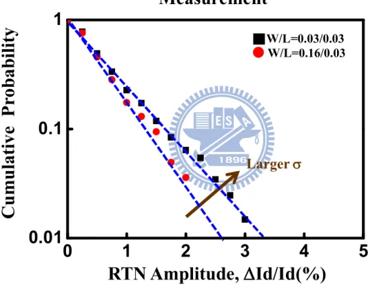
Fig. 2.2 RTN amplitude recorded with cumulative probability is distributed exponentially and smaller cell has larger .
p.9
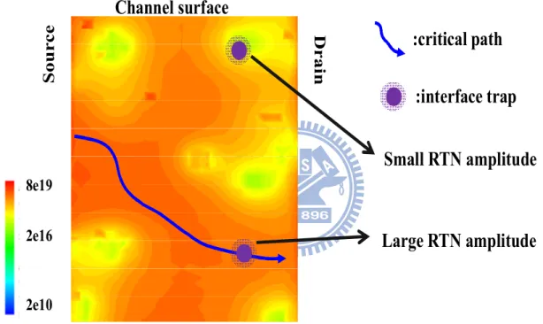
Fig. 2.3 There is a critical path that most current percolates through it. P.10
Fig. 2.4 Here is the simulation flow of computing RTN amplitude. p.11
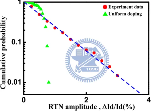
Fig. 2.5 Simulation with uniform doping does not behave like the measurement.
p.12
Fig. 2.6 (a) Substrate uniform doping cannot create percolation path. (b) Different trap position along channel length.
p.13
Fig. 2.7 Max RTN amplitude in substrate uniform doping is located in the middle of channel.
p.14
Fig. 2.8 (a) 3-D “atomistic” simulation describes RTN amplitude characteristic well.
(b) A critical path is generated by random dopants.
p.15
Fig. 2.9 (a) (W=L)-1.5
well describes the dependence of (b) W-1 is in good agreement with the simulation.
p.16
(c) Na0.3 well describes RTN amplitude characteristic.
(d) n-0.5 agrees with standard deviation property.
p.17
Fig. 2.10 RTN amplitude versus drain current (a) Measurement (b)Simulation
vi
Fig. 2.11 Percolation effect turns into number fluctuation in strong inversion from the top view of the device.
p.19
Fig. 2.12 RTN amplitude changes with different bulk voltage. p.20
Fig. 2.13 (a) Smaller RTN amplitude is observed in higher VB.
(b) Electrons are pulled away from positive VB.
p.21
Fig. 2.14 (a) Here is the top view of the channel.
(b) Electron density along channel direction is sown with different VB.
p.22
Fig. 2.15 (a) Simple sketch stands for pocket implant.
(b) Here exhibits pocket concentration dependence of .
p.23
Fig. 2.16 (a) RTN amplitude distribution is plotted without pocket along L. (b) RTN amplitude distribution is plotted with pocket along L.
p.24
Fig. 2.17 (a) RTN amplitude distribution is plotted along L. (b) RTN amplitude distribution is plotted along W.
p.25
Fig. 3.1 (a) Charges are trapped in oxide under positive gate bias. (b) Here shows typical characteristic of BTI behavior.
p.29
Fig. 3.2 Experiment data are distributed exponentially. p.30
Fig. 3.3 (a) Flow chart of BTI simulation is shown here.
(b) Here compares between measurement and simulation.
p.31
Fig. 3.4 Here exhibits (a) W=L and (b) W dependence of p.32
Fig. 3.5 (a) Threshold voltage distribution in fresh state is shown here. (b) Threshold voltage distribution in stress state is shown here.
vii
Fig. 4.1 Here plots a staircaselike evolution of a read current with retention time. p.39 Fig. 4.2 Fig. 4.3 Fig. 4.4 Fig. 4.5 Fig. 4.6 Fig. 4.7
Electrons are tunneling from nitride because of thin bottom oxide.
(a) Three Vt retention traces versus cumulative retention with two,
three, and six P/E cycles.
(b) An average of 50 retention traces follows tunneling front model.
Distribution of a single-program charge loss induced Vt is plotted
in this figure.
(a) Simulation of Vt retention loss characteristic in three cells is
shown here.
(b) An average of Vt retention loss simulations follows tunneling
front model.
Same electrons jump from nitride layer in equal time scale.
Monte-Carlo-simulated Vt retention distribution at a retention time of 103 s and 106 s. p.40 p.41 p.42 p.43 p.44 p.45
1
Chapter 1
Introduction
Due to the reduction in device geometries advances aggressively, single charge induced threshold voltage fluctuation becomes more and more important. In extreme case, multi-level-circuit might be read failure caused by several electrons loss. That’s why we focus on single charge phenomenon in this report.
2D uniform doping is not suitable because devices are getting smaller and smaller now. It is inappropriate to regard that dopants are still arranged uniformly. In some case, there are only tens of dopants in substrate region. We do have reason to believe that the position of dopants play an important role in devices’ electrical characteristic. Therefore, introduction of 3D atomistic simulation is inevitable.
There are five chapters in this report. Chapter 1 is an introduction to help readers fit in our discussion as soon as possible. Basic RTN mechanism is presented in chapter 2, we also make a prediction of single charge behavior on different dimension, doping concentration and electron density. Bulk voltage effect and pocket implant’s influence on RTN are also discussed here. In chapter 3, Bias temperature instability effect is studied. We do researches on retention loss in SONOS flash memory in chapter 4. Last but not least, our conclusion is in the last chapter.
2
Chapter 2
Discussion of RTN Characteristic
2.1 Introduction
As a result of impressive downscaling of device dimension, the cells with nanometric size only have a few dopants and driving carriers in silicon-based substrate [2.1]. It might cause multi-level-cell read failure by only several electrons trapping/detrapping. This would be a prominent issue in designing devices. Therefore, we start from the most common phenomenon, random telegraph noise, to begin our research.
In this chapter, we will simply explain the meaning of random telegraph noise (RTN), and then introduce its most important characteristic, percolation effect and number fluctuation. We would make a prediction of RTN’s influence on different device dimension, doping concentration and electron density subsequently. At last, we use our simulation result to give an explanation the effect of bulk voltage and pocket implant on RTN amplitude.
2.2 Percolation Effect and Number Fluctuation
We would like to start from introducing RTN mechanism in the beginning, as shown in Fig. 2.1, there are obvious two current level in the picture. High current level stands that the trap in oxide is empty state with smaller threshold voltage. On the contrary, low current level states that there is an electron trapped in the oxide defect causing high threshold voltage [2.2]. According to Fermi-Dirac statistics [2.3], we know that the behavior of trapping and detrapping is most probable when trap energy is close to Fermi level. There are three important parameters shown in Fig. 2.1, c, e and d. c is called
3
in oxide. e stands for emission time that we understand it as the time for the oxide defect
to emit an electron. d is the current difference between two level caused by the capture and emission of single electron. In our 3D atomistic simulation, we focus on d. Here is definition of RTN amplitude in our report:
Eq (2.1) Id stands for high current level. We use it to normalize RTN amplitude.
We do hundreds of measurement on high k CMOS and analyze our data between different dimensions. We find out two important rules in our experiment shown in Fig. 2.2. First, all dimensions follow exponential form [2.4]:
Eq (2.2) And its cumulative form:
Eq (2.3) It should be noticed that we change the parameter Vt into d with the assumption
of fixed gm for the convenience of comparing experiment data and simulation result.
Second, there is a clear separation between the two dimensions. It is obvious that the devices with smaller width get larger RTN amplitude with same probability. In other words, it can be understood that small dimension devices have larger by Eq 2.3 [2.5]. Both phenomena would be explained later.
Electrons would like to avoid substrate dopants because of their low local potential from source to drain as shown in Fig. 2.3. Therefore, there might form a path that most electrons would flow through it called critical path [2.6]. We can imagine that if the oxide trap locates at the critical path, larger RTN amplitude is predictable since more electrons
1
(
trap)
exp(
Vt
trap)
f
Vt
(
trap)
exp(
Vt
trap)
f
Vt
100%
d dI
I
4
are affected by this charge. On the contrary, smaller RTN amplitude is a result of oxide defect residing in low electron density region [2.7]. This kind of behavior that oxide traps’ location interacts with random dopants’ position determining RTN amplitude is called percolation effect.
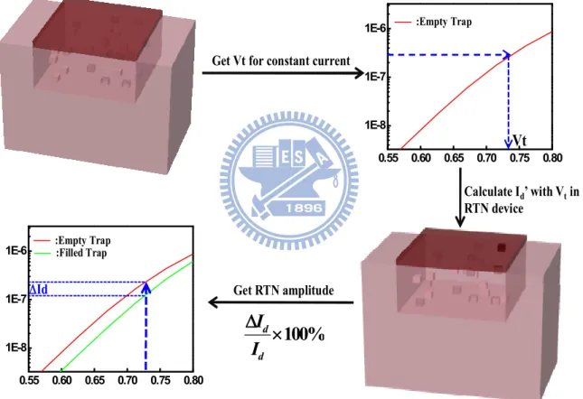
Before starting our discussion, we would like to introduce the simulation flow of RTN amplitude. Building a device including dimension and doping profile is the first thing we have to do. And then what we should do is determining a constant current to extract the threshold voltage with empty traps. We calculate Id from threshold voltage with filled state subsequently. At last, we get RTN amplitude from Eq (2.1). The full simulation process can be seen at Fig. 2.4.
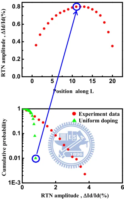
We need to know whether the atomistic doping is necessary or not, so we try to simulate RTN amplitude distribution with uniform doping. As shown in Fig. 2.5, there are huge differences between our simulation and experiment. First, it is not exponential distribution in our simulation. Second, the maximum RTN amplitude of experiment data is much larger than simulation. Uniform doping totally failed to simulate single charge’s behavior. We can find out there is no critical path in this case shown in Fig 2.6 (a). RTN amplitude seems to be merely determined by its position. It seems that RTN might be largest in the middle of channel since its coulomb force can influence most electrons. To check this phenomenon, we make traps reside in the middle of channel width, and calculate their RTN amplitude from source end to drain end as shown in Fig 2.6(b). In Fig 2.7, it can be noticed that the largest RTN amplitude really locates on the middle of channel length [2.7]. Besides, it also is the maxima value of uniform doping in Fig. 2.5. We can be told that RTN amplitude is truly controlled by defect’s location in this case. We called this kind of phenomenon number fluctuation.
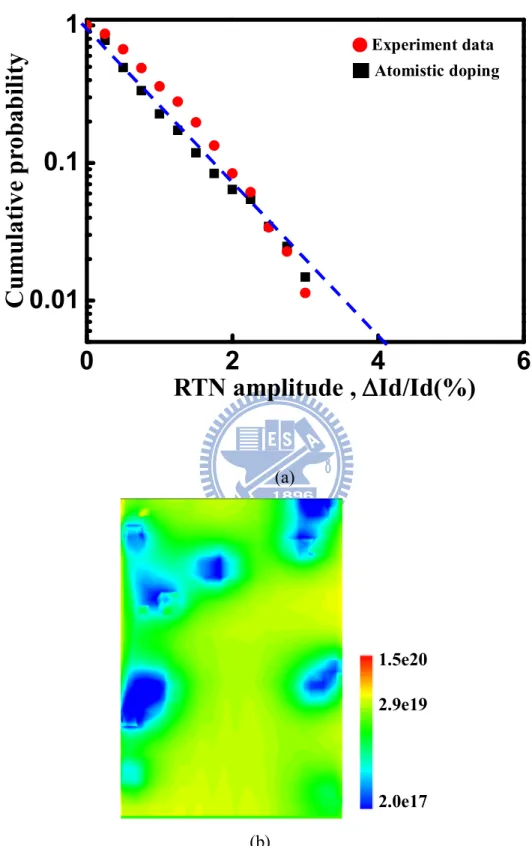
And then we use an efficient 3-D “atomistic” simulation technique to study the random dopant-induced drain current degradation [2.8], a good conformity is shown in
5
Fig 2.8(a). Both distribution and max value is in good correspondence between experiment and simulation. With inspection on the surface of channel in Fig 2.8(b), we find out there is a critical path from source to drain. It matches our assumption in percolation theory, so we believe that this simulation has its value in this report.
2.3 geometry, doping and inversion dependence of
The threshold voltage variation statistical spread, namely, , is the key point to handle random telegraph noise reliability issues for in the future technology node. An accurate prediction is very crucial, it can help us to design the programming window. It also provides the probability of overlapping to guide the design of error correction systems [2.5].
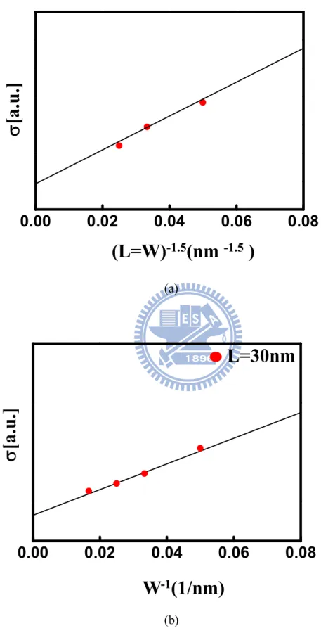
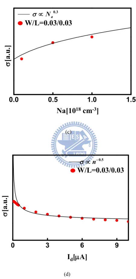
The scaling trend of RTN instabilities was investigated by applying ISE-TCAD simulation to a MOSFET device by changing channel length, channel width, doping concentration, and electron density, in the case of assuming discrete dopants randomly placed in substrate according to a uniform distribution [2.9] [2.10]. The scaling trend for assuming W=L is well described by a power-law (W=L)-1.5 as shown in Fig. 2.9(a). The dependence is stronger than the 1/(WL)0.5 dependence proposed in [2.11]. In Fig. 2.9(b), we also investigate the dependence of of W, finding out W-1 is in a good agreement with simulation result. Simulation points out that the (W=L)-1.5 can be decomposed by W-1 and L-0.5. It means that width has a stronger impact on than channel length [2.12] [2.13]. Fig. 2.9(c) shows that a larger average substrate doping results in an increase of because the possibility of obtaining larger randomness in local potential is increased by a larger number of dopants. This enhances the percolation effect which is responsible for the behavior of exponential distribution, giving rise to a 0.3 dependence of on doping concentration. Smaller is observed while electron density increases in Fig. 2.9(d)
6
because of decreasing the influence range of local potential by strong inversion. Reciprocal of square root dependence well describes the dependence of on electron density. The reason’s accuracy would be discussed in next paragraph. It should be noticed that we substitute electron density with drain current because electron density is not controllable in our simulation. We assume electron velocity is constant in different inversion condition and drain current can be treated as electron density in Eq 2.4. Here n means electron density and v represents for electron velocity.
Eq (2.4) We would like to do some discussion about the relationship between RTN amplitude and drain current. It can be seen that RTN amplitude becomes smaller when drain current increases in our experiment as shown in Fig. 2.10(a). Same phenomenon can be observed in our simulation, we also see that RTN amplitude converges gradually to a value in large drain current in Fig.2.10 (b). It is reasonable to make a hypothesis that percolation effect is dominant in small Id and number fluctuation is dominant in large Id.
Our point can be affirmed in Fig. 2.11, critical path disappears when channel is in strong inversion.
In summary, RTN scaling can be described by the following compact expression with these main cell parameters:
Eq (2.5)
2.4 V
Beffect on RTN amplitude
Since our explanation of RTN amplitude is determined by electron density affected
d
I
qnv
0.3 aN
W nL
7
by coulomb force of oxide charge. We would like to manipulate the number of electrons in channel surface. Adding VB is a method used to control the electron distribution in
substrate. Fig 2.12 shows our experiment result, smaller RTN amplitude is observed in high VB state. We get same conclusion in this simulation, a reasonable explanation is that
electrons are pulled away from channel surface by positive VB as shown in Fig. 2.13. For
getting more proof, we cut a line from source to drain to observe the variation of electron density distribution. Fig. 2.14 tells us that electron density gradually decreases while VB
becomes larger. Under the condition of fixed current, number of electrons should be constant. The only explanation of less electron density in channel surface is that they are pulled away by positive VB.
2.5 Pocket implant effect on RTN amplitude
To improve punch through phenomenon and short channel effect [2.14] [2.15], people tend to add pocket implant around source and drain. In our view, it can be regarded as high local doping concentration shown in Fig. 2.15(a). We also do the prediction with different pocket concentration like section 2.3. A similar result like before, pocket implant concentration would result in a 0.3 dependence of . Only difference is that simulation data is a little away from fitting curve as shown in Fig. 2.15(b). To investigate the effect of pocket implant, we plot position along channel length and channel width versus RTN amplitude. We can see that pocket implant make RTN amplitude much larger than before in Fig. 2.16(a) and Fig. 2.16(b). It can be attributed to larger disuniformities in channel inversion in presence of a larger number of dopants. This enhances the percolation effect which is responsible for the of RTN amplitude distribution. Fig 2.17 proves correctness of the explanation in another way, RTN amplitude along width direction remains the same whether there is pocket implant or not.
8 (a)
(b)
Fig.2.1 (a) Traps start to capture and emit electrons when ET is close to EF.
(b)A two-level drain current waveform caused by capture and emission in an oxide defects. c, e and Id present capture time, emission time and current
degradation respectively.
SiO
2Si
E
FE
vE
cE
tTime[a.u.]
D
ra
in
C
u
rr
e
n
t[a
.u
.]
Id
t
ct
eI
d9
Fig. 2.2 RTN amplitude recorded with cumulative probability is distributed exponentially and smaller cell has larger .
RTN Amplitude, Id/Id(%)
C
u
m
u
la
ti
v
e
P
ro
b
a
b
il
ity
0
1
2
3
4
5
0.01
0.1
1
W/L=0.03/0.03 W/L=0.16/0.03Measurement
Larger
10
Fig. 2.3 There is a critical path that most current percolates through it.
:interface trap
Large RTN amplitude
Small RTN amplitude
:critical path
S o u r c e D r a inChannel surface
8e19 2e10 2e1611
Fig. 2.4 Here is the simulation flow of computing RTN amplitude.
0.55 0.60 0.65 0.70 0.75 0.80 1E-8
1E-7 1E-6
Get Vt for constant current
0.55 0.60 0.65 0.70 0.75 0.80 1E-8 1E-7 1E-6 Calculate Id’ with Vtin RTN device Get RTN amplitude
100%
d dI
I
:Empty Trap :Filled Trap :Empty Trap Vt Id12
Fig. 2.5 Simulation with uniform doping does not behave like the measurement.
Uniform doping Experiment data
0
2
4
0.01
0.1
1
C
u
m
u
la
ti
v
e
p
ro
b
a
b
il
it
y
RTN amplitude , Id/Id(%)
13 (a)
(b)
Fig 2.6 (a) Substrate uniform doping cannot create percolation path. (b) Different trap position along channel length.
Source
RTN position
Drain3.3e18
9.3e19
2.7e19
14
Fig. 2.7 Max RTN amplitude in substrate uniform doping is located in the middle of channel. 0 5 10 15 20 0.0 0.2 0.4 0.6 0.8 R T N a m p li tu d e , Id /I d (% ) 0 2 4 6 1E-3 0.01 0.1 1 Uniform doping Experiment data C u m u la ti v e p ro b a b il it y RTN amplitude , Id/Id(%) Position along L
15 (a)
(b)
Fig. 2.8(a) 3-D “atomistic” simulation describes RTN amplitude characteristic well. (b) A critical path is generated by random dopants.
0
2
4
6
0.01
0.1
1
Experiment data Atomistic dopingC
u
m
u
la
ti
v
e
p
ro
b
a
b
il
it
y
RTN amplitude , Id/Id(%)
1.5e20 2.9e19 2.0e1716 (a)
(b)
Fig. 2.9 (a) (W=L)-1.5 well describes the dependence of (b) W-1 is in good agreement with the simulation.
[a
.u
.]
(L=W)
-1.5(nm
-1.5)
0.00
0.02
0.04
0.06
0.08
W
-1(1/nm)
0.00
0.02
0.04
0.06
0.08
[a
.u
.]
L=30nm
17 (c)
(d)
Fig. 2.9(c) Na0.3 well describes RTN amplitude characteristic.
(d) n-0.5 agrees with standard deviation property.
Na[10
18cm
-3]
[a
.u
.]
0.0
0.5
1.0
1.5
0.3 aN
W/L=0.03/0.03
0
3
6
9
I
d[mA]
[a
.u
.]
0.5n
W/L=0.03/0.03
18 (a)
(b)
Fig. 2.10 RTN amplitude versus drain current (a) Measurement (b)Simulation
1E-7
1E-6
Drain Current(A)
R
T
N
A
m
pl
it
u
de
,
Id/
Id[
a
.u.
]
Simulation
Percolation effect Number fluctuation1E-7
1E-6
1E-5
Average
R
T
N
A
mpli
tude
,
Id/I
d[
a
.u.
]
Drain Current(A)
19
Fig 2.11 Percolation effect dominant turns into number fluctuation dominant in strong inversion from the top view of the device.
Percolation Effect Dominant
Number Fluctuation Dominant
Strong inversion
Top View
20
Fig. 2.12 RTN amplitude changes with different bulk voltage.
4.50x10
-74.75x10
-75.00x10
-7Times[a.u.]
21 (a)
(b)
Fig. 2.13(a) Small RTN amplitude is observed in high VB.
(b) Electrons are pulled away from positive VB.
0
3
6
9
12
15
1E-3
0.01
0.1
1
C
u
m
u
la
ti
v
e
p
ro
b
a
b
il
it
y
RTN amplitude Id/Id(%)
VB=0V VB=0.5V VB=0.8VAdd V
B>0
S
D
S
D
22
(a)
(b) Fig 2.14 (a) Here is the top view of the channel.
(b) Electron density along channel direction is sown with different VB.
RTN position
8e19
2e10
2e16
E
le
c
tr
o
n
D
e
n
si
ty
(1
/c
m
3)
Channel length direction(um)
-0.02
-0.01
0.00
0.01
0.02
1E18
1E19
1E20
VB=0V VB=0.5V VB=0.8V23
(a)
(b)
Fig. 2.15(a) Simple sketch stands for pocket implant.
(b) Here exhibits pocket concentration dependence of .
P
P
N
aPocket concentration [10
18cm
-3]
[a
.u
.]
2
4
6
24 (a)
(b)
Fig. 2.16(a) RTN amplitude distribution is plotted without pocket along L. (b) RTN amplitude distribution is plotted with pocket along L. Position along L R T N a m pl it ude , Id/ Id( % )
No pocket
-20 -15 -10 -5
0
5
10
15
20
0
2
4
6
8
10
Position along L R T N a m pl it ude , Id/ Id( % )Pocket concentration:5e18
-20
-10
0
10
20
0
2
4
6
8
10
25 (a)
(b)
Fig. 2.17(a) RTN amplitude distribution is plotted along L. (b) RTN amplitude distribution is plotted along W.
Position along L
-20 -15 -10 -5
0
5
10
15
20
0
1
2
3
4
5
R
T
N
a
m
p
li
tu
d
e
,
Id
/I
d
(%
)
: No pocket: pocketPosition along W
-30
-20
-10
0
10
20
30
0
1
2
3
4
5
R
T
N
a
m
p
li
tu
d
e
,
Id
/I
d
(%
)
: No pocket : pocket26
Chapter 3
Single charge induced V
t
variation in high
COMS
3.1 Introduction
The larger, micrometer-sized FET devices were considered identical in terms of electrical performance in the past CMOS technology [3.1]. Now with the continuous scaling of transistor dimensions, the reliability degradation of circuits has become an important issue [3.2]. Besides, high-dielectric-constant (high k) materials have replaced SiO2 as gate dielectric in CMOS devices [3.3]. Due to an increasing electric field across
the oxide, the generation of interface traps under bias temperature instability (BTI) in MOS transistors has become one of the most critical reliability issues that determine the lifetime of CMOS devices [3.4] [3.5].
Now as CMOS devices scale toward atomic dimensions, device parameters become statistically distributed. We know that design of any digital circuit is based on the presumption that transistor parameters will remain bounded by a certain margin during the projected lifetime of the IC, so understanding these distributions will be important for correctly predicting the reliability of future deeply downscaled technologies [3.1].
3.2 BTI effect in high k CMOS
We would like to explain the mechanism of BTI briefly in the beginning of this section. Oxide traps generation is ascribed to breaking of SiH bonds at the SiO2/Si substrate interface by a combination of electric field, temperature, and holes [3.6]. Trap energy would be pulled down by positive gate bias, it would be more probable to be
27
trapped in oxide defects as shown in Fig. 3.1(a). To enhance transistor performance without scaling gate oxide, it is normal to increase oxide field which results in more trap energies lower than Fermi-level in same gate bias. This is one of reasons why BTI issue becomes more and more important. Fig 3.1(b) is our experiment data, it is clear that each drain current drop is different and abrupt. It implies that BTI stress induced Id might be
affected by random dopants and oxide defects as we discussed in chapter 2. Therefore, we plot our experiment data in Fig. 3.2 and find out the individual BTI relaxation steps are exponentially distributed in amplitude just like RTN behavior we discussed before. Before starting the simulation, number of stress charge in our experiment should be recorded by counting steps of drain current degradation in our stress time. The next step we need to do is making a criterion of const current to decide the threshold voltage and calculate each state’s drain current. The entire flow chart is in depicted in Fig. 3.3 (a). We would get different delta Id with each stress electron like the measurement in Fig. 3.1(b). Fig 3.3 (b)
is the comparison between measurement and simulation, it turns out that RTN amplitude distribution is in a good agreement with experiment. Both of their RTN amplitude is distributed exponentially, the fact tell us that the behavior of BTI obey percolation theory, too.
The good fitting result proves the correctness of our simulation method and makes sure the figure we provide subsequently is believable. Based on the similarity behavior between random telegraph noise and bias temperature instability, we cannot stop wondering whether other properties would like RTN or not.
In the following, we do a prediction of changing the channel length and channel width simultaneously. 20 nanometer, 30 nanometer and 40 nanometer are involved in this simulation in Fig 3.4(a). We notice that (W=L)-1.5 well describes the dependence of like RTN. With the curiosity, width dependence with fixed channel is investigated. After 20 nanometer, 30 nanometer and 60 nanometer simulation, we realize that the dependence of
28
follows the power-law in the form of W-1 in Fig. 3.3(4). It turns out that both BTI stressed induced drain current variation and geometry dependence of follows random telegraph noise mode such as exponential distribution and power law.
At last we would like to discuss the change of threshold voltage distribution caused by BTI stress. There is a small difference compared to first paragraph in section 3.2. We calculate drain current with fix threshold voltage at fresh state before and now the constant current is fixed with stressed charges in oxide defects. It could be taken for granted that threshold voltage increases in the condition of more charges trapped in oxide layers. Besides, we observe the standard deviation of threshold voltage distribution in both fresh state and stress state. Larger is obtained in the stress state as shown in Fig. 3.5, it means that there should leave more space for designing devices.
29 (a)
(b)
Fig. 3.1(a) Charges are trapped in oxide under positive gate bias. (b) Here shows typical characteristic of BTI behavior.
E
FE
vE
cSiO
2Si
E
tTime(sec)
Id[
a
.u
.]
Time(sec)
1E-4 1E-3 0.01
0.1
1
10
100
Id Fresh Id Id30
Fig. 3.2 Experiment data are distributed exponentially.
C
u
m
u
la
ti
v
e
p
ro
b
a
b
il
ity
RTN amplitude , Id/Id(%)
0
3
6
9
12
1E-3
0.01
0.1
1
31 (a)
(b)
Fig. 3.3(a) Flow chart of BTI simulation is shown here.
(b) Here compares between measurement and simulation.
0.4 0.6 0.8 :Empty Trap :1st stress :2nd stress Vg(volts) D ra in c u rr en t[ a .u .] Id1 Id2 S tr es s e le c tr o n Id -V g si m u la ti o n 0 3 6 9 12 1E-3 0.01 0.1 1
C
u
m
u
lat
ive
p
rob
ab
il
it
y
RTN amplitude , Id/Id(%)
Experiment Simulation32
(a)
(b)
Fig. 3.4 Here exhibits (a) W=L and (b) W dependence of
[a
.u
.]
0.00
0.02
0.04
0.06
0.08
(L=W)
-1.5(nm
-1.5)
[a
.u
.]
L=30nm
0.00
0.02
0.04
0.06
0.08
W
-1(1/nm)
33 (a)
(b)
Fig. 3.5(a) Threshold voltage distribution in fresh state is shown here. (b) Threshold voltage distribution in stress state is shown here.
0.88
0.92
0.96
1.00
1.04
0.0
0.1
0.2
0.3
0.4
V
t(Volt)
p
ro
b
a
b
il
ity
10% V
tvariation
:16.8mV
0.88
0.92
0.96
1.00
1.04
0.0
0.1
0.2
0.3
0.4
V
t(Volt)
p
ro
b
a
b
il
ity
10% V
tvariation
:17.3mV
34
Chapter 4
Single charge induced V
t
variation in
SONOS Flash Memory
4.1 Introduction
In recent years, the scaling of SONOS flash memory advances aggressively, as a result of tiny dimension of nitride layer, it would not be surprised that fewer program electrons can be stored. Therefore, a single charge loss might play a significant role in the reliability issue [4.1]. It can not only induce huge variation in read current but also result in a read failure. There are two main single charge phenomena in this report. One is called random telegraph noise arising from single electron emission and capture at an interface trap site discussed in chapter 2 in detail [4.2]. The other is discrete program charge retention loss caused by single charge vertical loss with the help of traps in oxide [4.3] [4.4].
The amplitude distribution of RTN in a floating gate flash memory is proven to be exponential due to percolation effect caused by random dopants in the substrate induced local potential variation [4.2], [4.5], [4.6]. We would like to investigate whether single charge loss in a SONOS flash induced threshold voltage distributes exponential or not. Understanding the behavior of retention loss is crucial for predicting the reliability of future deeply downscaled technologies.
4.2 Measurement Condition
In this section, the first thing should be investigated is the characteristic of threshold voltage variation in SONOS flash memory. To measure Vt induced by single charge loss
35
from nitride layer, our experiment decomposed into two phase: retention phase and read phase. Retention phase is used to let electron jump from traps in nitride, so there is no voltage bias in gate, source, drain and bulk. Read phase helps us to know drain current condition, drain bias is 0.1 volt and gate voltage is biased at subthreshold region to amplify the effect of retention loss. The time intervals in the retention phase and read phase are 1s and 0.1s. The SONOS devices in our experiment have 70 nanometer channel length and 80 nanometer channel width. The oxide/nitride/oxide layer thickness is 8nm, 7nm and 2.5nm, respectively. Thick bottom oxide with better retentivity is not suitable in our case [4.7]. Thinner bottom oxide can help us to collect more electrons loss from SONOS. We choose 2V as program window and achieve this goal by using Fowler-Nordheim program. By the way, FN is used in our erase, too.
4.3 Retention Loss in SONOS Flash Memory
Fig 4.1 shows a typical behavior of read current versus retention time. Abrupt jumps caused by single electron emission are clearly observed. Most convincing explanation is electrons tunneling from nitride with thin bottom oxide. Variation of threshold voltage range from several millivolt to tens of millivolt, it is reasonable to doubt that single charge loss follows percolation effect.
To obtain threshold voltage variation, we measure Vt retention in different devices
and different P/E cycles. Fig 4.3 shows Vt retention traces at a cycle number of 2, 3 and 6
which are obtained from drain current versus retention time multiplied by a subthreshold swing at read phase. It is not hard to see that single charge induced threshold voltage varies greatly from cycle to cycle. Fig 4.3(b) presents an average of 50 retention traces in ten different devices with different P/E cycles. It turns out that average Vt retention loss is
36 tunneling front model in ultra thin oxide [4.8].
Fig 4.4 plots threshold voltage variance versus cumulative probability without data point less than 10 millivolt because of the resolution of Agilent 4155c. It implies that Vt
also follows Eq 2.3. The standard deviation here is about 8 mV.
Besides, we execute a simulation with uniform doping and program charge distribution. We put a single charge in nitride layer in the center of channel length and take it away. According to Fig. 2.7, middle of channel should be the most effective position to induce threshold voltage variation. It turns out that maximum Vt in uniform doping is only about 12mV. Therefore, we attribute the extreme value of threshold voltage shift like 45mV in Fig. 4.3 to percolation effect. In other words, current percolation paths in a SONOS cell are affected by random dopants and nitride program charge [4.9].Only when the oxide traps locate at critical path would result in such a huge value.
In addition, we introduce a Mote Carlo simulation which can take both threshold voltage degradation and spread of Vt retention loss into account. Both property like
exponential distribution and tunneling front model can be seen in this simulation. Our simulation flow is described as follows. First, number of charge loss from nitride layer is counted in our measurement during retention time. By the way, program charge density calculated from number of single charge loss and nitride layer volume is 6.3e18 /cm3. In the part of simulating the time of electrons jumping out from nitride defects, we assume that traps are uniformly distributed in the nitride layer and calculate charge tunneling time of each trapped electron by tunneling front model as follows [4.10]:
Eq (4.1) 0, e are constant and x is distance from bottom oxide surface in our case.
One thing should be noticed is the range of nitride defects location. There is a limited 0
exp(
ex
)
37
deepness in nitride layer within our retention time and we call it d. Then we generate a uniformly random number r between zero and d. And we calculate corresponding charge tunneling time with the number r. This is how we determine the time that electrons jump out of the nitride layer.
At the amplitude of threshold voltage variation, we build up its behavior with calculated from measurement like Eq 4.2.
Eq (4.2) Since Eq (4.2) is a form of probability, its value must be in the interval of 0 and 1. All we need to do is create a random number p between 0and 1. This number presents the probability in Eq 4.2. Then Vt can be calculated in the condition of knowing two-thirds
parameters in Eq 4.2. Fig. 4.5(a) is combination of threshold voltage variation and retention time and Fig. 4.5(b) is an average of 100 simulation data and shows that simulated result is in good agreement with the experiment. Both of them obey tunneling front model.
4.4 Threshold Voltage Distribution Prediction
Assuming traps uniformly distributed in the nitride layer, we can infer that average threshold voltage retention loss exhibits logarithmic time dependence. As shown in Fig. 4.6, nitride trap density is proportion to charge tunneling time. In other words, we can predict the number of charge loss in the future in the same time scale. It is very useful in reliability issue. Products lifetime can be calculated with shorter period. It is not necessary to wait for devices malfunction anymore. For example, if we know that devices lost 10 electrons in 103s, then we can deuce that there is a great chance that 20 electrons would jump out of nitride layer according to tunneling front model.
, ,
(
t trap)
exp(
V
t trap)
f
V
38
In Fig 4.7, we perform the Monte Carlo analysis to a threshold voltage retention loss distribution at two retention times, namely, 103 s and 106 s. It can be observed that the standard deviation grows from 41.7mV to 62.6mV during three time scale. Threshold voltage retention loss not only shifts the whole distribution but also broaden it (increase standard deviation). It is a very bad news for flash memories, so the accuracy prediction is so important that everyone should not ignore it.
39
40
Fig. 4.2 Electrons are tunneling from nitride because of thin bottom oxide.
Source
Nitride
Drain
Oxide
41 (a)
(b)
Fig 4.3(a) Three Vt retention traces versus cumulative retention with two, three, and six P/E
cycles.
42
Fig.4.4 Distribution of a single-program charge loss induced Vt.
=8mV
Single Charge Loss Induced Vt(mV)
Cu
m
u
la
ti
v
e
p
ro
b
a
b
il
ity
10
20
30
40
50
0.01
0.1
1
43
(a)
(b)
Fig.4.5 (a) Simulation of Vt retention loss characteristic in three cells is shown here.
(b) An average of Vt retention loss simulations follows tunneling front model.
Cumulative Retention Time(sec.)
V
t
s
h
if
t(
V
)
Cumulative Retention Time(sec.)
V
tsh
if
t(
V
)
44
Fig. 4.6 Same electrons jump from nitride layer in equal time scale.
Source
Drain
X=0
45
Fig. 4.7 Monte-Carlo-simulated Vt retention distribution at a retention time of 103 s and 106 s.
V
t
Retention Loss(V)
O
c
c.
P
ro
b
a
b
il
ity
46
Chapter 5
Conclusion
In this report, a 3D atomistic simulation is used in exploring random telegraph noise in two parts, including statistic devices property and single cell characteristic. Geometry, doping concentration and electron density dependence of is discussed in first part. Then we investigate the relationship between number fluctuation and percolation effect in second part. Pocket implant and VB effect on RTN amplitude is applied to enhance the points we supply in chapter 1.
Later we discuss bias temperature instability induced current degradation and find out it follows same behavior like RTN such as percolation effect and power-law dependence of standard deviation.
At last retention loss induced threshold voltage variation is investigated in SONOS flash memory. We find out that percolation still exists here in the measurement. Prediction of threshold voltage distribution is implemented in this chapter, too.
Finally, it turns out to be all single charge induced Vt and Id variation would follows
47
Reference
Chapter 2
[2.1] Paolo Fantini, Andrea Ghetti, Andrea Marinoni, Gabriella Ghidini, Angelo Visconti and Andrea Marmiroli, “Giant Random Telegraph Signals in Nanoscale Floating-Gate Devices,” IEEE Elect. Dev. Lett. vol. 28, NO 12, 2007
[2.2] H. Lee, Y. Yoon, I. Song, and H. Shin, “FN stress induced degradation on random telegraph signal noise in deep submicron NMOSFETs,” IEICE Trans. Electron., vol. 91, pp. 776–779, 2008.
[2.3] S. M. SZE, KWOK K. NG, PHYSICS OF SEMICONDUCTOR DEVICES, THIRD EDIDTION, p17.
[2.4] Asen Asenov, Ramesh Balasubramaniam, Andrew R. Brown, and John H. Davies, “RTS Amplitudes in Decananometer MOSFETs: 3-D Simulation Study,” IEEE
Trans. Electron Devices, Vol.50, pp. 839 - 845, 2003
[2.5] A. Ghetti, M. Bonanomi, C. Monzio Compagnoni, A. Spinelli, A. Lacaita, and A. Visconti, “Physical modeling of single-trap RTS statistical distribution in Flash memories,” in Proc. IRPS Symp., 2008, pp. 610–615.
[2.6] J. P. Chiu, Y. L. Chou, H. C. Ma, T. Wang, S. H. Ku, N. K. Zou, V.Chen, W. P. Lu, K. C. Chen, and C.-Y. Lu, “Program charge effect on random telegraph noise amplitude and its device structural dependence in SONOS Flash memory,” in Proc.
IEDM Tech. Dig., 2009, pp. 843–846.
[2.7] A. Asenov, A. R. Brown, J. H. Davies, S. Kaya, and G. Slavcheva, ‘‘Simulation of Intrinsic Parameter Fluctuations in Decananometer and Nanometer-Scale MOSFETs,’’ IEEE Trans. Electron Devices 50, 1837 (2003).
[2.8] A. Asenov and S. Saini, “Suppression of random dopant induced threshold voltage fluctuations in sub-0.1 m MOSFETs with epitaxial and -doped channels,” IEEE
48
Trans. Electron Devices, vol. 46, pp. 1718–1723, 1999.
[2.9] A. Ghetti, C. Monzio Compagnoni, F. Biancardi, A. Lacaita, S. Beltrami, L. Chiavarone, A. Spinelli, and A. Visconti, “Scaling trends for random telegraph noise in deca-nanometer Flash memories,” in IEDM Tech. Dig., 2008, pp. 835–838. [2.10] A. Ghetti, C. M. Compagnoni, A. S. Spinelli, and A. Visconti, “Comprehensive
Analysis of Random Telegraph Noise Instability and Its Scaling in Deca–Nanometer Flash Memories,” IEEE T. Electron Dev., vol. 56, no. 8, pp. 1746-1752, 2009
[2.11] K. Fukuda, Y. Shimizu, K. Amemiya,M. Kamoshida, and C. Hu, “Random telegraph noise in Flash memories—Model and technology scaling,” in IEDM Tech.
Dig., 2007, pp. 169–172.
[2.12] Lu, Y.-L.R.; Yu-Ching Liao; McMahon, W.; Yung-Huei Lee; Kung, H.; Fastow, R.;
Sean Ma,” The Role of Shallow Trench Isolation on Channel Width Noise Scaling for Narrow Width CMOS and Flash Cells ” et al., in Proc. VLSI-TSA Symp., p. 85, 2008.
[2.13]Calderoni, A.; Fantini, P.; Ghetti, A.; Marmiroli, A.;,” Modeling the VTH fluctuations in nanoscale Floating Gate memories” et al., in Proc. SISPAD
Conference, p. 49, 2008.
Chapter 3
[3.1] B. Kaczer, T. Grasser, P. J. Roussel, J. Franco, R. Degraeve, L.-A. Ragnarsson, E. Simoen, G. Groeseneken, and H. Reisinger, “Origin of NBTI variability in deeply scaled pFETs,” in Proc. Int. Rel. Phys. Symp., 2010
[3.2] B. Paul, K. Kunhyuk, H. Kufluoglu, M. A. Alam, and K. Roy, “Impact of NBTI on the temporal performance degradation of digital circuits”, IEEE Elect. Dev. Lett., vol.26, p.560, 2005
49
[3.3] H. Iwai, S. Ohmi, S. Akama, C. Ohshima, A. Kikuchi, I. Kashiwagi, J. Taguchi, H. Yamamoto, J. Tonotani, Y. Kim, I. Ueda, A. Kuriyama, and Y. Yoshihara, “Advanced gate dielectric materials for sub-100 nm CMOS,” in IEDM Tech. Dig., 2002, pp. 625–628.
[3.4] N. Kimizuka, T. Yamamoto, T. Mogami, K. Yamaguchi, K. Imai, and T. Horiuchi, “Impact of bias temperature instability for direct tunneling ultrathin gate oxide on MOSFET scaling,” in Symp. VLSI Tech. Dig., 1999, pp. 73–74.
[3.5] G. Chen, M. F. Li, C. H. Ang, J. Z. Zheng, and D. L. Kwong, “Dynamic NBTI of p-MOS transistors and its impact on MOSFET scaling,” IEEE Electron Device Lett., vol. 23, no. 12, pp. 734–736, Dec. 2002.
[3.6] D. K. Schroder, “Negative bias temperature instability: What do we understand?”
Microelectron. Reliab., vol. 47, no. 6, pp. 841–852, Jun. 2007.
Chapter 4
[4.1] H. Kurata, K. Otsuga, A. Kotabe, S. Kajiyama, T. Osabe, Y. Sasago, S. Narumi, K. Tokami, S. Kamohara, and O. Tsuchiya, “The impact of random telegraph signals on the scaling of multilevel Flash memories,” in Proc. Symp. VLSI Circuits Dig., 2006, pp. 112–113.
[4.2] A. Asenov, R. Balasubramaniam, A. R. Brown, and J. H. Davies, “RTS amplitudes in decananometer MOSFETs: 3-D simulation study,” IEEE Trans. Electron Devices, vol. 50, no. 3, pp. 839–845, Mar. 2003.
[4.3] S. H. Gu, C. W. Li, T. Wang, W. P. Lu, K. C. Chen, J. Ku, and C. Y. Lu, “Read current instability arising from random telegraph noise in localized storage, multi-level SONOS Flash memory,” in IEDM Tech. Dig., 2006, pp. 487–490. [4.4] K. Fukuda, Y. Shimizu, K. Amemiya, M. Kamoshida, and C. Hu, “Random
50
Dig., 2007, pp. 169–172.
[4.5] A. Ghetti, C. M. Compagnoni, F. Biancardi, A. L. Lacaita, S. Beltrami, L. Chiavarone, A. S. Spinelli, and A. Visconti, “Scaling trends for random telegraph noise in deca-nanometer Flash memories,” in IEDM Tech. Dig., 2008, pp. 835–838. [4.6] T. Wang, W. J. Tsai, S. H. Gu, C. T. Chan, C. C. Yeh, N. K. Zous, T. C. Lu, S. Pan,
and C. Y. Lu, “Reliability models of data retention and read-disturb in 2-bit nitride storage flash memory cells,” in IEDM Tech. Dig., Washington, DC, Dec. 2003. [4.7]Y. Wang and M. H. White, “An analytical retention model for SONOS nonvolatile
memory devices in the excess electron state,” Solid State Electron., vol. 49, no. 1, pp. 97–107, Jan. 2005.
[4.8] H. C. Ma, Y. L. Chou, J. P. Chiu, T. Wang, S. H. Ku, N. K. Zou, V. Chen, W. P. Lu, K. C. Chen, and C.-Y. Lu, “Program trapped charge effect on random telegraph noise amplitude in a planar SONOS Flash memory cell,” IEEE Electron Device
Lett., vol. 30, no. 11, pp. 1188–1190, Nov. 2009.
[4.9] D. Dumin and J. Maddux,” Correlation of stress-induced leakage current in thin oxides with trap generation inside the oxides”, IEEE Trans. Electron Devices, 40, 986 (1993).