國 立 交 通 大 學
電子工程學系 電子研究所碩士班
碩 士 論 文
射頻金氧半電晶體小訊號等效電路模型參數
萃取方法建立以應用於各種偏壓與幾何結構
RF MOSFET Small Signal Equivalent Circuit
Model Parameter Extraction for Various Biases
and Geometries
研 究 生:陳冠旭
指導教授:郭治群 博士
射頻金氧半電晶體小訊號等效電路模型參數萃取方法建立
以應用於各種偏壓與幾何結構
RF MOSFET Small Signal Equivalent Circuit Model
Parameter Extraction for Various Biases and Geometries
研究生:陳冠旭 Student : Kuan-Hsu Chen
指導教授:郭治群 博士 Advisor : Dr. Jyh-Chyurn Guo
國 立 交 通 大 學
電子工程學系 電子研究所
碩 士 論 文
A Thesis
Submitted to Department of Electronics Engineering & Institute of Electronics College of Electrical and Computer Engineering
National Chiao Tung University in partial Fulfillment of the Requirements
for the Degree of Master In
Electronics Engineering August 2008
Hsinchu, Taiwan, Republic of China
射頻金氧半電晶體小訊號等效電路模型參數萃取方法
建立以應用於各種偏壓與幾何結構
研 究 生 : 陳 冠 旭 指 導 教 授 : 郭 治 群 博 士
國立交通大學
電子工程學系 電子研究所
摘要
在本論文中,發展了小訊號等效電路模型及其所對應的參數萃取方法,以應用於射 頻互補式金氧半場效電晶體電路模擬上。本研究涵蓋雙埠三端點與四埠四端點的射頻金 氧半電晶體。前者即三端點共源組態射頻金氧半電晶體是在電路設計上最為廣泛使用的 元件,為了符合雙埠射頻量測系統,其測試元件佈局必須設計成源極與基極連接在一起 並接地的雙埠組態結構。事實上,在射頻電路設計中,源極與基極並非總是連接在一起, 此傳統的雙埠測試元件將無法得到完整的四端點金氧半電晶體的特點,也無法代表正確 之高頻特性。為了解決此關鍵的問題,本研究設計四埠四端點的射頻金氧半電晶體,並 利用 0.13um 互補式金氧半場效電晶體製程研製出來探討元件高頻特性及模型的發展。 本論文中,首先介紹了雙埠與多埠散射參數(S 參數)的基本原理,然後,對於雙埠 三端點的元件,分別詳盡探討在不同的偏壓條件與幾何結構上的小訊號電路與其所對應 的參數萃取方法。基於雙埠三端元件已做的工作上,適時地改良其小訊號電路以相對應 於四埠四端點的元件架構,並建立四埠四端點的去寄生效應方法與參數的萃取流程等基 本的研究工作。 最後,在不同偏壓下所提出的小訊號等效電路分別透過模擬做更廣泛的驗證,驗證其模型的準確性以可靠地應用在超過 40GHz 的寬頻範圍,以及不同的偏壓條件如線性 區與飽和區。更重要地,所建立的等效電路模型其本身的參數值充分表現出良好的可伸 縮性,可預測於固定指叉寬度下變化閘極長度與閘極指叉數目之效應。在各種頻率、偏 壓下的準確性和元件幾何參數之可伸縮性,可有效提昇高頻電路的模擬的準確性,以及 輔助射頻互補式金氧半場效電晶體積體電路設計。
RF MOSFET Small Signal Equivalent Circuit Model
Parameter Extraction for Various Biases and Geometries
Student : Kuan-Hsu Chen Advisor : Dr. Jyh-Chyurn Guo
Department of Electronics Engineering Institute of Electronics
National Chiao Tung University
ABSTRACT
Small signal equivalent circuit models and the corresponding parameter extraction methods have been developed in this thesis for RF CMOS circuit simulation. Both two-port 3-terminal (3T) and four-port 4-terminal (4T) RF MOSFETs are covered in this work. The former one – 3T MOSFETs with a common source topology is a conventional one widely used in RF circuits, and the test-key layout is arranged in a two-port configuration with a common ground for source and body tied together to fit the two-port RF measurement system. In fact, source and body terminals are not always connected together in the practice of RF circuit design, the traditional two-port test-key cannot capture a whole spectrum of 4T MOSFET’s features and cannot adequately represent 4T MOSFET’s characteristics over high frequencies. To solve this critical problem, the latter one – four-port 4T RF MOSFETs are designed and fabricated in 0.13um RF CMOS process for high frequency characterization and model development in this work.
In this thesis, the basic principles of two-port and multi-port scattering parameters (S-parameters) will be reviewed in the first place. Then, the small signal equivalent circuits and parameter extraction methods developed for two-port 3T device under various biases and geometries will be discussed in detail. Based on what have been done for two-port 3T MOSFET, a modified equivalent circuit relevant to four-port 4T test structures, and the corresponding fundamental works, such as de-embedding method and parameter extraction
flow have been carried out.
Finally, an extensive verification has been performed on the proposed small signal equivalent circuit models through simulation under various biases. The model accuracy is certified over a broad frequency up to 40GHz and various bias conditions – linear and saturation. More importantly, the model parameters of the developed equivalent circuit models manifest themselves a promisingly good scalability over various geometries in MOSFETs, such as gate lengths and gate finger numbers under a specified finger width. The accuracy over frequencies and biases and scalability over device geometries is useful to improve accuracy of high frequency circuit simulation and facilitate RF CMOS integrated circuit development.
誌謝
時間真的過的很快,眼看碩士班生活即將結束,回想在這段時間內生活的點點滴 滴,有許多的人都必須要好好地感謝。首先我要感謝我的指導老師 郭治群教授,在研 究工作上的指導和督促,以及不斷地替實驗室成員尋求研究資源與實驗設備,讓我們不 必擔心所需的研究量測資料。在這過程中,除了讓我得到此研究領域的觀念,也體會到 更多與人相處的方法,和工作的責任感、研究態度、時間的掌控性,相信對於日後工作 或生活上會有好的幫助。 此外,還要感謝 NDL 的研究員 黃國威博士,在研究設備上的支持,讓我能夠學習 到高頻量測,也感謝 RFIC 的工程師們教導我更多量測上的觀念與指導,讓我對於量測 系統有更深的了解。也感謝高頻奈米實驗室的所有成員,益民、致廷學長,對於剛進入 實驗室的我悉心指導,也感謝仁嘉、依修、國良、等學弟以及更多的默默英雄,感謝在 你們在這段時間的陪伴,讓實驗室生活更加的豐富與有趣,不至於太苦悶。 最後,要感謝默默在我背後支持的家人,能夠提供我生活上的幫助以及養育之恩, 在我無助失落的時候給予更多的信心與鼓勵,感謝家人的全面支持,讓我能夠完成我的 碩士學位。Contents
Chinese Abstract………..i English Abstract………..iii Acknowledgement……….. v Contents………vi Figure Captions………..ix Table Captions………...xiii Chapter 1 Introduction……….1 1.1 Research motivation………1 1.2 Overview………..2Chapter 2 Fundamental theory and RF MOSFET design ………4
2.1 Non-quasi-statistic (NQS) effect……….4
2.1.1 Quasi-static (QS) model………4
2.1.2 NQS model………4
2.2 Scattering parameters………6
2.2.1 Two-port network parameters conversion………6
2.2.2 Four-port scattering parameters………7
2.2.3 Port reduction method in S-parameters………7
2.3 RF MOSFET design………8
Chapter 3 Two-port 3T RF MOSFET Model Parameter Extraction………10
3.1 De-embedding methods and verification………..10
3.1.1 Open de-embedding………10
3.1.2 Short de-embedding………11
3.2.1 Parasitic RL extraction from short pad………..12
3.2.2 Parasitic RL extraction from device………...13
3.2.3 Frequency and bias dependence of Parasitic RL………14
3.2.4 Device geometry dependence……….16
3.3 Extraction of device parameters in linear region………...17
3.3.1 Capacitance extraction and analysis………17
3.3.2 Capacitance bias and geometry dependence……….18
3.3.3 Channel resistance extraction and analysis………19
3.3.4 Substrate resistance extraction and analysis……….19
3.4 Extraction of intrinsic parameters in saturation region………..20
3.4.1 Capacitance extraction and analysis……….21
Chapter 4 Four-port RF MOSFET Model Parameter Extraction………..38
4.1 De-embedding methods………38
4.1.1 Open and Short de-embedding method………39
4.2 Parasitic RL extraction from short pad………..40
4.3 Extraction and analysis of parameters in linear region………...40
4.3.1 Extraction of parameters in linear region………41
4.3.2 Analysis of parameters in linear region……….43
4.4 Extraction and analysis of parameters in saturation region………44
4.4.1 Extraction of parameters in saturation region………44
4.4.2 Analysis of parameters in saturation region……….44
Chapter 5 Model Verification by Circuit Simulation………56
5.1 Equivalent Circuit model verification……….56
5.2 Two port 3T MOSFETs under various bias conditions……….56
5.2.1 3T MOSFETs in linear region ………..56
5.3 Four port MOSFETs under various bias conditions………...60
5.3.1 4T MOSFETs in linear region………...60
5.3.2 4T MOSFETs in saturation region………62
Chapter 6 Conclusions and Future Work……….85
6.1 Conclusions………..85
6.2 Future Work……….85
6.2.1 Parasitic resistance extraction………...85
6.2.2 Substrate resistance extraction………...85
6.2.3 Small signal equivalent circuit with body biase………...86
Figure Captions
Chapter2
Fig. 2.1 Quasi-static model assumption………. .……….9
Fig. 2.2 Input signals and the channel charge response……….9
Fig. 2.3 Quasi-Static and Non-Quasi-Static models for SPICE analysis……….9
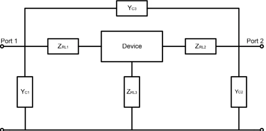
Chapter3 Fig. 3.1 The equivalent circuit of 3T device with pad………. …………22
Fig. 3.2 The equivalent circuit of open pad………. …..22
Fig. 3.3 The equivalent circuit of short pad………..22
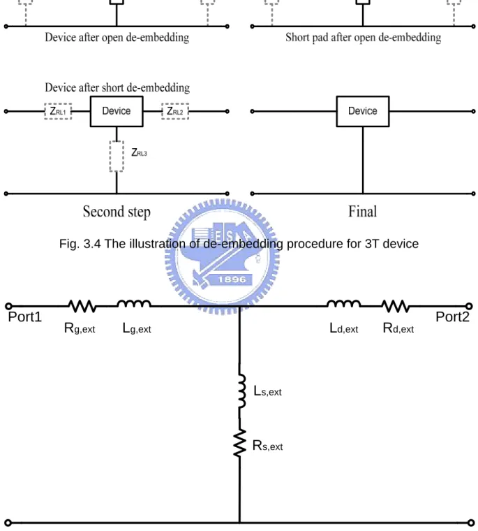
Fig. 3.4 The illustration of de-embedding procedure for 3T device………..23
Fig. 3.5 The equivalent circuit of short pad after open de-embedding………..23
Fig. 3.6 The equivalent circuit of 3T device at Vgs>>Vth, Vds=0V (Open_de) ………….24
Fig. 3.7 linear regression of optimized RG versus (Vgs -Vth)-1 at Vds=0V……….24
Fig. 3.8 linear regression of optimized RD versus (Vgs -Vth)-1 atVds=0V………..25
Fig. 3.9 The gate resistance optimized RG versus channel length at Vds=0V……...25
Fig. 3.10 linear regression of Rg_poly versus reciprocal of NFat Vds=0V………...26
Fig. 3.11 linear regression of Rd_poly versus reciprocal of NFat Vds=0V………...26
Fig. 3.12 linear regression of Rg_bias versus reciprocal of NFat Vds=0V………..27
Fig. 3.13 linear regression of Rd_bias versus reciprocal of NFat Vds=0V………..27
Fig. 3.14 channel length dependence of Rg_polyat Vds=0V………..28
Fig. 3.15 channel length dependence of Rg_chat Vds=0V………..28
Fig. 3.16 The equivalent circuit of 3T device at Vgs=Vds=0V (Open_de)………..29
Fig. 3.17 The equivalent circuit of 3T device at Vgs=Vds=0V (Open+Short_de)…….…..29
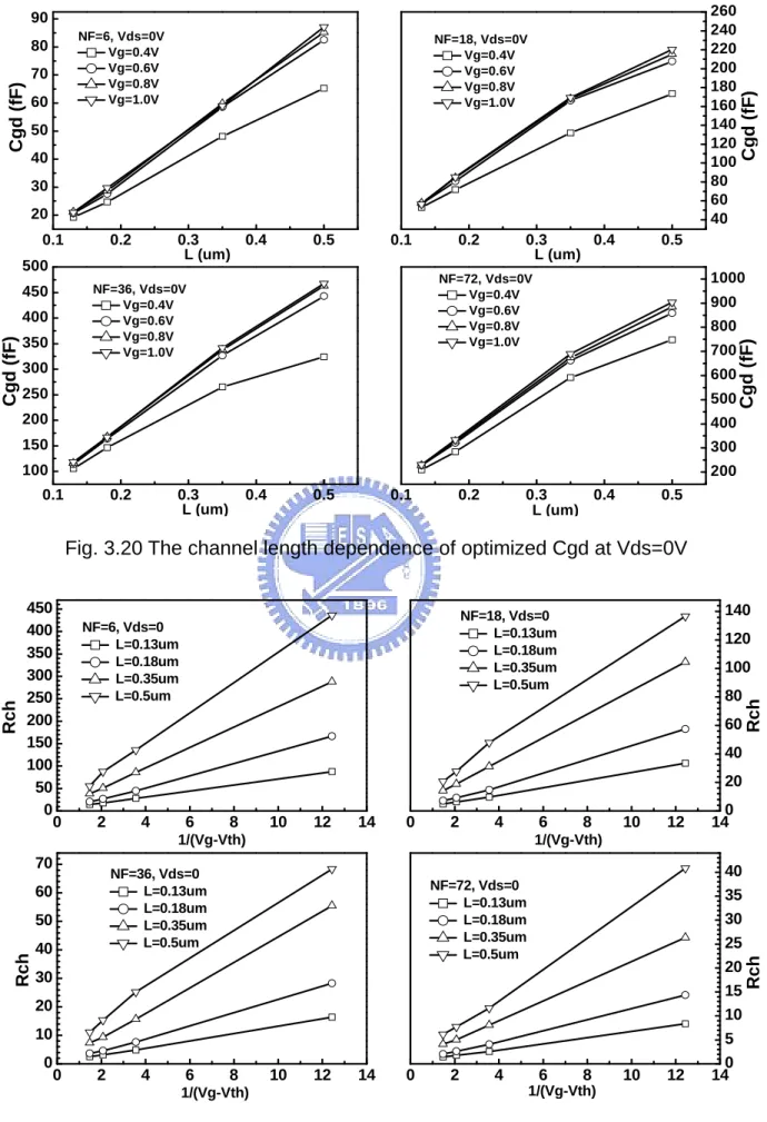
Fig. 3.19 The NF dependence of optimized Cgd at Vds=0V……….30
Fig. 3.20 The channel length dependence of optimized Cgd at Vds=0V………31
Fig. 3.21 The bias dependence of optimized Rch at Vds=0V………...31
Fig. 3.22 The NF dependence of optimized Rch at Vds=0V………...32
Fig. 3.23 The L dependence of optimized Rch at Vds=0V………..32
Fig. 3.24 The NF dependence of optimized Cjd at Vds=0V………..33
Fig. 3.25 The NF dependence of optimized Rbulk at Vds=0V………..33
Fig. 3.26 The equivalent circuit of 3T device at Vgs=Vds=1V (Open_de)………34
Fig. 3.27 Bias dependence of optimized Cgs at Vds=1V………...34
Fig. 3.28 Bias dependence of optimized Cgd at Vds=1V………35
Fig. 3.29 NF dependence of optimized Cgs at Vds=1V………35
Fig. 3.30 NF dependence of optimized Cgd at Vds=1V………36
Fig. 3.31 L dependence of optimized Cgs at Vds=1V………36
Fig. 3.32 L dependence of extracted Cgd at Vds=1V………....37
Chapter4 Fig. 4.1 The cross section and structure of four port MOSFET……….………..46
Fig. 4.2 Four port dummy open structure (M1)………..46
Fig. 4.3 Four port dummy short structure (M3)………..47
Fig. 4.4 The equivalent circuit of short pad after open de-embedding……….………47
Fig. 4.5 The equivalent circuit of four-port device at Vgs=Vds=0V………48
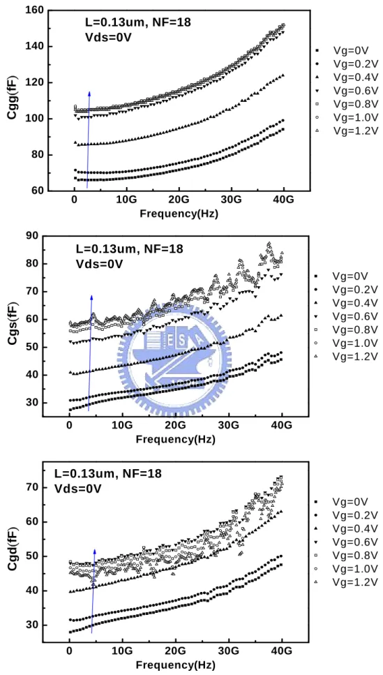
Fig. 4.6 The equivalent circuit of four-port device at Vgs=1.2V, Vds=0V (Open_de) …48 Fig. 4.7 The extracted Cgg, Cgs , Cgd capacitance verse frequency at Vds=0V…………49
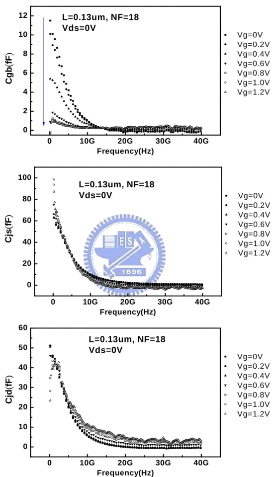
Fig. 4.8 The extracted Cgb, Cjs, Cjd capacitance verse frequency at Vds=0V………….50
Fig. 4.9 The NF dependence of optimized gate capacitances at Vds=0V……….……..51
Fig. 4.11 The NF dependence of optimized RG and Rch at Vds=0V………. …..52
Fig. 4.12 The equivalent circuit of 4-port device at Vgs=Vds=1.2V (Open_de) …….……52
Fig. 4.13 The extracted Cgg, Cgs,Cgd capacitance verse frequency at Vds=1.2V..……53
Fig. 4.14 The extracted Cgb, Cjs, Cjd capacitance verse frequency at Vds=1.2V…..……54
Fig. 4.15 The NF dependence of optimized gate capacitances at Vgs=1.2V………..…55
Fig. 4.16 The NF dependence of optimized junction capacitances at Vgs=1.2V………55
Chapter5
Fig. 5.1 The comparison of 3T devices at Vgs=Vds=0V and L=0.13um………64
Fig. 5.2 The comparison of 3T devices at Vgs>>Vth, Vds=0V and L=0.13um………..65
Fig. 5.3 The comparison of 3T devices at Vgs>>Vth, Vds=1V and L=0.13um………66
Fig. 5.4 The modified equivalent circuit of 4-port device at Vgs=Vds=0V………67
Fig. 5.5 The modified equivalent circuit of 4-port device at Vgs=1.2V, Vds=0V………67
Fig. 5.6 The measured and simulated Mag(S) of 4-port devices at Vgs=Vds=0V…69 Fig. 5.7 The measured and simulated Phase(S) of 4-port devices at Vgs=Vds=0V…70 Fig. 5.8 The measured and simulated Re(Y) of 4-port devices at Vgs=Vds=0V……71 Fig. 5.9 The measured and simulated Im(Y) of 4-port devices at Vgs=Vds=0V……73 Fig. 5.10 The measured and simulated Mag(S) of 4-port devices at Vgs=1.2V, Vds=0V………74 Fig. 5.11 The measured and simulated Phase(S) of 4-port devices at Vgs=1.2V, Vds=0V………75 Fig. 5.12 The measured and simulated Re(Y) of 4-port devices at Vgs=1.2V, Vds=0V………77 Fig. 5.13 The measured and simulated Im(Y) of 4-port devices at Vgs=1.2V, Vds=0V………78
Fig. 5. 15 The measured and simulated Mag(S) of 4-port devices at Vgs=Vds=1.2V ………80 Fig. 5.16 The measured and simulated Phase(S) of 4-port devices at Vgs=Vds=1.2V ………82 Fig. 5.17 The measured and simulated Re(Y) of 4-port devices at Vgs=Vds=1.2V ………83 Fig. 5.18 The measured and simulated Im(Y) of 4-port devices at Vgs=Vds=1.2V ………84
Table Captions
Chapter2
Table 2.1 The device geometries of two-port 3T MOSFETs………9
Table 2.2 The device geometries of four-port MOSFETs………9
Chapter3 Table 3.1 The extracted extrinsic resistance and inductance of short pad………13
Chapter5 Table 5.1 The optimized parameters for 3T device atVgs=Vds=0V………57
Table 5.2 The optimized parameters for 3T device at Vgs=1V, Vds=0V………58
Table 5.3 The optimized parameters for 3T device at Vgs= Vds=1V………..59
Table 5.4 The optimized parameters for four-port device at Vgs= Vds=0V……….61
Table 5.5 The optimized parameters for four-port device at Vgs=1.2V, Vds=0V………61
Chapter 1
Introduction
1.1 Research motivation
In the area of RF MOSFET modeling, many interesting and challenging effects have to be considered and implemented to achieve the desired accuracy and scalability. Among them, it still is a challenge in the gate resistance and substrate networks modeling and parameters extraction. It has been known that gate resistance is a primary source of the input impedance in an intrinsic MOSFET and the induced excess noise will increase the thermal noise proportional to frequency. In a
conventional approach, Rg is assumed as a constant to simplify the model formulation.
However, this assumption and the simplified model are no longer valid for simulating devices with various gate lengths in which poly sheet resistance and channel
resistance play a trade-off to each other in determining Rg. In this thesis, an improved
model is developed considering the feature of distributed TML and non-quasi-static effect in the poly gate and conduction channel. This enhancement can help improve simulation accuracy over a wide range of gate lengths.
As for substrate resistance existing in 4T devices like MOSFETs, it significantly affects the small-signal output characteristics over high frequencies and should be taken into the model for an accurate simulation, particularly under body biasing conditions. A simple substrate RC network adopting a single resistance is frequently used and the accuracy was demonstrated to around 10 GHz. However, the simplified model may lead to tremendous deviation over higher frequencies above 10 GHz and cannot fit RF circuit simulation and design using 4T MOSFET with body biases. As a matter fact, the development of an accurate substrate network model relies on the
four-port S-parameters, which cannot be achieved from conventionally used 3T devices in a two-port test structure. In other words, a reliable substrate network model and four-port 4T test structures depends on each other. In this study, four-port test structures were designed and implemented for four-port S-parameters measurement and model parameter extraction. Note that the supply voltage on each terminals can be independently controlled and a dynamic body biasing scheme can be realized in this scheme.
Based on the mentioned principles and objectives, small signal equivalent circuit models were developed and implemented in this work for three operation conditions, such as off-state, linear, and saturation regions. De-embedding and model parameter extraction methods were implemented and performed on two-port 3T and four-port 4T test structures. The model accuracy was verified through circuit simulation using ADS and comparison with S- and Y-parameters measured from multi-finger RF MOSFETs with various geometries (gate lengths, finger numbers, and finger widths). In the following, the major subject in each chapter will be described.
1.2 Overview
The main objective of this thesis is the development of small signal equivalent circuit models for RF MOSFETs and circuit simulation. This thesis is organized into six chapters as follows:
Chapter 2 provides the introduction to the non-quasi-statistic (NQS) effect for gate resistance in long channel devices and the NQS modeling in SPICE simulation. Two-port and four-port S-parameters, as well as port reduction methods for four-port to two-port will be covered in this chapter.
under different biasing conditions for two-port 3T and four-port 4T MOSFETs, respectively. The model parameters for both intrinsic and extrinsic components will be extracted under appropriate bias conditions. Then, an analysis will be performed on the extracted model parameters in the features under various biases and scalability over different geometries.
In chapter 5, the proposed equivalent circuit models will be verified through ADS simulation. It can be proven that the substrate network extracted from four-port 4T test structures can provide sufficient data base in terms of four-port S- and Y-parameters and facilitate the model accuracy for simulation under body biases.
Chapter 2
Fundamental theory and RF MOSFET design
2.1 Non-quasi-statistic (NQS) effect
As the improvement of RF CMOS technology, the cut-off frequency is roughly inversely proportional to the gate length. In the longer channel devices, the channel charge relaxation time is finite, and then, the carries in the channel can not response to the signal immediately. NQS effect should be included for the equivalent circuit model to describe the device behavior accurately over a broad frequency.
2.1.1 Quasi-static (QS) model
In Quasi-static model, the channel charge is assumed to be a unique function of the instantaneous biases, the charges per unit area at any time are assumed to identical at any position. QS model assumption is described in Fig. 2.1, the gate capacitances are lumped into the intrinsic source and drain nodes, the signal form gate will couple to source and drain side directly, this model ignores that the charge built up in the center portion of the channel does not follow a change of gate biases as readily as at the source or drain edge of channel.
2.1.2 NQS model
It has been known that the carriers in the channel can not respond to the signal immediately nearly cut-off frequency, for long channel devices, the channel transit time is roughly inversely proportional to (Vgs-Vth) and proportional to square of channel length, NQS effect become pronounced in the application, considering the
input signal with rapid rise and fall times comparable to the channel transit time in Fig. 2.2, the channel charge is not a unique function of the instantaneous terminal voltage but a function of the history of the voltage, owing to the existence of the NQS effect, QS model will be not suit to the characteristic of devices with NQS effect at the operating frequency accurately.
The method to model NQS effect for RF application, one solution is to represent the channel as n transistors in series, this model wastes on the expense of simulation time but the behavior is accurately. One solution is the RC network approach, NQS model in BSIM3v3.2.2 was based on the circuit of Elmore model, the Elmore equivalent circuit can be viewed as a first step toward an NQS model, the channel charge buildup is modeled with reasonable accuracy because it retains the lowest frequency pole of the original RC network. Fig. 2.3 illustrates the QS and NQS equivalent circuit for SPICE simulation.
The Elmore resistance RElmore is calculated from the channel resistance in strong
inversion as gst ox eff eff eff ch eff eff Elomore V C W L Rch Q e L R
μ
μ
~ 2 ∝ = (2.1)Where e is the Elmore constant with a theoretical value close to 5 and Qch is the total charge in the channel, this formulation is only valid above threshold where the
drift current dominates. The overall relaxation time τ is model as two components: τdrift
and τdiff. In strong inversion region, τdrift is dominates ; in subthreshold region, τdiff is
dominates, the relaxation time τ can be written as follows:
drift diff
τ
τ
τ
1
1
1
=
+
(2.2) wheregst eff eff ox Elmore drift
V
L
L
W
C
R
μ
τ
=
~
2 (2.3) KT qLeff diff 0 2 16μ τ = (2.4)2.2 Scattering parameters
At microwave frequency the Z, Y and H parameters are very difficult to measure, the reason is that short and open circuits to ac signals are difficult to implement at microwave frequencies, so that, the scattering matrix are used usually in the analysis of two port networks usually.
Considering the two-port network with incident wave a1 and reflected wave b1 at port1, and incident wave a2 and reflected wave b2 at port 2, the S parameters can be written in matrix form as:
⎥ ⎦ ⎤ ⎢ ⎣ ⎡ ⎥ ⎦ ⎤ ⎢ ⎣ ⎡ = ⎥ ⎦ ⎤ ⎢ ⎣ ⎡ 2 1 22 21 12 11 2 1 a a S S S S b b (2.5)
2.2.1 Two-port network parameters conversion
At a given frequency, a two-port network can be described in terms of several parameters. Therefore, there is a conversion relationship between the parameters, for example, the conversion relation between the S and Z parameters can be shown as:
[ ] [ ] [ ] [ ] [ ]
S =( Z + Z0 )−1( Z − Z0 ) (2.6)[ ] [ ] [ ] [ ] [ ] [ ]
1 0 (1 )(1 ) − − + = Z S S Z (2.7)where is the characteristic impedance diagonal matrix, and
[
is the unitdiagonal matrix. The other conversions among the Z, Y, H, and S parameters also be included in the ADS and ICCAP for using, they are useful to analyze the small signal
[
Z0]
equivalent circuit.
]
2.2.2 Four-port
k is simple, the transmission lines ⎥ ⎥ ⎥ ⎥ ⎦ ⎢ ⎢ ⎢ ⎢ ⎣ ⎥ ⎥ ⎥ ⎥ ⎦ ⎢ ⎢ ⎢ ⎢ ⎣ = ⎥ ⎥ ⎥ ⎥ ⎦ ⎢ ⎢ ⎢ ⎢ ⎣ 4 3 2 44 43 42 41 34 33 32 31 24 23 22 21 4 3 2 a a a S S S S S S S S S S S S b b b ;
scattering parameters
or The extension of the formulation to four-port netware assumed to be lossless with characteristic impedance Z0, and then, we can
write the scattering parameters of the four-port in matrix form
⎤ ⎡ ⎤ ⎡ ⎤ ⎡b1 S11 S12 S13 S14 a1
[ ] [ ][ ]
b = S a (2.8)Note that the value of S11 in (2.8) will be different from the value of S11 in a two-
port common source configuration. For example, S11 can be arranged form the S
matrix in (2.8) as 0 4 3 2 11
1
1
= = ==
a a aa
b
S
(2.9)To measure S11, the matched resistive terminations of 50Ω are used at ports 2, 3,
and
2.2.3 Port reduction method in S-parameters
of the extrinsic and intrin
(2.10)
4, and the ratio b1/a1 is obtained. In a two-port common source configuration, S11
is measured with reference resistance 50Ω at port 2 and source/body grounding.
Similarly, the parameters S12, S21, and S22 in four-port S matrix will be different form
the parameters in two-port matrix.
Considering a 4-port networks system, the I-V relationship sic parameters can be written as a 4X4 Y matrix
⎤ ⎡ ⎤ ⎡ ⎤ ⎡I1 Y11 Y12 Y13 Y14 V ⎥ ⎥ ⎥ ⎥ ⎦ ⎢ ⎢ ⎢ ⎢ ⎣ ⎥ ⎥ ⎥ ⎥ ⎦ ⎢ ⎢ ⎢ ⎢ ⎣ = ⎥ ⎥ ⎥ ⎥ ⎦ ⎢ ⎢ ⎢ ⎢ ⎣ 4 3 2 1 44 43 42 41 34 33 32 31 24 23 22 21 4 3 2 V V V Y Y Y Y Y Y Y Y Y Y Y Y I I I
According to equation (2.10), grounding a terminal is simply giving the
corresponding zero supply volt d su
representing the resulting configuration of the MOSFET, therefore, the 4 x 4 matrix of the 4-port networks can be reduced
negligible, the reduced
⎦ ⎣ ⎦ ⎣ ⎦ ⎣I Y Y V
matrix can be obtained by setting the corresponding supply voltage to zero.
2.3 RF MOSFET design
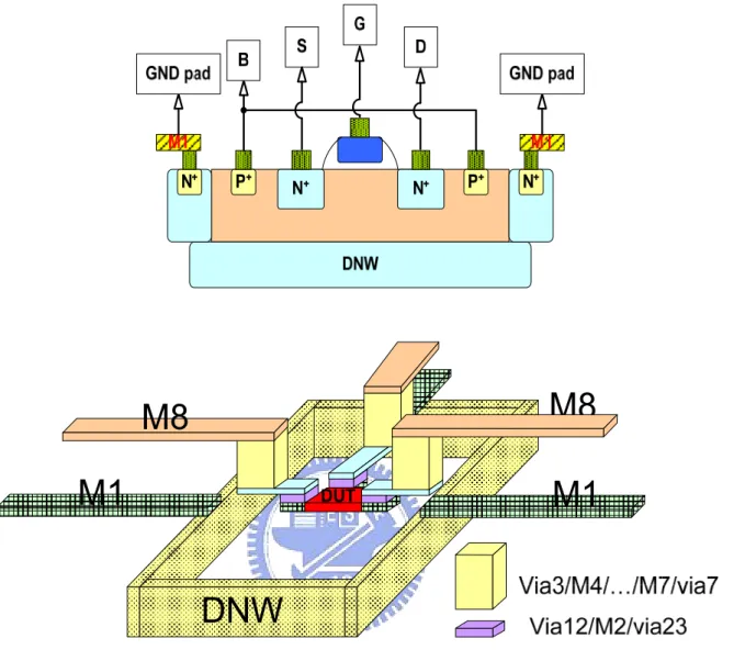
the measured S parameters are nditions and geometries, both two-port 3T and four-port 4T
Table 2.1 The device geometries of two-port 3T MOSFETs
age, and the remaine b-matrix will be the Y matrix
to 3-port or 2-port Y matrix.
For example, the common source(CS) configuration is source (port3) and body (port4) grounding, the CS 2-port Y matrix can be obtained by setting the Vs=Vb=0V in the 4-port measurement, in this case, the term of source and body in (2.10) is
Y matrix can be written as
⎥ ⎤ ⎢ ⎡ ⎥ ⎤ ⎢ ⎡ = ⎥ ⎤ ⎢ ⎡ 2 1 22 21 12 11 2 1 Y Y V I (2.11)
Similarly, the common gate and common drain Y
To understand the dependency of device parameters, and develop better scaling RF model at high frequency, the extraction from
presented under various bias co
RF MOSFETs are covered in this work. In this study, four-port S parameter measurement is supported by Radio Frequency Technology Center of National Nano Device Laboratory (NDL RFIC). The device geometries of two-port 3T and four-port 4T MOSFETs are listed in Table. 2.1 and Table 2.2, respectively.
0.13 4 6,18,36,72 L(um) W(um) NF 0.18 4 6,18,36,72 0.35 4 6,18,36,72 Dummy Pad open short 0.5 4 6,18,36,72
Table 2.2 The device geometries of four-port MOSFETs L W NF 0.13 4 6 open NF=6 short NF=6 0.13 4 18 open NF=18 Dummy Pad short NF=3 0.13 4 36 open NF=36 6
Fig. 2.1 Quasi-static model assumption
Fig. 2.2 Input signals and the channel charge response
Chapter 3
Two-port 3T RF MOSFET Model Parameter Extraction
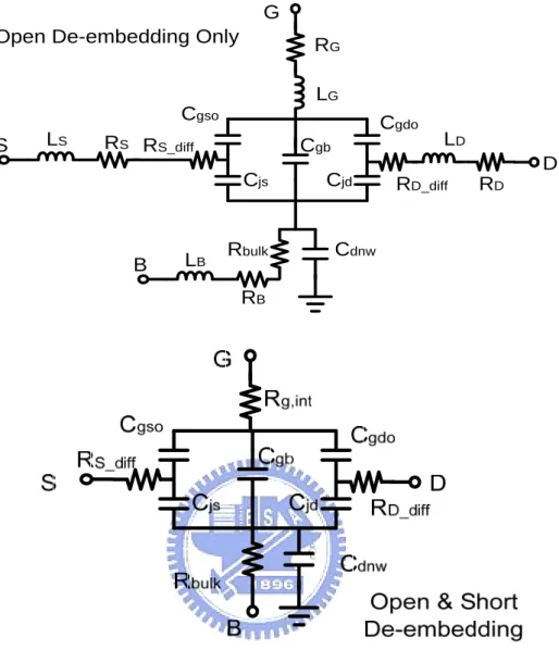
3.1 De-embedding methods and verification
The test structures of the RF MOSFET includes the actual device under test (DUT) and parasitic components form the metal interconnections to the pad structures, in order to model the behavior of the DUT accurately and extracting MOSFET parameters from measured data, to build de-embedding method is necessary for the purpose, and the de-embedding method in the thesis will use “open” and “short” de-embedding method.
3.1.1 Open de-embeddi
st structures is the full structure take off the layer under metal1(M1), and the open
a. Measure the S p
;
3
(3.2)
c. Subtract the Y parameter of the open pad from the Y parameters of DUT.
(3.3)
ng
The dummy open pad is designed to clear the parallel coupling capacitances, the te
de-embedding step can be describe as follows.
arameters of the DUT and transform it into Y parameters.
mea mea
S
→
Y
(3.1) b. Measure the S parameters of the dummy open pad and transform them into Y parameters. open open 1 3 3 C C C op Y +Y −Y ⎡ ⎤ S →Y 3 2 en C C C Y Y Y Y = ⎢ − + ⎥ ⎣ ⎦ _mea o mea open
Y
→
Y
−
Y
dummy open pad respectively, the open pad equivalent circuit is composed of
capacitance mainly, in Fig. 3.1, YC1 and YC2 are coupling parameters between pads
. ZRL1 ~
ZRL3 p
rameters of device, and the parameters can be used to calculate the s in equivalent circuit model.
T mbed
pa
ad structures uses the layout of open p
and reference ground, YC3 is the coupling parameter between two signal pads
arameters a
a
value of the component
he open de-e rallel with the DUT
re related to the metal line layout in each terminal of device, and the parameters will be discussed later in section 3.1.2. So far, we can get the first de-embed Y p
3.1.2 Short de-embedding
ding method can de-embed the parasitic components in , but there are still the parasitic components in series with the DUT. Thus, the dummy short pad is designed to clear the series parasitical
parameters, the dummy short p ad and
connected all terminals together in metal3, the short de-embedding step can be describe as follows.
a. Measure the S parameters of the Short pad and to execute open de-embedding. short
short
Y
S
→
;Y
short−
Y
open=
Y
short_o (3.4)b. Convert Ymea_o and Yshort_o parameters into Z parameters.
; (3.5) (3.7) o mea o mea_
→
Z
_Y
Y
short_o→
Z
short_o ⎥ ⎤ ⎢ = Z ⎦ ⎣ 3 2 + 3 _ RL RL RL o short Z Z Zc. Subtract the Z parameter of the Zshort_o from the Z parameters of Zmea_o.
o short o mea dut
Z
Z
Z
=
_−
_ (3.6) dut dut ⎡ZRL1+ZRL3 ZRL3Y
Z
→
Remember that all test structure have the parasitic capacitances between the g first in order to substrate the coupling param
arameters ZRL1~ZRL3
originate from metal interconnections between the terminal of DUT and the pad. The intrinsic Z parameters of the DUT can be obtained through conventional open and short de-embedding discussed above, the
parameters or S parameters for the need. Fig. 3.4 is a good illustration of showing
3.2 Parasitic re
g can be represented s Fig. 3.5. According to the layout, the metal line connects form metal3(M3) to
ance GSG pad and ground, so that, all test structure need to do the open de-embeddin
eters. The equivalent circuit of short pad is shown In Fig. 3.3, we support that there are only parasitic p
final Z matrix also can be converted to Y
de-embedding procedures discussed in preceding paragraphs.
sistance and inductance extraction and analysis
The two-port 3T RF MOSFET is implemented with common source configuration that source and body terminals are tied together in metal3 and grounding, and the terminals of DUT connect to GSG pad by metal line. In our experience, the parasitic resistance contributed from the metal line will affect the I-V characteristic of DUT. For the purpose, we will extract the parasitic RL parameters from short pad and extract RL parameters from device directly in this session.
3.2.1 Parasitic RL extraction from short pad
The equivalent circuit of short pad after open de-embeddin ametal8(M8), we assume that it is composed of parasitic resistance and induct only form metal interconnections between the DUT and the pad, and the parameters with subscript “ext” to represent extrinsic RL parameters.
de-embedding, the Z parameters can be express as follow:
(
)
(
)
(
)
⎤ ⎣ ⎡ + + + + + ext d ext s ext s ext s ext s ext s ext s ext g ext g o short R L j R L j R L j R L j R , , , , , , , , , _ ω ω ω ω(
⎥ ⎦ ⎢ + + + = ext s ext s ext d R j L L j Z , , , ω ω)
(3.8)addition, the parasitic resistance and inductance can be expressed by arrange the
In (3.8) in the form.
(
)
(
)
(
short o short o)
o short o short ext g ext sZ
Z
R
_ _ _ 12 _ 11 , 12 ,Re
; ext d o shortZ
Z
R
Z
R
12 22 , _Re
Re
−
=
−
=
=
(
)
(
)
(
short o short o)
ω
o short o short ext g ext sZ
Z
L
_ _ _ 12 _ 11 , 12 ,Im
−
=
(3.9)The extracted R and R have the weak frequency dependence at low frequency,
the behavior indicated that there are frequency term without considered at high frequency probably. Although it has the behavior, the p
ω
ω
ext d o shortZ
Z
L
Z
L
12 22 , _Im
Im
−
=
=
g,ext d,extarasitic RL parameters are
Table 3.1 The extracted extrinsic resistance and inductance of short pad Extracted extrinsic RL Rg_ext (Ω) Rd_ext (Ω) Rs_ext (Ω) Lg_ext (pH) Ld_ext (pH) Ls_ext (pH) extracted at low frequency.
AVG(2~5G) 0.355 0.589 0.228 57.05 57.72 15.11
3.2.2 Parasitic RL extraction from device
In chapter 3.2.1, we discuss the approximate parasitic resistance and inductance
When MOSFET operating in strong inversion region and Vds=0V, the equivalent
circuit the
from short pad, but this part of resistance and inductance come from metal connection between metal3 and metal8 only, in order to determine total terminal resistance come form metal1 to metal8, parasitic parameters are extracted from device after open de-embedding only directly.
pu our ory, p RL extraction method can be summarized as the following equation.
blishing in laborat arasitic
( )
( )
dut ch ch dutZ
R
R
Z
122
Re
122
Re
≈
⇒
=
⋅
(3.10)(
)
2
Re
12 _ ch S o meaR
R
Z
=
+
;R
S≈
R
s,ext (3.11) Re(
Z22)
=RD +RS +Rch o mea _ (3.12)(
)
4 ReZ11 =RG +RS + (3.13)(
)
_o ch mea R(
)
(
)
gd S G o mea S DL
L
Z
L
L
Z
_ 11 _ 221
Im
2
Im
ω
ω
−
+
=
−
+
=
, →0 ch gd o mea SC
R
C
2 2 122
4
ω
ch gd o meaC
R
L
Z
2 _Im
ω
=
−
ω (3.14)3.2.3 Frequency and bias dependence of Parasitic RL
It has been known that gate resistance will influenoise performance of RF MOSFET at high frequency, for the layout of multi-finger MOSFET, the gate/drain terminal is used p
resistance. The terminal parasitic RL represe
inductanc nsists of both intrinsic and e
The effective lumped resistance and inductance can be considered to have a gate bias dependent and a bias independent component, remember that the terminal of DUT connect to the GSG pad by metal only, it means that the bias independent parasitic RL contributed from the extrinsic metal interconnection between M3 and M8, and the bias dependent RL will be contributed from the intrinsic MOSFET device.
nce the input impedance and
arallel structure to reduce the gate/drain nts the effective lumped resistance and
We have extract the parameters from devices with various channel length (L) and cy, and observe that R
-1
ance and the gate electrode resist
gate finger number (NF) at several bias conditions under the suitable frequen
D and RG are almost const in short channel device but sensitive to the
gate bias at long channel device, the parasitic resistance decreases with gate bias
increases. Thus, the optimizing RG andRD verse (Vgs -Vth) at different geometry is
plotted in Fig. 3.7 and Fig. 3.8.
The effective gate resistance that consists of the distributed channel resist ance, the effective drain resistance that consists of the electrode resistance and the resistance contributed from the channel, the expression for gate/drain resistance model can be written as:
_ _ _ _
G g poly g ch
R
g bias g const gs thR
R
R
=
+
R
V
V
=
+
−
(3.15) _ _ _ D d poly d ch bias d _d const gs th
R
R
R
R
V
V
=
+
−
RG versus inverse of (Vgs -Vth) is plotted to obtain Rg_poly and Rg_ch, where Rg_poly
and Rg_ch represent the gate bias independent resistance and gate bias dependent
resistance respectively, Rg_poly
R
=
+
(3.16)can be determined from the linear regression of mea
uation in Fig. 3.8. It provides that electrode resistance is bias independent, but distributed channel resistance is bias independent again.
surement data intercept at (Vgs -Vth)-1=0, in addition, Rg_bias is obtained from the
slope of the liner regression equation in Fig. 3.7. Similarly, Rd_const can be determined
from the linear regression of measurement data intercept at (Vgs -Vth)-1=0, Rd_bias is
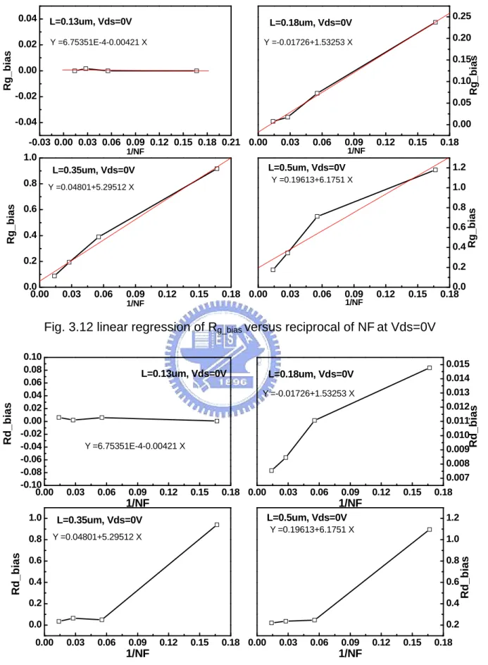
3.2.4 Device geometry dependence
In this session, we will discuss the geometry dfurther, the optimizing R t
1/L, and resistance of NQS effect is
The extracted R and R decrease with increasing finger number (NF) in
g_const, Rd_const, Rg_bias and Rd_bias
verse inverse of NF individually
G G
ependence of gate/drain resistance
G verse channel length at different Vgs is plotted in Fig. 3.9, i
shows that RG decreases first as channel length increase while showing a weak bias
dependence in the region, then to increase with channel length increase above 0.18um while showing a strong bias dependence. The channel length dependence of
RG is strong on longer device and at lower Vgs.
The U-shape channel length dependence of RG in Fig. 3.9 can be explained with
the consideration of the distributed effects in both distributed transmission line effect on the gate and NQS effect in the channel. It has been well known that the resistance of a poly-silicon resistor is proportional to
proportional to L.
g_const g_bias
the all devices, Fig. 3.10~3.13 show that extracted R
, the result support us that the linear regression of the resistances is a good reciprocal function of NF, and the behavior proved that the resistance originate from channel distributed effect obviously.
Using the method to separate the bias and geometry dependent and independent component from the R , the total parasitic resistance R can be written as below, where α, β almost is constant.
_ _ _ _ _
G g poly g ch g poly g nqs g bias gs th _ _
*
*
* (
)
g const g extR
R
R
R
R
R
R
V
V
L
R
L
NF
NF
V
gsV
thα
β
=
+
+
−
=
+
=
+
=
+
−
(3.17)The calculated Rg_poly and Rg_ch verse channel length show in the Fig. 3.14 and
Fig. 3.15. Rg_poly decrease with the channel length increasing, and Rg_ch increase with
the channel length increasing. When channel is short enough, the contribution of Rg_ch
is smaller than Rg_poly,, Rg_poly is gate bias insensitively and dominate the total
resis
-shape channel length dependence of the total gate terminal resistance.
3.3 Extraction of device parameters in linear region
In this section, we will discuss that parameters extraction of MOSFET operating in linear region. When gate voltage is smaller than the threshold voltage and at Vds=
ce extraction and analysis
Capacitances of RF MOSFET are extracted from the intrinsic Y parameters at low acitances extra
tance. As channel length increasing, the NQS effect is more significant, Rg_ch will
dominate the RG, and RG has a strong gate bias dependence. So that, it provides that
Rg_poly and Rg_ch cause the U
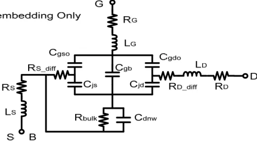
0V, the equivalent circuit of 3T device with parasitic RL parameters and substrate network components can be shown in Fig. 3.16. Cgs0 and Cgd0 represent the gate-to-source and gate-to-drain zero bias capacitances, respectively. Cgb is the total intrinsic and extrinsic gate-to-body capacitances. Cjs and Cjd are diffusion junction capacitances, Rsub represents the substrate resistance and Cdnw is junction capacitance between substrate and deep N-well.
3.3.1 Capacitan
frequency conventionally, short de-embedding is essential for accurate cap
ction in our experience. By performing Y parameter analysis on the circuit of intrinsic DUT in Fig. 3.17, the capacitance of equivalent circuit at low frequency can be express by
( )
( )
gg dutC
Y
11=
ω
Im
(3.18)( )
gd dut C Y =ω
−Im 12 (3.19)( )
(
gd jd)
dut C C Y22 =ω + Im (3.20)For Vgs>Vth,
C
gg=
C
gd+
C
gs. For Vgs<Vth,C
gg=
C
gdo+
C
gso+
C
gb.Note that the capacitances Cgs and Cgd are equal almost because the symmetry es includes both intrinsic and
pad in operating open de-embedding, and the capacitances decreases by a time constant decay with frequency
goodly dummy open/short pad. Thus, we still extract the capacitances of measured data at low frequency as the initial value of the circuit.
3.3
tance bias
etry dependence
structure in this bias condition. The extracted gate capacitanc
extrinsic component of the MOSFET individually, it also can be separated the bias dependent or independent part by the gate voltage. The extracted capacitances appear non-smooth curve in the smaller finger number devices with the frequency, because that small device has the small capacitances compared to the capacitances of the open
increasing, the issue can be solved by the
.2 Capaci
and geom
The gate-bias dependences of the optimizing capacitances are shown in Fig. 3.18, the intrinsic capacitance is normally bias dependent while the overlap capacitance is bias independent. when gate voltage small than the threshold voltage, To observe the transcapacitances conservation, the gate capacitances cab be rewrite as the equation Cgg=Cgd0+Cgs0+Cgb, As the gate voltage increases, the channel charges build up to increase the intrinsic component of the extracted capacitances, when the channel charge can be supplied by source/drain to channel rather than body in the strong inversion region, the whole Cgb capacitance which through the active
channel area to source/drain region is very small and can be neglected, the gate capacitances can describe as Cgg=Cgd+Cgs.
In the simplified C-V model, the gate capacitance can be described as equation ce geometry dependenc
(3.21). under a given gate voltage, we will discuss the capacitan
e, Fig. 3.19 and Fig. 3.20 show that the gate capacitances are well proportioned to the NF and channel length, the intercept of Y-axis is much closed to zero, and it verifies that the proposed extraction method is accurate and reliable.
* (
gs)
g active active ox
Q
=
W
L
C
V V
(3.21)3.3.3 Channel resistance extraction and analysis
When MOSFET operates at strong inversion region and Vds=0V, the extracted channel resistance Rch discussed above in question (3.10), Rch is considered as a intrinsic parameter originate form the inversion layer channel charge, the bias, NF, and channel length dependent are plotted in Fig. 3.21~Fig. 3.23, individually.
As the Vgs increasing, the channel charge can be supplied by source/drain to channel is increasing, the depths
finger number but is propositional to channel length.
nsic resistance from the device only.
FET is of inversion layer is increasing similarly, the behavior will cause the Rch decrease as vgs increase, Rch also decrease as NF increase base on the multi-finger gate/drain structure, but the total Rch is sum of the distributed channel resistance at the source/drain direction, Rch will increase with the longer channel length. So that, channel resistance is inverse proportion to gate voltage and
Rch is well propositional to geometry provided that the channel resistance is dominated by the intri
3.3.4 Substrate resistance extraction and analysis
One of the most important features to be considered when the MOSoper
T in Fig. 3.17, the parameters of equivalent circuit at low frequency can be express by:
ated at high frequencies is the impact of the substrate network on the output impedance. This substrate network consists of the junction capacitances and the substrate loss resistances, the drain junction capacitance and the bulk spreading resistance are represented by Cjd and Rsub, respectively.
As the operation frequency increases, the impedance of the junction capacitance reduces. The signal coupling through the substrate resistances from the drain to the source and from the drain/source to the substrate contact has to be carefully considered for the output admittance. By performing Y parameter analysis on the circuit of intrinsic DU
(
22 12)
Im
dut dut jdC
=
Y
+
Y
ω
(3.22)( )
2 2 22Re
dut sub jdR
=
Y
ω
C
(3.23)We will extract the substrate parameters using (3.23) as the initial value, In order to achieve the best fit for the simulated and measured S-parameter data, optimization of all the RF component values must be done. The optimizing Cjd and Rbulk geometry dependence are plotted in Fig. 3.24 and Fig. 3.25.
3.4 Extraction of intrinsic parameters in saturation region
y channel structure and current gain. The parameters gm and gds represent the transconductance and the output conductance
of the transistor respectively, and uniform channel resistance replace by Rch , Rds and
Cds parameters to express the asymmetry inversion
When MOSFET operating in saturation region, the equivalent circuit of DUT after open de-embedding can be represented as Fig. 3.26, the difference between linear region and saturation region is the asymmetr
layer.
summarized as the following equation, d m gs
I
g
V
∂
=
∂
; d ds dsI
g
V
∂
=
∂
(3.24)1
ch ds dsg
=
R
+
R
;R C
ch gs=
R C
ds gd (3.25) 1.2 0, 1.2 gs ds gs ds jd V V V jd V V VC
C
= ==
= = (3.26)3.4.1 Capacitance extraction and analysis
Extraction of capacitance at Vds=0V (3.18~3.20) to be suitable for use at this condition, the gate bias dependences of extracted capacitances are shown in Fig. 3.27 and Fig. 3.28, Cgs and Cgd are composed of the intrinsic and overlap components, the intrinsic capacitance is normally bias dependent while the overlap capa
acitances. Cgs has strong gate bias dependence in Fig. 3.27, Cg
bias increases near subthreshold region, and is saturation gradually in the strong inversion saturation region. Cgd only increases slightly with g
under saturation conditions, intrinsic capacitances of Cgd are very small because that drain voltage will deplete the drain side capacitance, an
citance is bias independent. As Vgs increases, the channel charges build up and increase the intrinsic component of the extracted cap
s increases strong as gate
ate bias in Fig. 3.28,
d the total gate-to-drain capacitance is dominated by the overlap capacitance.
From Fig. 3.27, it is observed that as Vds increases, there is a small increase in Cgs., this is because the transistor is approaching the saturation region and the channel is pinched-off when Vds=Vgs-Vth. The channel charge in the source side increases and the intrinsic capacitance of Cgs also increases. For Cgd, when the channel is approaching the pinch-off condition, the charge in the intrinsic drain region decreases and this decreases the intrinsic capacitance of Cgd.
The capacitance geometry dependence are plotted in Fig.3.29 ~ Fig. 3.32, the gate capacitances are well proportioned to the NF and channel length as the description in section 3.3.2.
Fig. 3.1 The equivalent circuit of 3T device with pad
Fig. 3.2 The equivalent circuit of open pad
Fig. 3.4 The illustration of de-embedding procedure for 3T device
R
g,extL
g,extL
d,extR
d,extR
s,extL
s,extPort1
Port2
Fig. 3.6 The equivalent circuit of 3T device at Vgs>>Vth, Vds=0V (Open_de) 0 2 4 6 8 10 12 14 2 4 6 8 10 12 14 Y =1.98+0 X Y =2.74222+0.00159 X Y =4.89+0 X 12.71+0 X L=0.13um, Vds=0 Y = NF=6 NF=18 NF=36 NF=72 R G 1/Vg-Vth 0 2 4 6 8 10 12 14 2 4 6 8 10 12 14 Y =1.93561+0.00755 X Y =2.37548+0.0173 X Y =3.95065+0.07304 X Y =10.0322+0.23748 X 0 L=0.18um, Vds= NF=6 NF=18 NF=36 NF=72 R G 1/Vg-Vth 0 2 4 6 8 10 12 14 5 10 15 20 Y =1.29187+0.08814 X Y =1.93053+0.1933 X Y =2.56023+0.39036 X Y =7.59692+0.91755 X L=0.35um, Vds=0 NF=6 NF=18 NF=36 NF=72 R G 1/Vg-Vth 0 2 4 6 8 10 12 14 2 4 6 8 10 12 14 16 18 20 22 24 L=0.5um, Vds=0 Y =1.28039+0.17593 X Y =1.38584+0.34572 X Y =2.74468+0.71231 X Y =6.65665+1.18009 X NF=6 NF=18 NF=36 NF=72 R G 1/Vg-Vth
0 2 4 6 8 10 12 14 0.6 0.8 1.0 1.2 1.4 1.6 1.8 2.0 Y =0.64563+0.00622 X Y =0.8002+0.00216 X Y =1.07174+0.00599 X Y =1.942+5.62066E-4 X L=0.13um, Vds=0 NF=6 NF=18 NF=36 NF=72 R D 1/Vg-Vth 0 2 4 6 8 10 12 14 0.4 0.8 1.2 1.6 2.0 2.4 Y =0.4824+0.00754 X Y =0.63818+0.00846 X Y =0.9714+0.01107 X Y =2.10659+0.01477 X L=0.18um, Vds=0 NF=6 NF=18 NF=36 NF=72 R D 1/Vg-Vth 0 2 4 6 8 10 12 14 0 5 10 15 20 Y =0.71329+0.03433 X Y =0.88487+0.06399 X Y =1.89061+0.04848 X Y =5.99764+0.94104 X L=0.35um, Vds=0 NF=6 NF=18 NF=36 NF=72 R D 1/Vg-Vth 0 2 4 6 8 10 12 140 5 10 15 20 25 Y =0.32146+0.22044 X Y =0.7015+0.23557 X Y =2.04675+0.24657 X Y =6.53914+1.09505 X L=0.5um, Vds=0 NF=6 NF=18 NF=36 NF=72 R D 1/Vg-Vth
Fig. 3.8 linear regression of optimized RD versus (Vgs -Vth)-1 at Vds=0V
0.1 0.2 0.3 0.4 0.5 8 10 12 14 16 18 20 22 0.1 0.2 0.3 0.4 0.5 3 4 5 6 7 8 9 10 11 12 0.1 0.2 0.3 0.4 0.5 2 3 4 5 6 0.1 0.2 0.3 0.4 0.5 1.4 1.6 1.8 2.0 2.2 2.4 2.6 2.8 3.0 3.2 3.4 3.6 R G ( Ω ) R G ( Ω ) NF=6, Vds=0V Vg=0.4V Vg=0.6V Vg=0.8V Vg=1.0V L (um) NF=18, Vds=0V Vg=0.4V Vg=0.6V Vg=0.8V Vg=1.0V L (um) R G ( Ω ) NF=36, Vds=0V Vg=0.4V Vg=0.6V Vg=0.8V Vg=1.0V L (um) R G ( Ω ) NF=72, Vds=0V Vg=0.4V Vg=0.6V Vg=0.8V Vg=1.0V L (um)
0.000 0.03 0.06 0.09 0.12 0.15 0.18 5 10 15 0.00 0.03 0.06 0.09 0.12 0.15 0.180 2 4 6 8 10 12 0.00 0.03 0.06 0.09 0.12 0.15 0.18 0 2 4 6 8 0.00 0.03 0.06 0.09 0.12 0.15 0.18 0 1 2 3 4 5 6 7 8 Y =0.90912+70.80926 X L=0.13um, Vds=0V Rg _po ly 1/NF Y =1.01627+53.91991 X L=0.18um, Vds=0V R g _ poly 1/NF Y =0.61219+41.42194 X L=0.35um, Vds=0V Rg _ poly 1/NF Y =0.49853+37.16637 X L=0.5um, Vds=0V R g _ pol y 1/NF
Fig. 3.10 linear regression of Rg_poly versus reciprocal of NFat Vds=0V
0.00 0.03 0.06 0.09 0.12 0.15 0.18 0.6 0.8 1.0 1.2 1.4 1.6 1.8 2.0 0.00 0.03 0.06 0.09 0.12 0.15 0.18 0.5 1.0 1.5 2.0 0.000 0.03 0.06 0.09 0.12 0.15 0.18 1 2 3 4 5 6 0.00 0.03 0.06 0.09 0.12 0.15 0.18 0 1 2 3 4 5 6 7 Y =0.56494+8.33579 X L=0.13um, Vds=0V Rd _po ly 1/NF Y =0.35191+10.57629 X L=0.18um, Vds=0V R d _ poly 1/NF Y =0.02319+35.59681 X L=0.35um, Vds=0V Rd _ poly 1/NF Y =-0.31365+41.16676 X L=0.5um, Vds=0V Rd _p ol y 1/NF
-0.03 0.00 0.03 0.06 0.09 0.12 0.15 0.18 0.21 -0.04 -0.02 0.00 0.02 0.04 0.00 0.03 0.06 0.09 0.12 0.15 0.18 0.00 0.05 0.10 0.15 0.20 0.25 0.00 0.03 0.06 0.09 0.12 0.15 0.18 0.0 0.2 0.4 0.6 0.8 1.0 0.00 0.03 0.06 0.09 0.12 0.15 0.180.0 0.2 0.4 0.6 0.8 1.0 1.2 Y =6.75351E-4-0.00421 X L=0.13um, Vds=0V Rg_bias 1/NF 1/NF Y =-0.01726+1.53253 X L=0.18um, Vds=0V Rg_bias Y =0.04801+5.29512 X L=0.35um, Vds=0V Rg _ b ias 1/NF 1/NF Y =0.19613+6.1751 X L=0.5um, Vds=0V Rg _ b ia s
Fig. 3.12 linear regression of Rg_bias versus reciprocal of NFat Vds=0V
0.00 0.03 0.06 0.09 0.12 0.15 0.18 -0.10 -0.08 -0.06 -0.04 -0.02 0.00 0.02 0.04 0.06 0.08 0.10 0.00 0.03 0.06 0.09 0.12 0.15 0.18 0.007 0.008 0.009 0.010 0.011 0.012 0.013 0.014 0.015 0.00 0.03 0.06 0.09 0.12 0.15 0.18 0.0 0.2 0.4 0.6 0.8 1.0 0.00 0.03 0.06 0.09 0.12 0.15 0.18 0.2 0.4 0.6 0.8 1.0 1.2 Y =6.75351E-4-0.00421 X L=0.13um, Vds=0V Rd _ b ia s 1/NF Y =-0.01726+1.53253 X L=0.18um, Vds=0V Rd _ b ia s 1/NF Y =0.04801+5.29512 X L=0.35um, Vds=0V Rd _ b ia s 1/NF Y =0.19613+6.1751 X L=0.5um, Vds=0V Rd _ b ia s 1/NF
2 3 4 5 6 7 8 6 8 10 12 14 2 3 4 5 6 7 8 2.0 2.5 3.0 3.5 4.0 4.5 5.0 5.5 6.0 2 3 4 5 6 7 8 1.0 1.5 2.0 2.5 3.0 2 3 4 5 6 7 8 1.0 1.2 1.4 1.6 1.8 2.0 2.2 2.4 NF=6, Vds=0V Rg _ p o ly 1/L NF=18, Vds=0V Rg _p o ly 1/L NF=36, Vds=0V R g _ poly 1/L NF=72, Vds=0V Rg _p o ly 1/L
Fig. 3.14 channel length dependence of Rg_polyat Vds=0V
0.1 0.2 0.3 0.4 0.5 0 2 4 6 8 10 12 14 16 R g_c h L (um) NF=36, Vds=0V Vg=0.4V Vg=0.6V Vg=0.8V Vg=1.0V NF=6, Vds=0V Vg=0.4V Vg=0.6V Vg=0.8V Vg=1.0V NF=18, Vds=0V Vg=0.4V Vg=0.6V Vg=0.8V Vg=1.0V NF=72, Vds=0V Vg=0.4V Vg=0.6V Vg=0.8V Vg=1.0V 0.1 0.2 0.3 0.4 0.5 0 1 2 3 4 5 6 7 8 9 R g_ ch L (um) 0.1 0.2 0.3 0.4 0.5 0 1 2 3 4 5 R g_ c h L (um) 0.1 0.2 0.3 0.4 0.5 0.0 0.5 1.0 1.5 2.0 2.5 R g_ ch L (um)
Fig. 3.16 The equivalent circuit of 3T device at Vgs=Vds=0V (Open_de)
0.4 0.6 0.8 1 20 40 60 80 100 120 140 160 180 200 220 L=0.13um, Vds=0 NF=6 NF=18 NF=36 NF=72 Cg d (fF ) Vg (V) 0.4 0.6 0.8 1 50 100 150 200 250 300 L=0.18um, Vds=0 NF=6 NF=18 NF=36 NF=72 Cg d (fF ) Vg (V) 0.4 0.6 0.8 1 100 200 300 400 500 600 700 L=0.35um, Vds=0 NF=6 NF=18 NF=36 NF=72 Cg d (fF ) Vg (V) 0.4 0.6 0.8 1 100 200 300 400 500 600 700 800 900 L=0.5um, Vds=0 NF=6 NF=18 NF=36 NF=72 C Vg (V)
Fig. 3.18 The bias dependence of optimized Cgd at Vds=0V
) g d (fF 0 10 20 30 40 50 60 70 80 0 50 100 150 200 250 0 10 20 30 40 50 60 70 800 50 100 150 200 250 300 350 0 10 20 30 40 50 60 70 80 0 100 200 300 400 500 600 700 0 10 20 30 40 50 60 70 800 100 200 300 400 500 600 700 800 900 1000 L=0.13um, Vds=0V Vg=0.4V Vg=0.6V Vg=0.8V Vg=1.0V C g d (fF ) NF L=0.18um, Vds=0V Vg=0.4V Vg=0.6V Vg=0.8V Vg=1.0V C gd ( fF) NF L=0.35um, Vds=0V Vg=0.4V Vg=0.6V Vg=0.8V Vg=1.0V C g d (fF ) NF L=0.5um, Vds=0V Vg=0.4V Vg=0.6V Vg=0.8V Vg=1.0V C g d (fF ) NF
0.1 0.2 0.3 0.4 0.5 20 30 40 50 60 70 80 90 0.1 0.2 0.3 0.4 0.5 40 60 80 100 120 140 160 180 200 220 240 260 0.1 0.2 0.3 0.4 0.5 100 150 200 250 300 350 400 450 500 0.1 0.2 0.3 0.4 0.5 C gd ( fF) NF=6, Vds=0V 200 300 400 500 0 0 80 900 1000 60 70 0 Vg=0.4V Vg=0.6V Vg=0.8V Vg=1.0V L (um) C NF=18, Vds=0V Vg=0.4V Vg=0.6V Vg=0.8V g d (fF ) Vg=1.0V L (um) C gd ( fF) NF=36, Vds=0V L C gd ( fF) NF=72, Vds=0V Vg=0.4V Vg=0.4V Vg=0.6V Vg=0.6V Vg=0.8V Vg=0.8V Vg=1.0V L Vg=1.0V (um) (um)
Fig. 3.20 The channel length dependence of optimized Cgd at Vds=0V
0 2 4 6 8 10 12 14 0 50 100 150 200 250 300 350 400 450 NF=6, Vds=0 L=0.13um L=0.18um L=0.35um L=0.5um Rch 1/(Vg-Vth) 0 2 4 6 8 10 12 140 20 40 60 80 100 120 140 NF=18, Vds=0 L=0.13um L=0.18um L=0.35um L=0.5um Rc h 1/(Vg-Vth) 0 2 4 6 8 10 12 14 0 10 20 30 40 50 60 70 NF=36, Vds=0 L=0.13um L=0.18um L=0.35um L=0.5um Rc h 1/(Vg-Vth) 0 2 4 6 8 10 12 140 5 10 15 20 25 30 35 40 NF=72, Vds=0 L=0.13um L=0.18um L=0.35um L=0.5um Rc h 1/(Vg-Vth) Fig. 3.21 The bias dependence of optimized Rch at Vds=0V