國
立
交
通
大
學
電子工程學系電子研究所碩士班
碩 士 論 文
使用不易受偏移影響斜率偵測器之具有大輸入動
態範圍可適性電纜等化器
Adaptive Equalizers with large Input Dynamic
Range Using Offset-Insensitive Slope Detector
研 究 生:魏暐庭 Wey-Tin Wei
指導教授:蔡嘉明 教授 Prof. Chia-Ming Tsai
使用不易受偏移影響斜率偵測器之具有大輸入動
態範圍可適性電纜等化器
Adaptive Equalizers with large Input Dynamic
Range Using Offset-Insensitive Slope Detector
研 究 生:魏暐庭 Student:Wey-Tin Wei
指導教授:蔡嘉明 教授 Advisor:Prof. Chia-Ming Tsai
國 立 交 通 大 學
電子工程學系電子研究所碩士班
碩 士 論 文
A Thesis
Submitted to Department of Electronics Engineering & Institute of Electronics College of Electrical and Computer Engineering
National Chiao Tung University in partial Fulfillment of the Requirements
for the Degree of Master
in
Electronics Engineering Tune 2012
Hsinchu, Taiwan, Republic of China 中華民國一 0 一年六月
I
使用不易受偏移影響斜率偵測器之具有大輸入動
態範圍可適性電纜等化器
學生:魏暐庭
指導教授:蔡嘉明 教授
國立交通大學
電子工程學系電子研究所碩士班
摘 要
本論文提出使用斜率偵測器之可適性等化器。此偵測機制可避免使用整流器 而造成電路容易受偏移(offset)影響。而斜率偵測器會偵測訊號的斜率資訊用以 判斷可適性等化器需要提供多少的增益補償。並且,使用了振幅偵測器及共模準 位偵測器,增加可適性等化器所能承受的輸入動態範圍。為了使等化器可以減少 功率消耗,提出了使用正迴授概念的等化器。而此可適性等化器使用了 65nm CMOS 製程做驗證,在 1.2 伏特的電壓供應器及 13.5Gb/s 的速度下,可補償 20.5dB 的 通道損耗,並且只消耗了 14mW 的功率。並且在附錄 A 裡,描述一個使用了 0.18μm CMOS 製程做驗證的可適性等化器,在 1.8 伏特的電壓供應器及 6Gb/s 的速度下, 可補償 23.3dB 的通道損耗,並且消耗了 27mW 的功率。II
Adaptive Equalizers with large Input Dynamic
Range Using Offset-Insensitive Slope Detector
Student:Wey-Tin Wei
Advisor:Prof. Chia-Ming Tsai
Department of Electronics Engineering & Institute of Electronics
National Chiao Tung University
Abstract
The thesis presents adaptive equalizers using the slope detector. The detection mechanism avoids using the rectifiers for decreasing the sensitive of offset. The edge-speed is detected by slope detector to adjust the gain-boost of equalizer. Furthermore, with the help of swing detector and common-mode detector, it extends the input dynamic range of adaptive equalizer. In this work, we proposed the positive-feedback based adaptive equalizer to provide more gain-boost without scarifying the power consumption. This chip can work at 13.5Gb/s data rate, and compensates 20.5dB channel loss at Nyquist rate while consuming only 14mW (without output buffer) from a 1.2V power supply in 65nm CMOS technology. Furthermore, in the appendix A, we proposed a 6Gb/s adaptive equalizer using slope detector. It can compensate 23.3dB channel loss from a 1.2V power supply with 27mW power consumption in 0.18μm CMOS technology
III
誌 謝
碩士班的生涯即將告一段落,誠摯的感謝求學期間所有協助過我的人。 碩士學位能夠順利完成,首要感謝我的指導教授 蔡嘉明博士的費心指導。 在研究上,教授總是不厭其煩的引導我,培養我獨立思考及問題解決的能力。在 研究過程中,每當我遇到低潮、受到打擊時,教授總是不斷的激勵我,給我勇氣 和信心,讓我能再接再厲,愈挫愈勇。感謝教授這三年來的諄諄教誨,這份恩情, 我將永遠銘記在心。另外,特別感謝 陳巍仁教授、洪浩喬教授、黃弘一教授能夠 擔任我的口試委員,並給予許多寶貴的建議與指導,使此份論文能更加完善。 感謝實驗室的博瑋學長,不僅在研究上提供我許多協助,在平常的相處也 不時與我分享生活上的經驗,讓我在待人處事方面也能有所成長,對於迎接未來 的挑戰也能更有信心。感謝勖哲學長、致煌學長、至中學長在研究上給予我許多 的指導,讓我在研究的過程能更順利。感謝振鵬學長、光仁、柏均、瑜聰、勝凱、 安修與易弘在研究和實驗室事務上提供許多協助和幫忙,並時常與我討論研究相 關事宜,促進彼此的進步和成長。感謝電資303實驗室的盈杰學長和馨庭提供我在 晶片量測上的協助,還有感謝世豪學長、柏硯學長及子超學長的用心指導,讓我 能順利使用鼎勳實驗室裡的儀器,讓晶片的量測能夠如期完成。 另外,感謝我所有的好友。感謝交大電子所的同學們這三年來的打氣與鼓 勵,同學們彼此間的支援與協助,是讓我能順利完成此份論文最大的關鍵。感謝 中正大學及羅東高中的好友們,很開心一路走來始終有他們的陪伴,在重要時刻 總能及時拉我一把,給我最大的鼓舞,讓我能重燃信心,繼續努力。 最後,感謝我的家人,在生活與精神上給予我最大的支持,讓我能無憂無 慮的完成學業。特別感謝真如無怨無悔的陪伴,多年來的包容與支持,是讓我持 續堅持下去的最大動力。 謹以此論文獻給摯愛的諸位。感謝你們。 魏暐庭 2012/8/4IV
Table of Contents
摘 要 ... I Abstract ... II List of Figures ... VI List of Tables ... X Chapter1 Introduction ... 1 1.1 Motivation ... 1 1.2 Wireline Communication ... 2 1.3 Thesis Organization ... 4Chapter2 The Basic Concepts of Adaptive Equalizer ... 5
2.1 Basic Concepts ... 5
2.1.1 Pseudo-Random Binary Sequence (PRBS) ... 5
2.1.2 Bandwidth Requirement ... 6
2.1.3 Eye-diagram... 7
2.1.4 Jitter ... 8
2.1.5 Noise, SNR and BER ... 9
2.1.6 Channel Characteristic and Modeling ... 10
2.1.7 Priciple of Adaptive Equalizer Operation ... 11
2.2 High-frequency Boosting Technique review ... 12
2.2.1 Capacitive Degeneration Technique ... 12
2.2.2 Inductive Peaking Technique ... 14
2.3 Adaptive Equalizer Review ... 14
2.3.1 Adaptive Equalizer with slope detectors ... 14
2.3.2 Adaptive Equalizer Using Enhanced Low-Frequency Gain Control Method ... 16
V
2.3.3 Adaptive Equalizer Using Direct Measurement of The Equalizer Output
Amplitude ... 17
2.3.4 Adaptive Equalizer with Spectrum-Balancing Technique ... 18
Chapter3 The Design Concept of Slope Detector ... 20
3.1 Motivation ... 20
3.2 The operation Procedure of Slope Detector ... 21
Chapter4 A 13.5Gb/s Positive-Feedback based Adapative Equalizer with Large Input Dynamic Range Using Offset-Insensitive Slope Detector... 29
4.1 Motivation ... 29 4.2 Architecture ... 30 4.3 Circuits Design ... 32 4.3.1 Equalizer ... 32 4.3.2 Common-Mode Detector ... 43 4.3.3 Swing Detector ... 43
4.3.4 Slope Detector, Current Mirror and Integrator ... 47
4.4 Layout and Simulation Results of Complete Chip ... 51
4.4.1 Layout Design ... 51
4.4.2 Simulation Results of Complete chip ... 53
4.5 Experimental Results ... 55
4.5.1 Die Photo ... 55
4.5.2 Chip Measurement ... 55
Chapter5 Conclusion and Future Work ... 69
Appendix A A 6Gb/s Adaptive Equalizer with Large Input Dynamic Range Using Offset-Insensitive Slope detector ... 70
VI
List of Figures
Fig. 1.1. Typical Serial Link Transceiver ... 2
Fig. 2.1. The example of 23-1 PRBS. ... 6
Fig. 2.2. Comparison between sufficient bandwidth and insufficient bandwidth. ... 7
Fig. 2.3. Eye-opening. ... 8
Fig. 2.4. Jitter classifications. ... 9
Fig. 2.5 Channel model with skin effect and dielectric loss consideration ... 11
Fig. 2.6 Diagram of equalizer operation ... 11
Fig. 2.7. Equalizing filter with RC degeneration technique. ... 12
Fig. 2.8. Magnitude response of RC degeneration technique. ... 13
Fig. 2.9. Equalizing filter with inductive peaking technique... 13
Fig. 2.10. Magnitude response of inductive peaking technique. ... 13
Fig. 2.11. Architecture of adaptive equalizer with slope detectors. ... 15
Fig. 2.12. Slope detector. ... 15
Fig. 2.13. The transient response comparison of slope detector. (a) comparison between sharp and blunt slope (b) comparison between w/o and w/ offset ... 15
Fig. 2.14. Architecture of adaptive equalizer using enhanced low-frequency gain-control. ... 17
Fig. 2.15. Architecture of adaptive equalizer using direct measurement of the equalizer output amplitude. ... 18
Fig. 2.16. The relation between high-frequency and low-frequency components. ... 18
Fig. 2.17. Architecture of adaptive equalizer with spectrum-balancing technique. ... 19
Fig. 2.18 Spectrum decomposition. ... 19
VII
Fig. 3.2. The comparison between sharp slope and blunt slope. ... 22
Fig. 3.3. The comparison between large swing and small swing. ... 22
Fig. 3.4. The basic architecture of adaptive equalizer using slope detector. ... 23
Fig. 3.5. The comparison between different swings when Vos_built-in is fixed. ... 23
Fig. 3.6. The linear model of adaptive equalizer using slope detector with offset consideration. ... 24
Fig. 3.7. The linear model for offset sensitivity analysis. (a) the offset effect at low-frequency path (b) the offset effect at high-frequency path. ... 25
Fig. 3.8. The linear model of adaptive equalizer using duo-loop control with offset consideration. ... 26
Fig. 3.9. The linear model for offset sensitivity analysis. (a) the offset effect at low-frequency path (b) the offset effect at high-frequency path ... 27
Fig. 4.1. (a) The magnitude response of 18-inch channel (b) The Transient response of 18-inch channel ... 30
Fig. 4.2. Cascading four differential pairs to compensate 18-inch channel. (a) Without reverse scaling technique (b) With reverse scaling technique ... 32
Fig. 4.3. The block diagram of positive feedback system. ... 32
Fig. 4.4. The improved positive feedback system. ... 32
Fig. 4.5. (a)The basic implemented schematic and magnitude response of positive-feedback based equalizer. (b) the half-circuit of (a) ... 33
Fig. 4.6. Block diagram of Equalizer. ... 35
Fig. 4.7. The schematic and magnitude response of gm-boosted technique. ... 35
Fig. 4.8. The schematic and magnitude response of the first stage. ... 36
Fig. 4.9. The schematic and magnitude response of the second stage. ... 36 Fig. 4.10. The magnitude response of the first three stage. (a) the first stage (b) the
VIII
second stage (c) the third stage ... 37
Fig. 4.11. The normalized delay response of equalizer ... 39
Fig. 4.12. (a) Magnitude response of the fourth stage. (b) Group delay response the fourth stage. ... 40
Fig. 4.13. (a) Magnitude response comparison. (b) Group delay response comparison. 41 Fig. 4.14. Eye-diagrams comparison (a) without the fourth stage (b) with the fourth. .. 42
Fig. 4.15. The schematic and magnitude response of the fifth stage ... 42
Fig. 4.16. The magnitude response of equalizer under different Vctrl. ... 43
Fig. 4.17. The schematic of common-mode detector ... 44
Fig. 4.18.The schematic of swing detector. ... 44
Fig. 4.19. The relation of VEQ and VSW. ... 44
Fig. 4.20. (a) Magnitude response of swing detector. (b) Phase response comparison of swing detector. ... 45
Fig. 4.21. The relations between input swingp-p, expected VSW and simulated VSW. ... 46
Fig. 4.22. The schematic of slope detector, current mirror, and integrator. ... 47
Fig. 4.23. The relations between input swingp-p and simulated Vos_built-in... 49
Fig. 4.24. The relationship between VEQ+, VEQ-, IA, IB, IC, ID, I1 and I2. ... 48
Fig. 4.25. The simulated transient responseof VEQ+ , VEQ- and I1-I2. ... 49
Fig. 4.26. The simulated (I1-I2)avg when input signal is attenuated with different channel loss. ... 50
Fig. 4.27. (a) The overall layout view of chip. (b) The zoom-in view of active schematics. ... 52
Fig. 4.28. The magnitude response of (a) channels (b) equalizer under different Vctrl. 53 Fig. 4.29. Simulated eye-diagrams which is before equalization with (a) 18-inch (b) 4-inch ... 54
IX
Fig. 4.30. Simulated eye-diagrams which is after equalization with (a) 18-inch (b)
4-inch ... 54
Fig. 4.31. Die photograph of chip. ... 55
Fig. 4.32. S21 testing setup of channel ... 56
Fig. 4.33. Time-domain testing setup of chip, including channels and cables. ... 56
Fig. 4.34. PCB layout view. ... 57
Fig. 4.35. Test kit of PCB trace, about 2-inch of length. ... 57
Fig. 4.36. Measured S21 of channels. ... 58
Fig. 4.37. Measured S21 of cable. ... 58
Fig. 4.38. Measured S21 of overall chip. ... 59
Fig. 4.39. Measured eye-diagrams which is before equalization with 400mV input swing and (a) 20-inch (b) 14-inch (c) 2-inch ... 60
Fig. 4.40. Measured eye-diagrams which is after equalization with 300mV input swing and (a) 20-inch (b) 14-inch (c) 2-inch ... 61
Fig. 4.41. Measured eye-diagrams which is after equalization with 400mV input swing and (a) 20-inch (b) 14-inch (c) 2-inch ... 62
Fig. 4.42. Measured eye-diagrams which is after equalization with 500mV input swing and (a) 20-inch (b) 14-inch (c) 2-inch ... 63
Fig. 4.43. Measured eye-diagrams which is after equalization with 600mV input swing and (a) 20-inch (b) 14-inch (c) 2-inch ... 64
Fig. 4.44. The jitter comparison. ... 65
Fig. 4.45. The Vctrl comparison. ... 65
Fig. 4.46. The measured results of chip. (a) utilizing Spectrum analyzer (Agilent E4440A) (b) utilizing oscilloscope (Agilent 86100A) ... 66
X
List of Tables
1
Chapter 1
Introduction
1.1 Motivation
With the rapidly-growing data communication of microprocessors and memories in recently years, the high speed data communication is an important issue in the modern technique. The conventional parallel communication becomes an inefficient way, because of it demands numerous transmission lines, pins and area which would increase the cost. Hence, the serial-link communication is a potential way for the high speed data communication. In the serial-link communication, the requirement of high bandwidth at I/O interface becomes the bottleneck, especially at tens Gb/s data rate. Consequently, the high speed adaptive equalizer plays a critical role in the serial-link communication for overcoming the inter-symbol interface (ISI) effect which resulted from the insufficient bandwidth. Furthermore, the insufficient bandwidth is caused by frequency-dependent loss of channel.
2
1.2 Wireline Communication
P2S FIR Filter+ Output Driver Channel EQ S2P PLL CLKref CDR Transmitter ReceiverFig. 1.1. Typical Serial Link Transceiver
For the high-speed application, the conventional parallel data communication is no longer useful. Because of numerous data pins increase loading which restricts the speed of data transferring. So, in the modern world, the high-speed serial link transceiver system is the popular system for high-data-rate wireline communication. Fig. 1.1 shows a typical serial link transceiver system. A typical serial link transceiver system consists three main parts: transmitter, channel and receiver.In the transmitter, a parallel-to-serial interface (P2S) would serialize parallel data to form serial data. A Phase-Locked Loop is an oscillator-generated signal which is phase and frequency locked to be a reference signal for the serial data. The finite impulse response (FIR) filter pre-distorts transmitted pulse in order to cancel the channel impulse response. And the output driver is designed for driving output loading, so it must provide sufficient driving current to produce enough output swing for the receiver.
The channel is responsible for delivering the serial data from the transmitter to the receiver. But the channel loss would degrade the high-frequency power of the
3
high-speed transferred data. The channel loss which caused by skin effect and dielectric loss will results in the high-speed transferred data suffers serious inter-symbol interface (ISI). The ISI will increase bit-error-rate (BER).
In the receiver, because of channel loss, we usually utilize equalizer (EQ) to compensate the high-frequency part of signal. In order to perform synchronous operation such as retiming and demultiplexing in random data, the receiver side demands a clock-and-data recovery (CDR). It can not only retime the data for less jitter, but also regenerate the noiseless data. And, at last, the serial data is deserialized to the parallel data by the serial-to-parallel interface (S2P).
As the mention before, for the high-speed serial data communication, we need to do equalization which can solve the effect of ISI. There are three ways to do equalization: pre-emphasis [1-2], linear equalizer (LEQ) [3-9] and decision feedback equalizer (DFE) [10-13]. The pre-emphasis is applied in the transmitter side. It pre-amplifies the high-frequency part of signal to resist the distortion which caused by channel. In the receiver side, LEQ and DFE are popular techniques to do equalization. The DFE can reduce the post-cursor and be more tolerable to noise. It also can retime the serial data to get smaller jitter and better signal-to-noise ratio. And there are some adaptive algorithms to be applied with DFE, such as least-mean-square (LMS). But DFE requires large digital schematicry and enormous power consumption for high-speed application. And it can’t equalize large channel loss which has resulted in small eye-opening. The LEQ, in contrast with DFE, is less power consumption and can compensate more channel loss. And there are also many the adaptive algorithms is popular and usable for LEQ to compensate different channel loss and robust to environment variation, like PVT variation. These different adaptive algorithms which had been published will be introduced in the later chapter.
4
1.3 Thesis Organization
This thesis is composed of six chapters.
Chapter 1 describes the background on the research topic and introduces wireline communication systems.
Chapter 2 describes the basic concepts of equalizer, and provides definition to commonly-used expressions, such as eye opening and jitter. In addition, this chapter will review the correlative research in recent years about the adaptive equalizers.
Chapter 3 introduces the design concept of slope detector.
Chapter 4 describes: “A 13.5Gb/s Positive-Feedback based Adaptive Equalizer with Large Dynamic Range Using Offset-Insensitive Slope-Detection”. The adaptive equalizer’s architecture and the design concept of positive-feedback based equalizer would be introduced with simulated results. Layout considerations are described and measured results are given. The chapter concludes with a comparison with recent related published works.
Chapter 5 gives a conclusion to this thesis, as well as a description of the potential possibilities of future research topics related to the works in this thesis.
5
Chapter 2
The Basic Concepts of Adaptive
Equalizer
In this chapter, we introduce the necessarily basic concepts for analyzing and designing the adaptive equalizer. And then, we review the development of recently adaptive equalizer design, including linear equalizer (LEQ) schematics and adaptive algorithms.
2.1 Basic Concepts
2.1.1 Pseudo-Random Binary Sequence (PRBS)
A random binary data are composed with logical ZEROs and ONEs. If the time of one-bit is Tb seconds means the data rate is 1/Tb bits per second. The real random binary
data may occur with the long string of consecutive logical ZEROs or ONEs. We call this string as “a low transition density”, also mean low speed. Such low transition density would make the trouble for the schematic design, like offset cancellation. So, we usually will specify the longest string of consecutive logical
6 7 bits (7 Tb)
(the longest consecutive string) 3 bits
Fig. 2.1. The example of 23-1 PRBS.
ZEROs or ONEs. For the above reason, the pseudo-random binary sequence (PRBS) is the commonly used data pattern [14]. It can be generated by linear feedback shift register (LFSR) [15] which would generate a maximum sequence, 2m-1 bits, and repeat the sequence again and again. Each sequence contains 2m-1-1 ZEROs and 2m-1 ONEs, and the longest consecutive logical ZEROs or ONEs would equal to m bits. An example is depicted in Fig. 2.1.
2.1.2 Bandwidth requirement
In high-speed schematics design, how to design bandwidth is an important issue. The bandwidth trades with many other specifications, such as noise, power consumption and gain boost. For example, if we design a large bandwidth, the signal information can be preserved without distortion. But, in the meanwhile, the noise is also preserved which destroys the signal information. On the contrary, if we design a small bandwidth, although the noise could be decreased. But the signal is also distorted which is known as inter-symbol interface (ISI) [14] which due to insufficient bandwidth, insufficient
7
t
1Fig. 2.2. Comparison between sufficient bandwidth and insufficient bandwidth.
phase linearity, and insufficient low-frequency cutoff, as depicted in Fig. 2.2. At t1, the
signal have the error bit. This undesired phenomenon would corrupt the voltage level of ZEROs and ONEs, and result in the error bits. The rule of thumb for optimum bandwidth is 0.7 of data rate, Eq. (2.1) [14-15]. However, for modern high-speed data communication, this rule of thumb is no longer suitable. Because of the trade-off between bandwidth, power consumption and other specifications in high-speed application, the recently published paper usually setting bandwidth to be 0.5 of data rate[4, 9, 16], especially when the data rate is more than 10Gb/s. Furthermore, we call the 0.5 of data rate to be “Nyquist rate”. And we always pay attention to how much gain boost can be provided by equalizer at the Nyquist rate in adaptive equalizer design.
2.1.3 Eye-diagram
An eye-diagram is formed by folding all of signal into a particular time. The eye-diagram could provide us a lot of useful signal information, such as ISI, noise,
Insufficient bandwidth Sufficient bandwidth
8 Vertical eye-opening Horizontal eye-opening Jitterp-p Jitterp-p Fig. 2.3. Eye-opening.
signal slope and signal swing. And the eye-opening and jitter are the important specifications which can help us to judge the signal quality.
The eye-opening includes horizontal eye-opening and vertical eye-opening, as shown in Fig. 2.3. The horizontal eye-opening means the time interval which we successfully sample the signal’s logical level. The vertical eye-opening means the tolerant noise for the signal, this can be explained by signal-to-noise ratio (SNR).
2.1.4 Jitter
Jitter is defined as the deviation of a timing event from its ideal position. We usually measure it from eye-diagram, and the peak-to-peak measurement is often used to represent the amount of jitter (jitterp-p) which is shown in Fig. 2.3.
The jitter is composed with random jitter and deterministic jitter. The random jitter, as its name describing, is an unpredictable jitter. It’s resulted from noise, such as thermal noise and flicker noise, which occurring from semiconductors and components. So, the random jitter can be well approximation by Gaussuan distribution, or called normal distribution. Because of that, we usually specify the random jitter by root-mean-square value which means the standard
9 Jitter Random Jitter Deterministic Jitter Data-Dependent Jitter Periodic Jitter Duty-Cycle- Dependent Jitter
Fig. 2.4. Jitter classifications.
deviation of gaussian distribution. The deterministic jitter is a predictable jitter, and the peak-to-peak value is bounded. Furthermore, it can be divided into data-dependent jitter (DDJ), periodic jitter (PJ) and duty-cycle distortion jitter (DCDJ), as shown in Fig. 2.4. The value of DDJ is affected by the surrouding bits, in other word that is the ISI effect. The PJ is generated with the crosstalk. The DCDJ happens when the rising edges and falling edges of signal don’t cross each other at decision threshold voltage.
2.1.5 Noise, SNR and BER
For the high-speed data communication, bit-error-rate (BER) which is defined as the ratio of number of error bits occurring to the number of transferred bits is a key issue. The BER is defined as
the number of error bits
BER (2.1)
the number of transferred bits
For fitting in with a given BER. It can be designed by signal-to-noise ratio (SNR) [14], which is derived as p p noise,rms V SNR BER Q( ) Q( ) (2.2) 2V 2
10
And the Q function is defined as:
2 u ( ) 2 x 1 Q(x) e du (2.3) 2
By the (2.2), for example, if we want the BER to be smaller than 10-12, the SNR need to be larger than 14. That is to say when our signal swing is only 100mVp-p, the value of
noise has only 7mV of tolerant range. In high-speed and low-power design, noise would be a serious limitation in the modern data communication. Thus, the BER can help us to know how much noise can be tolerated on the trade-off between noise and bandwidth, and power consumption.
2.1.6 Channel Characteristic and Modeling
As the description in chapter 1, we need a channel to transferred serial data from transmitter to receiver. The channel loss would degrade the high-frequency power of signal. The cause of channel loss are skin effect and dielectric loss. The skin effect causes the current tend to flow at the surface of conductor. This phenomenon results in more and more effective resistance for signal, especially at high frequency. The dielectric loss is resulted from the heating effect on the dielectric material.
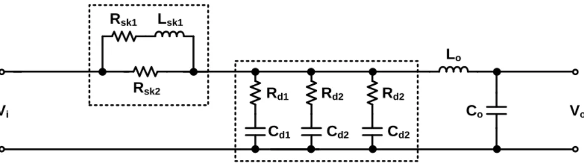
When we model the channel loss, we also bring these two effects into the channel model. The channel model is shown in Fig. 2.5 [16].
11 Rd1 Rd2 Rsk2 Rsk1 Lsk1 Cd1 Cd2 Lo Co Rd2 Cd2 Vi Vo
Fig. 2.5 Channel model with skin effect and dielectric loss consideration
Channel
Equalizer
Nyquist rate Nyquist rate Nyquist rateFreq. Freq. Freq.
Gain Gain Gain
Detection
circuit
Fig. 2.6 Diagram of equalizer operation
2.1.7 Priciple of Adaptive Equalizer Operation
In the receiver equalization, the linear equalizer (LEQ) is usually called equalizer (EQ) for short. As Fig. 2.6 showing, the channel degrades the high-frequency gain of signal. Thus, we use EQ to compensate the channel loss from moderate-frequency to Nyquist rate. Because of the various channel loss when the channel length is changing, there is in want of a detection schematic to judge whether the channel loss is compensated well or not. If not, the detection schematic would adjust the gain-boost of EQ until the channel loss is compensated well.
12
2.2 High-frequency boosting technique review
2.2.1 RC degeneration technique
Vi RD RD M1 M2 Vo Cs Rs Cp CpFig. 2.7. Equalizing filter with RC degeneration technique.
A popular high-frequency gain boost approach is RC degeneration technique, as shown in Fig. 2.7. We obtain the transfer function as
o m1 D z1 m1 S i p1 p2 s 1 V g R (s) (2.4) g R s s V 1 (1 )(1 ) 2
Where ωz1=1/(RSCS), ωp1=(1+gm1RS/2)/(RSCS), ωp2=1/(RDCp), and gm1 means the
transconductance of M1 and M2. Fig. 2.8 shows the magnitude response. However, this
technique suffers the trade-off between maximum gain boost and DC gain. Because the ωp1 exceeds ωz1 by a factor of (1+gm1RS/2), and the DC gain also decreases by the
same factor. So, in the practical design, the RC degeneration technique needs utilize multiple cascaded stages to compensate large channel loss.
13
Freq. ωz1 ωp1ωp2 Vo V i
Fig. 2.8. Magnitude response of RC degeneration technique.
Vi RD RD M1 M2 Cs Rs LD LD Vo Cp Cp
Fig. 2.9. Equalizing filter with inductive peaking technique.
Freq. ωz1 ωP1=ωz2 RDCp Vo Vi ωn
14
2.2.2Inductive peaking technique
To provide more gain boost at high-frequency, [4] brings up the improved capacitive degeneration techniqe which adding the inductive peaking technique, as shown in Fig. 2.9. We obtain the improved transfer function as
o m1 D z1 z 2 2 m1 S i p1 n n s s 1 1 V g R (s) (2.5) g R s 2 s s V 1 1 (1 )(1 ) 2
Where ωz2=RD/L, ξ = (R / 2) C / LD p D , n = 1 / C Lp D , and ωz1and ωp1 remain the
same equations. In ideal case, the inductive peaking technique can do the pole-zero cancellation of ωz2and ωp1. It can help us obtain more gain boost at high-frequency. But
the technique requires inductor which also indicating more area consumption.
2.3 Adaptive Equalizer Review
2.3.1 Adaptive equalizer with slope detectors [17]
The architecture of adaptive equalizer with slope-detectors is depicted in Fig. 2.11. The architecture uses a dual-paths equalizer which one path providing high-frequency gain boosting and the other one providing wide-bandwidth gain. And there are two slope detectors to detect the edge-speed of equalizer’s output signal and slicer’s output signal. The slicer generates a reference edge-speed for slope detector.
This architecture has two critical problems. The first problem is that this adaptive algorithm can’t adapt different input swing, because of the reference signal’ swing is fixed. That may cause the locking conditions are various for different input swings. The
15 5GHz 9GHz Slicer Output Slope Detector Slope Detector Input Buffer
Fig. 2.11. Architecture of adaptive equalizer with slope detectors.
V
iM
1M
2C
pV
oFig. 2.12. Slope detector.
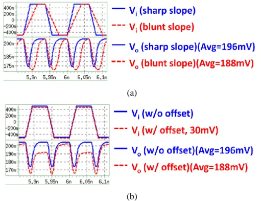
second problem is that the slope detectors are composed with rectifiers which are sensitive to offset. The slope detector is depicted in Fig. 2.12. The inputs are applied to the gate of M1 and M2. The Vo is extracted from the source of M1 and M2. Fig. 2.13(a)
shows the comparison between sharp and blunt slope. The blunt slope has smaller average value (188mV) of Vo. Fig. 2.13(b) shows the comparison between w/o and w/
offset when the slopes are the same value. Because of the offset, Vo has the wrong
average value (188mV) which would be considered as a blunt slope. Thus, the rectifier based slope detector is sensitive to offset.
16
(a)
(b)
Fig. 2.13. The transient response comparison of slope detector. (a) comparison between sharp and blunt slope (b) comparison between w/o and w/ offset
2.3.2 Adaptive equalizer using enhanced low-frequency gain
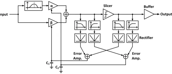
control method [3]
The architecture of adaptive equalizer using enhanced low-frequency gain-control is shown in Fig. 2.14. The adaptive algorithm uses the comparator to generate a reference signal, and collocating with two adaptive loops. The high-frequency loop compares the high-frequency power of EQ filter’s output signal and comparator’s output signal, and then, adjusting the high-frequency gain boost of EQ filter. The low-frequency loop compares the low-frequency power of EQ filter’s output signal and comparator’s output signal, and then controlling the low-frequency gain of EQ filter.
17 Output Input α β Error Amp. Error Amp. C1 C2 Slicer Buffer Rectifier
Fig. 2.14. Architecture of adaptive equalizer using enhanced low-frequency gain-control.
The additional low-frequency loop is design for conquering the drawback of adapting different input swings as the mentioned above.
However, the adaptive loops are still designed with rectifiers. And furthermore, the dual-loop would raise the stability issue.
2.3.3 Adaptive equalizer using direct measurement of the
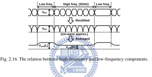
equalizer output amplitude [18]
As depicted in Fig. 2.15, the adaptive algorithm would equalize voltage amplitude of high-frequency and low-frequency components by measuring the equalizer output amplitude. And the output amplitude is measured by a full-wave rectifier which is shown in Fig. 2.16. In the ideal case, the low-frequency components, Vave(L), equal to
VPP, and the high-frequency components, Vave(H), equal to (2/π)×VPP. Hence, the
18 Input Rectifier Control Logic Amp. Gen. CMP 4b 4b CLK Output Buffer
Fig. 2.15. Architecture of adaptive equalizer using direct measurement of the equalizer output amplitude.
VPP
VPP
Low freq. High freq. (3GHz) Low freq.
Recitified
Averaged Vave(L) V
ave(H)
(sin-wave approx.)
Fig. 2.16. The relation between high-frequency and low-frequency components.
However, due to the equalizer is control by digital logic, this may can’t compensate any length of channel. And the algorithm needs external clock to help the digital control schematics, this would raise the design complexity.
2.3.4 Adaptive equalizer with spectrum-balancing technique
As depicted in Fig. 2.17, the adaptive equalizer incorporates spectrum-balancing technique and excludes the requirement of reference signal. The concept of the spectrum-balancing technique utilizes the ratio of high-frequency power over the low-frequency power. The locking condition is when PH=PL, as depicted in Fig. 2.18.
The modified rectifier acts as a power detector, sensing when the power spectrum, and the V/I converter adjusts the gain-boost of the equalizing filter.
19 Input fm fm Rectifier V/I converter Power Detector Output Buffer
Fig. 2.17. Architecture of adaptive equalizer with spectrum-balancing technique.
=0.28 f m T b High-frequency part(PH) Low-frequency part(PL) 10logSx(f) f 1 T b
Fig. 2.18 Spectrum decomposition.
The spectrum balancing technique avoids the DC gain variation and swing issues of previous designs, because it can sense the low-frequency power. However, it requires precise design of the cutoff-frequency in power detector, fm. Furthermore, it’s also
20
Chapter 3
The Design Concept of Slope
Detector
3.1 Motivation
As described above, the detection mechanisms of previous published adaptive equalizers are usually employed with rectifiers. However, the rectifiers [3-4, 17-18] exhibit small detection gain and offset-sensitive. Moreover, they can’t suffer too small input swing, e.g. hundreds millivolts, or, a high-gain error amplifier is required. In addtion, many published detection mechanisms are proposed based on frequency-domain approach. These approaches demand precise frequency
21 Vi Vref2 Vref1 A B C ∆T ∆T Vi Vref2 Vref1 Vi A B C
Fig. 3.1. The operation procedure of slope detector.
characteristics. Thus, we propose a time-domain approach which we call slope-detection technique. As the name called, we detect the slope of signal by the slope detector. With the slope information, we comprehend whether the signal requires more gain-boost.
3.2 The operation procedure of slope detector
Fig. 3.1 shows the operation procedure of slope detector [19-20]. Firstly, the slope detector requires two reference voltages, Vref1 and Vref2. These two reference voltages
compare with input signal (Vi), and then, the signals A and B are produced. The signal C
is obtained from the signals of A and B by XOR gate. We derive the pulsewidth (ΔT) of signal C as:
ref2 ref1 ref
V V V
ΔT= = (3.1)
slope slope
With eq. (3.1), we obtain the slope, or calls edge-speed, of signal. Fig. 3.2 shows the comparison of ΔT between sharp slope and blunt slope. ΔTs is narrower than ΔTb.
22 Vi Vi C Vref1 Vref2 Vref1 Vref2 C
sharp slope blunt slope
∆Tb
∆Ts ∆Ts ∆Tb
Fig. 3.2. The comparison between sharp slope and blunt slope.
Vi
C
Vref1
Vref2
large swing small swing
∆T Vi C Vref1 Vref2 ∆T ∆T ∆T
Fig. 3.3. The comparison between large swing and small swing.
In the adaptive equalizer applications, the input swing would be changed. For example, in USB 3.0 specification, the input swing range of receiver-end would be 400mVp-p to 600mVp-p. Therefore, the adaptive equalizer needs to endure different input
swing. However, when the signals’ swing are different, the signals’ slope are also different, as shown in Fig. 3.3. To obtain the same ΔT when input swings are different. Vref1 and Vref2 require to be adjusted with the different input swing. Hence, the slope
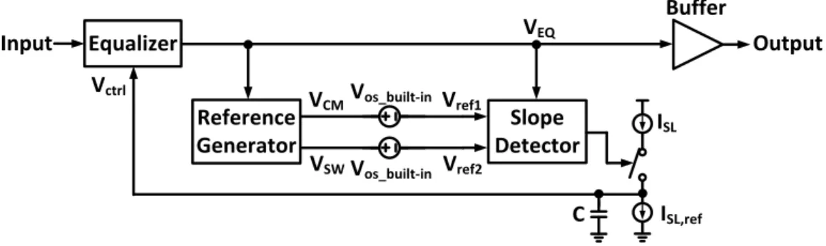
23 Equalizer Vctrl Input VCM VEQ VSW ISL,ref C ISL Vos_built-in Reference Generator Vos_built-in Slope Detector Vref1 Vref2 Buffer Output
Fig. 3.4. The proposed architecture of adaptive equalizer using slope detector.
VCM VSW Vos_built-in Vos_built-in Vref1 Vref2 VEQ C
large swing small swing
∆T ∆T VCM VSW Vos_built-in Vos_built-in Vref1 Vref2 VEQ C ∆T ∆T
Fig. 3.5. The comparison between different swings when Vos_built-in is fixed.
Fig. 3.4 depicts the proposed architecture of adaptive equalizer using slope detector. The reference generator produces VCM and VSW. The slope detector generates the
built-in offset (Vos_built-in) for shifting VCM and VSW to be the Vref1 and Vref2. At last, the
slope information would be transformed to current by the switch and current source. Fig. 3.5 depicts the comparison between different swings when Vos_built-in is fixed. In the
small swing, if the Vos_built-in is too large, ΔT would be the wrong value. Thus, Vos_built-in
need to be smaller than p-p
1
(input swing )
2 for ensuring slope detector detects the correct ΔT. Furthermore, the proper relationship between Vos_built-in and swing is
os_built-in p-p
1
V (input swing )
4
24
I
SL,REFK
EQ,ACI
SL
K
EQ,DCV
OS1V
OS2V
OS3∆V
REFK
INT/s
K
RGK
TIV
CtrlIn
SLIn
SWI
OS5∆T
EQV
OS4SL
EQ
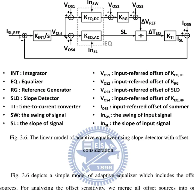
Fig. 3.6. The linear model of adaptive equalizer using slope detector with offset consideration.
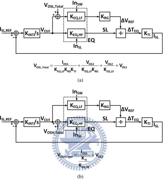
Fig. 3.6 depicts a simple model of adaptive equalizer which includes the offset sources. For analyzing the offset sensitivity, we merge all offset sources into one equivalent offset source, as shown in Fig. 3.7. Fig. 3.7(a) show the equivalent model with input referred offset (VOSL,Total) at the low-frequency path. The ISL is derived as
EQ,LF RG TI INT OSL,Total EQ,LF RG TI EQ,HF SL SL,REF EQ,LF RG TI INT OSL,Total EQ,LF RG TI EQ,HF K K K K V K K K s K I I K K K K 1 V K K K s K
Hence, the sensitive is
OSL,Total EQ,LF RG TI
2 INT 2 INT
EQ,LF RG TI OSL,Total EQ,LF RG TI OSL,Total
EQ,HF EQ,HF SL OSL,Total I V V K K K K K (K K K ) ( V ) (K K K ) ( V ) s K s K Sensitivity
25
I
SL,REFK
EQ,HFI
SLK
EQ,LFV
OSL,Total∆V
REFK
INT/s
K
RGK
TIV
CtrlIn
SLIn
SW∆T
EQSL
EQ
OS5 OS3 OS2
OSL ,Total OS1
EQ ,LF RG TI EQ ,LF RG EQ ,LF I V V V V K K K K K K (a)
I
SL,REFK
EQ,HFI
SLK
EQ,LF∆V
REFK
INT/s
K
RGK
TIV
CtrlIn
SLIn
SW∆T
EQSL
EQ
V
OSH,Total OS5 OSH,Total OS2 TI EQ ,HF I V V K K (b)Fig. 3.7. The linear model for offset sensitivity analysis. (a) the offset effect at low-frequency path (b) the offset effect at high-frequency path
From the above equation, we know KEQ,LF, KRG, KINT and KTI need to be as large as
possible for suppressing the offset effect.
Fig. 3.7(b) show the equivalent model with input referred offset (VOSH,Total) at the
26
V
H,REFK
EQ,HFK
EQ,LFV
OSL1V
OSL2V
OSL3K
INT/s
K
LPIn
ACIn
DCV
OSH1EQ
K
RECV
OSH2V
OSH3K
HPK
RECK
INT/s
V
L,REFV
HV
LV
OSH4V
OSL4K
CTRLFig. 3.8. The linear model of adaptive equalizer using duo-loop control with offset consideration.
EQ,LF RG TI
INT TI
EQ,HF EQ,LF OSH,Total
SL SL,REF
EQ,LF RG TI
INT TI
EQ,HF EQ,LF OSH,Total
K K K K K 1 s K K V I I K K K K K 1 1 s K K V
Hence, the sensitive is
TI
EQ,LF OSH,Total
2 INT EQ,LF RG 2 INT EQ,LF RG
TI TI
EQ,LF EQ,HF OSH,Total EQ,LF EQ,HF OSH,Total
SL OSH,Total I V K 1 K V K K K K K K K 1 K 1 ( ) ( ) ( ) ( ) K s K V K s K V Sensitivity
From the above equation, we know KEQ,LF, KRG, KINT and KTI also need to be as large as
possible for suppressing the offset effect.
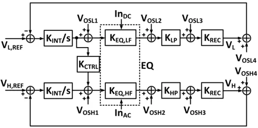
For comparing with the conventional adaptive equalizer, Fig. 3.8 depicted the inear model of adaptive equalizer using duo-loop control [3], which also including the offset consideration. Similarly, all the offset sources are merged in two cases, as shown in Fig. 3.9. In Fig. 3.9(a), VL is derived as
27
V
H,REFK
EQ,HFK
EQ,LFK
INT,H/s
K
LPIn
HFIn
LFEQ
K
RECK
HPK
RECK
INT,L/s
V
L,REFV
HV
OSL,TotalV
LK
CTRLOSL 4 OSL3 OSL2
OSL ,Total OSL1
EQ ,LF LP REC EQ ,LF LP EQ ,LF V V V V V K K K K K K (a)
V
H,REFK
EQ,HFK
EQ,LFK
INT,H/s
K
LPIn
HFIn
LFEQ
K
RECK
HPK
RECK
INT,L/s
V
L,REFV
HV
OSH,TotalV
LK
CTRLOSH4 OSH3 OSH2
OSH,Total OSL ,Total CTRL OSH1
EQ ,HF HP REC EQ ,HF HP EQ ,HF V V V V V K V K K K K K K (b)
Fig. 3.9. The linear model for offset sensitivity analysis. (a) the offset effect at low-frequency path (b) the offset effect at high-frequency path
INT,L
EQ,LF LP REC OSL,Total EQ,LF LP REC
L L,REF
INT,L
EQ,LF LP REC OSL,Total EQ,LF LP REC
K K K K V K K K s V V K 1 K K K V K K K s
28
Hence, the sensitive is
EQ,LF LP REC OSL,Total
2 INT,L 2 INT,L
EQ,LF LP REC OSL,Total EQ,LF LP REC OSL,Total
L OSL,Total V V K K K V K K (K K K ) ( V ) (K K K ) ( V ) s s Sensitivity
From the above equation, we know KEQ,LF, KLP, KREC and KINT need to be as large as
possible for suppressing the offset effect.
Fig. 3.9(b) show the equivalent model with input referred offset (VOSH,Total) at the
high-frequency path. The VH is derived as
INT,H
EQ,HF HP REC EQ,HF HP REC OSH,Total
H H,REF
INT,H
EQ,HF HP REC EQ,HF HP REC OSH,Total INT,L CTRL EQ,HF HP REC L,REF INT,L EQ,LF LP REC K K K K K K K V s V V K 1 K K K K K K V s K K K K K s V K 1 K K K s
Hence, the sensitive is
EQ,HF HP REC OSH,Total
2 INT,H 2 INT,H
EQ,HF HP REC OSH,Total EQ,HF HP REC OSH,Total
H OSH,Total V V K K K V K K (K K K ) ( V ) (K K K ) ( V ) s s Sensitivity
From the above equation, we know KEQ,HF, KHP, KREC and KINT also need to be as large
as possible for suppressing the offset effect.
However, the KREC is quite small in this adaptive mechanism. Thus, our proposed
29
Chapter 4
A
13.5Gb/s
Positive-Feedback
based Adapative Equalizer with
Large Input Dynamic Range Using
Offset-Insensitive Slope Detector
4.1 Motivation
With the progress in communication transmission, the operation data rate increases up to tens of Gb/s is the predictable trend in the future days. The power consumption is important issues in the schematic design, especially the equalizer schematic. This work proposes a positive-feedback based equalizer which regenerating gain at high-frequency for saving power consumption. Moreover, to decrease area consumption, the equalizer doesn’t use inductive peaking technique.
30
4.2 Specification
2 4 6 8 10 -30 -25 -20 -15 -10 -5 0 M a g n it u d e (d B ) Frequency(GHz) 18-inch (a) (b)Fig. 4.1. (a) The magnitude response of 18-inch channel (b) The Transient response of 18-inch channel
In this work, we utilize 65nmCMOS technology. Due to the testing instruments limitations, the data rate is set at 16Gb/s. The channel loss of 18-inch is 21dB at 8GHz, as shown in Fig. 4.1. Fig. 4.2 shows the eye-diagram under 18-inch.
We utilizes four cascaded differential pair to compensate 21dB channel loss, and the reverse scaling technique [16] are used. We compare the performance between with and without revers scaling, as shown in Fig 4.2. In Fig. 4.2(b), the reverse scaling factor
31
C
1
1
1
1
(a)C
1
2
4
8
(b)Fig. 4.2. Cascading four differential pairs to compensate 18-inch channel. (a) Without reverse scaling technique
(b) With reverse scaling technique
Table 4.1 The comparison between without and with reverse scaling.
w/o reverse scaling
w/ reverse scaling
DC-Gain*
1
1
Bandwidth*
0.56
1
Output noise*
2
1
Power*
0.27
1
* Normalized based on the value of w/ reverse scaling
is 2. Table 4.1 shows the overall performance of Fig. 4.2 (a) and (b). It reveals the revers scaling technique can provide better bandwidth and noise performance.
32
4.3 Circuit Design
4.3.1 Equalizer
Vo(s) Vi(s) H(s) VH(s) A(s)Fig. 4.3. The block diagram of positive-feedback system.
Vo(s) Vi(s) H(s) VH(s) Gm1(s) Gm1(s) Zo(s) Gm2(s)
Fig. 4.4. The improved positive-feedback system.
Fig. 4.3 shows a basic positive-feedback system. For more detail analysis in the positive-feedback, the adder and A(s) are replaced by Gm1(s) and Zo(s), as shown in Fig.
4.4. The transfer function is derived as
o m1 o m1 o i m1 o m2 o V (s) 1 1 G (s) Z (s) G (s) Z (s) (4.2) V (s) 1G (s) H(s) Z (s) 1G (s) Z (s)
where Gm1(s) and H(s) are merged as Gm2(s). As long as Gm2(s) ‧Zo to be close to 1, the
closed-loop gain reaches infinity. For example, if Gm1(s)‧Zo(s) is 1, as long as Gm1(s)‧
Zo(s) is 0.5, the gain would be 2. Unlike RC degeneration technique, the DC-gain need
33 Vi RD RD M1 M2 Vo M3 M4 CS Gm1(s) Gm2(s) Zo Freq. ωz ω0 Vo Vi Vb M6 M7 M5 (a) RD M1,2 Vo CL1 M3,4 CL2 Vi (b)
Fig. 4.5. (a)The basic implemented schematic and magnitude response of positive-feedback based equalizer. (b) the half-circuit of (a)
A basic schematic of the positive-feedback based equalizer is implemented, as shown in Fig. 4.5(a). M1, M2and M5 realize Gm1(s). M3, M4, M6, M7 and CS realize
Gm2(s). And the Zo is realized by RD and Cp. From Fig. 4.5(b), we derive the transfer
function as : m1,2 o z 2 0 2 i L1 0 m3,4 m3,4 z 0 s L2 L2 s L2 m3,4 D L1 s L2 m3,4 D s L2 0 L2 s L2 g V (s) s (4.3) V (s) C s s Q g g , 2C C C (2C C ) g R C (2C C ) g R (2C C ) Q C (2C C )
34
where gm1,2 means the transconductance of M1 and M2, gm3,4 means the
transconductance of M3 and M4, gds6,7 means the reciprocal of M6 and M7’s output
resistor, CL1=Cgd1,2+4Cgd3,4+Cp,Vo, CL2 =2Cgs3,4+Cgd6,7+2Cs+Cp,Vs3,4. As the transfer
function showing, not only ωz provide peaking, but also complex poles (Q) generate
peaking. As the magnitude response showing in Fig. 4.5, ωz provides low-frequency
gain-boost and the complex poles (Q) provide gain-boost at high-frequency.
Considering the stability of positive-feedback, the complex poles’ real parts couldn’t be positive. The complex poles are derived as
2 2 0 0 0 ( ) (2 ) Q Q s 2 Thus, m3,4 D L1 s L2 m3,4 D s L2 0 L2 s L2 s L2 s L2 m3,4 D s L2 L1 s L2 L1 m3,4 D g R C (2C C ) g R (2C C ) 0 Q C (2C C ) 2C C 2C C g R , where 1 2C C C 2C C C g R 1
Hence, as long as gm3,4RD1, ω0/Q would be larger than 0. This can confirm the
35
VEQ
Gain Stage VIN
Fig. 4.6. Block diagram of Equalizer.
Freq.
DC Gain=g
m1,2R
DV
iR
DR
DM
2M
1V
oR
GR
GC
GC
GR
MatchR
MatchV
G Vo ViC
pC
pω
zgω
pg1ω
pg2Fig. 4.7. The schematic and magnitude response of gm-boosted technique.
Fig. 4.6 depicts the proposed equalizer which is composed with five stages, including four peaking stages and one gain stage. The first four stages providing about 20dB gain-boost, and the last stage operates as a buffer to decreasing the loading effect. The first stage not only uses positive-feedback based equalizer, but also utilizing the gm-boosted technique [21-22] for providing large peaking at high frequency. This stage has a 8dB of gain-boost at 8GHz. The second stage combines RC degeneration technique with positive-feedback based technique. It also has a 8dB of gain-boost at 8GHz. The third stage only utilizes positive-feedback based technique, which provides a 6dB of gain-boost at 8GHz. The fourth stage also uses positive-feedback based technique, however, it provides low-frequency gain-boost and delay equalization. The fifth stage operates as a buffer to isolate the loading effect from the following circuits.
36
V
iR
DR
DM
2M
1V
oC
LC
LM
3M
4C
SV
ctrlR
GR
GC
GC
GR
MatchR
MatchV
Gω
Z,pfω
0,pf V o Viω
Z,gFreq.
ω
P,g1Fig. 4.8. The schematic and magnitude response of the first stage.
V
iR
DR
DM
1M
2V
oC
LC
LV
ctrlR
SC
S1C
S2M
3M
4ω
z,pfω
0,pf Vo Viω
z,cdFreq.
ω
p,cdFig. 4.9. The schematic and magnitude response of the second stage.
function is derived as:
z,g o m1,2 D i p1,g p2,g z,g p1,g p2,g G G G G D L (s ) V (s) 2g R (4.4) 1 1 V (s) (s )(s ) 1 1 1 , , 2R C R C R C
37 2 4 6 8 10 0 2 4 6 8 10 12 M a g n it u d e (d B ) Frequency(GHz) (a) 2 4 6 8 10 -4 -2 0 2 4 6 M a g n it u d e (d B ) Frequency(GHz) (b) 2 4 6 8 10 -2 0 2 4 6 M a g n it u d e (d B ) Frequency(GHz) (c)
Fig. 4.10. The magnitude response of the first three stage. (a) the first stage (b) the second stage (c) the third stage
38
shown in Fig. 4.7, which ωp1,g is two times of ωz,g. Moreover, the gm-boosted technique
can only utilized at the first stage, due to the input node is a low input impedance. The proposed schematic of first stage is shown in Fig. 4.8. The RMatch is designed for
matching 50Ω impedance of the instrument. ωz,pf and ωz,g are designed at 3.6GHz and
6.8GHz. And, the Q is about 2.5. Fig. 4.9 shows the schematic of the second stage. In this stage, ωz,pf and ωz,cd are designed at 4GHz and 6GHz. And, the Q is about 2.3. The
third and the fourth stages use the basic schematics of positive-feedback based equalizer, which has been shown in Fig. 4.5. In the third stage, ωz,pf is designed at 5GHz. And,
the Q is about 2. The simulated magnitude response of the first three stages are shown in Fig. 4.10. As described above, the first stage provides 8dB of gain-boost, the second stage provides 8dB of gain-boost, and the third stage provides 6dB of gain-boost.
Specifically, the fourth stage is designed for both magnitude and delay equalization [23]. Due to Q is utilized in the previous stages for large gain-boost at high-frequency, the group-delay has large difference between low-frequency and high-frequency. According to eq. (4.3), the transfer function of fourth stage is derived as, we set sn=s/ωo,: m1,2 o n n 0 z 2 0 2 i n p n 0 n 0 0 g V (s ) s (4.5) V (s ) C s s Q
And then from above equation, we know :
1 n 0 1 n n 2 z n / Q ( ) tan ( ) tan ( ) (4.6) 1
We do differentiation on θ(ωn) to get delay : 2 n n z n 2 2 2 2 2 0 n n z n 0 2 2 n n 2 2 2 2 2 2 2 n 0 0 n n 0 n n z z d ( ) 1 (1 / Q)(1 ) D( ) (4.7) d (1 ) ( / Q) ( ) 1 (1 / Q)(1 ) 1 1 (1 / Q)(1 ) ( ) (1 ) ( / Q) (1 ) ( / Q)
39 Normalized Frequency Normalized Delay of D(ωn) increasing Q ωn=1
Fig. 4.11. The normalized delay response of equalizer.
As the above equation showing, we get the maximum delay when n n dD(ω ) 0 dω . At this time, 2 n 1 4 Q 1 , when Q>1 Finally, when n 1, max 0 2Q D Q (4.8)
That is to say, if we want more delay, the Q needs to be larger as shown in Fig. 4.11. in our design, the ωo is designed at low frequency to decrease the group-delay difference.
Fig. 4.12 shows the magnitude and group delay response of fourth stage. The peaking is designed at 1.8GHz, and the maximum delay equalization isdesigned at 0.5GHz.
Fig. 4.13 and Fig. 4.14 show the comparison between with and without the fourth stage when the channel has been compensated by the previous three stages. When the channel is equalized with the fourth stage, not only the magnitude response is compensated well, but also group delay is improved with less difference between low-frequency and high-frequency. Thus, the eye-diagram is also recovered well with less jitter.
40 2 4 6 8 10 -2 -1 0 1 2 3 4 M a g n it u d e (d B ) Frequency(GHz) (a) 2 4 6 8 10 0 2 4 6 8 10 M a g n it u d e (d B ) Frequency(GHz) (b)
Fig. 4.12. (a) Magnitude response of the fourth stage. (b) Group delay response the fourth stage.
41 2 4 6 8 10 -8 -6 -4 -2 0 2 M a g n it u d e (d B ) Frequency(GHz)
with the fourth stage without the fourth stage
(a) 2 4 6 8 10 20 22 24 26 28 30 32 34 G ro u p d e la y (p s ) Frequency(GHz)
with the fourth stage without the fourth stage
(b)
42
(a)
(b)
Fig. 4.14. Eye-diagrams comparison (a) without the fourth stage (b) with the fourth stage Vi RD RD M1 M2 Vo Cp Cp
Fig. 4.15. The schematic and magnitude response of the fifth stage.
At last, the schematic of the fifth stage is depicted in Fig. 4.15. It decreases the parasitic effect from next stage (detection schematics).
43 2 4 6 8 10 -5 0 5 10 15 20 25 M a g n it u d e (d B ) Frequency(GHz) Vctrl=0V Vctrl=0.3V Vctrl=0.6V Vctrl=0.9V
Fig. 4.16. The magnitude response of equalizer under different Vctrl.
Fig. 4.16 shows the simulated magnitude response of equalizer under different Vctrl.
It provides about 22.5dB at 8GHz under Vctrl=0V.
4.3.2 Common-mode Detector
The schematic of common-mode detector is depicted in Fig. 4.17. It utilizes the differential signal, VEQ+ and VEQ-, to cancel the input feedthrough signal from each other,
and then only keeps the DC information of signal by low-pass filter.
R
C R
VCM
VEQi+ V
44
4.3.3 Swing Detector
VEQ M1 M2 M3 M4 M5 M6 M8 VSW VB_OS ICh CL VSW,ref M7Fig. 4.18. The schematic of swing detector.
VEQ
VSW
ΔVDis
ΔVCh
(Charging mode) (Discharging mode)
tCharging tDischarging
Fig. 4.19. The relation of VEQ and VSW.
The circuit of swing detector is depicted in Fig. 4.17 [24] , it’s improved from previous paper [25-26] which is called peak detect and hold (PDH) circuit. The VSW
would follow the VB_OS by the source follower (M8). As the Fig. 4.18 showing, when the
swing detector is in charging mode, the increased voltage of VSW is ΔVCh. ΔVCh can be
calculated as : Ch Ch Ch arg ing L I V t (4.9) C
And during holding mode, the ΔVDis can be calculated as :
Disch arg ing VB _ OS t Dis B _ OS V V (0)(1 e ) (4.10)
45 2 4 6 8 10 -10 0 10 20 30 M a g n it u d e (d B ) Frequency(GHz) (a) 2 4 6 8 10 -280 -260 -240 -220 -200 -180 -160 P h a s e (d e g re e ) Frequency(GHz) (b)
Fig. 4.20. (a) Magnitude response of swing detector. (b) Phase response comparison of swing detector.
tDischarging followed by 1-bit tCharging. At this time, VSW (VB_OS) would have the maximum
error voltage. For a PRBS7 data pattern with 16Gb/s data rate. The long tDischarging is
46 200 300 400 500 0.96 1.00 1.04 1.08 1.12 1.16 V o lt a g e (V ) Input swingp-p(mV) Expected VSW Simulated VSW
Fig. 4.21. The relations between input swingp-p, expected VSW
and simulated VSW.
smaller than 10%, we can derive the VB _ OS as, by eq. (4.10), : Disch arg ing
B _ OS B _ OS t Dis B _ OS(0) V V (1 e ) 10% V 4.16ns
Thus, ro7 can be a quite large value. And moreover, to save the power consumption, the
ID7 is designed to be a few-micro Amperes which also increases ro7. Fig. 4.19 and Fig.
4.20 shows the open-loop magnitude and phase response of swing detector. The phase margin has 94 degree which is a one-pole system. Fig. 4.21 shows the relations between input swingp-p, expected VSW and simulated VSW. The simulated VSW is almost the same