國 立 交 通 大 學
電子工程學系電子研究所
博 士 論 文
高介電係數介電質與金屬閘極製程技術之研究與
應用
The Investigation and Application of High-κ
Dielectrics and Metal Gate Process Technologies
研 究 生 :洪彬舫
指導教授 :荊鳳德 博士
高介電係數介電質與金屬閘極製程技術之研究與
應用
The Investigation and Application of High-κ
Dielectric Metal Gate Process Technologies
研 究 生:洪彬舫 Student: Bing-Fang Hung
指導教授:荊鳳德 Advisor: Dr. Albert Chin
國立交通大學
電子工程學系電子研究所
博士論文
A Dissertation
Submitted to Department of Electronics Engineering &
Institute of Electronics
College of Electrical and Computer Engineering
National Chiao Tung University
in Partial Fulfillment of the Requirements
for the Degree of Doctor of Philosophy
In
Electronics Engineering
2006
Hsinchu, Taiwan, Republic of China
i
高介電係數介電質與金屬閘極製程技術之研究
與應用
研究生:洪彬舫 指導教授:荊鳳德教授
國立交通大學
電子工程學系暨電子研究所
摘要
隨著互補式金氧半電晶體(CMOS)元件尺寸持續微縮,傳統的絕緣層-二氧化 矽(SiO2)將遭遇漏電流過大的物理限制。另外,傳統的多晶矽閘極也將遭遇諸多 挑戰-多晶矽空乏、硼穿透及高電阻係數。因此,新的絕緣層及閘極材料將是往 後幾年超大型積體電路(VLSI)發展極需解決的問題。近年來,高介電係數介電層 與金屬閘極的技術發展,已成為半導體產業最重要的研究之一。在本論文中,吾 人將探討數種高介電係數介電層與金屬閘極的研究與應用。 首先,我們將探討高介電係數氮氧化矽鉿(HfSiON)介電層,分別選用矽化鉿(HfSix)與矽化銥(IrxSi)所形成的全金屬矽化閘極(FUSI)來當 n-型與 p-型金氧半場
效電晶體的閘極。而氮氧化矽鉿雖然比氧化鉿有較低的介電係數,但卻有較佳的
熱穩定性。另外,使用矽化鉿與矽化銥全金屬矽化閘極比純金屬閘極有更好的熱
現象。結果顯示,結合氧化矽鉿與矽化鉿與矽化銥全金屬矽化閘極,是實現雙金 屬閘極互補式金氧半電晶體很好的選擇之一。 其次,我們將探討另一種高介電係數介電層氮氧化鑭鉿(HfLaON),結合金 屬氮化物閘極氮化鉭(TaN)應用於 n-型金氧半場效電晶體。氮氧化鑭鉿與氮氧化 矽鉿同樣具有良好的高溫熱穩定性,但氮氧化鑭鉿卻有比氮氧化矽鉿還要高的介 電係數的優點。此外,氮化鉭閘極具有良好的高溫熱穩定性,且結合氮氧化鑭鉿 介電層後,其有效功函數將可調變到適用於n-型金氧半場效電晶體的應用。 最後,我們將高介電係數氧化鑭鋁(LaAlO3)應用於低溫複晶矽薄膜電晶體
(Low Temperature poly-Si TFTs)並結合低功函數鐿(Yb)金屬閘極,可以有效降低
有效氧化層厚度(EOT)來達成提升電流密度及降低臨界電壓,進而得到大的驅動
電流元件特性。此良好的元件特性並無經過氫化及特殊再結晶製程,且將可應用
iii
The Investigation and Application of High-κ
Dielectrics and Metal Gate Process Technologies
Student: B. F. Hung Advisor: Dr. Albert Chin
Department of Electronics Engineering
& Institute of Electronics
National Chiao Tung University
Abstract
To continue down-scaling CMOS technology, traditional insulator layer - SiO2
will face the physical limitation - large gate leakage current. In addition, traditional
poly-Si gate encounters several inherent limitations, such as poly-Si depletion, boron
penetration, and high resistivity. Therefore, new insulator and gate material
technologies will become urgent for very large scale integration (VLSI) technology in
the future years. Recently, metal-gate/high-κ process technologies become one of the
most important researches in the semiconductor industry. In this dissertation, we will
investigate the application of several high-κ dielectric and metal gate process
technologies.
First of all, we will study the application of HfSiON dielectric with HfSix and
IrxSi full silicidation (FUSI) metal gates in n-MOSFETs and p-MOSFETs,
thermal stability. Besides, using HfSix and IrxSi FUSI metal gates can obtain better
thermal stability than using pure metal gates, and also can reduce the effective work
function shifts due to Fermi-level pinning effect. These results indicate that
integrating HfSiON with HfSix and IrxSi FUSI metal gates can achieve dual metal
gates development in CMOS technology.
Next, we will study another high-κ dielectric HfLaON with metal nitride TaN gate
in n-MOS application. HfLaON has good thermal stability as HfSiON, but it has the
advantage of higher κ value. Moreover, TaN also has similarly good thermal stability.
Integrating HfLaON with TaN gate will provide the appropriate effective work
function in n-MOS application.
Finally, the application of high-κ LaAlO3 dielectric into low-temperature poly-Si
thin-film transistors (TFTs) combining with low work function Yb metal gates was
investigated. Good TFT performance was achieved - such as a high drive current and
low threshold voltage due to the down-scaling effective oxide thickness (EOT)
provided by the high-κ dielectric. In addition, the good performance was achieved
without hydrogen passivation or special crystallization steps. These results suggest
that the Yb/LaAlO3 TFTs can meet the device requirements for system-on-panel (SOP)
v
Acknowledgement
First of all, I would like to thank my advisor Prof. Albert Chin for his fruitful
discussions and illuminative suggestions during the period of my working toward phD
degree. His inspiration benefits me a lot on the creative ideas, effective schedule
control and the integrity to the processing tasks. I am also grateful to ED633 group
members - Dr. C. H. Huang, Dr. M. Y. Yang, Dr. D. S. Yu, Dr. C. C. Chen, Dr. H. L.
Kao, Dr. C. H. Lai, C. H. Wu, K. C. Chiang, C. F. Cheng, C. C. Huang, Terry Wang, Z.
W. Lin and W. L. Huang, for their enthusiastic assistance and cooperation.
Moreover, I am appreciative of the financial and equipment supports form
National Science Council, National Nano Device Lab (NDL), and Semiconductor
Center of NCTU. I am also grateful to those who ever assisted this work.
Finally, I greatly appreciate my parents, family, and my dear girl friend Miss
Chia-Chin Hsieh who always support me and give me endless encouragement and
Contents
Abstract (in Chinese)……….……….……….………i
Abstract (in English) ………..……….……….………….…iii
Acknowledgement……….v
Contents……….……….………….……vi
Table Captions……….……….……….…viii
Figure Captions……….……….……….……ix
Chapter 1 Introduction
1.1
Overview of high-κ gate dielectrics……….……….11.2
Overview of metal gate electrodes……….……….21.3
Innovation and contribution…………...….……….41.4
Thesis Organization…………...…….……….6References……….………...………….……….7
Chapter 2 High temperature stable Ir
xSi Gates with High Work
Function on HfSiON p-MOSFETs
2.1
Introduction……….………..……142.2
Experimental procedure………...……….162.3
Results and discussion……….……….…….………172.4
Conclusion……….………20References……….……….………...………..….………….22
Chapter 3 HfSiON n-MOSFETs Using Low Work Function HfSi
xvii
3.2
Experimental procedure………....………...…………333.3
Results and discussion…………..……….…………343.4
Conclusion………..……….…..……35References……….……….…….………...………..….………….37
Chapter 4 Novel High-
κ HfLaON n-MOSFETs with Preserved
Amorphous State to 1000
oC
4.1
Introduction………….………..………..…454.2
Experimental procedure.………..………..…464.3
Results and discussion………..………...………..………474.4
Conclusion………...………..……50References……….……….…….………...………..….………….51
Chapter 5 Poly-Silicon Thin Film Transistors Using Ytterbium
Metal Gate and LaAlO
3Dielectric
5.1
Introduction………..………...………..……695.2
Experimental procedure……….…………..………..………705.3
Results and discussion………..………715.4
Conclusion……….……….………..…73References……….……….…….………...………..….………….74
Chapter 6
Conclusions……….………82Vita………..………..……..……84
Table Captions
Chapter 5 Poly-Silicon Thin Film Transistors Using Ytterbium
Metal Gate and LaAlO
3Dielectric
Table 5-1 Comparison of poly-Si TFTs formed by a furnace-crystallization with
various gate dielectrics of LaAlO3, Al2O3, LPCVD SiO2, and PECVD
ix
Figure Captions
Chapter 1 Introduction
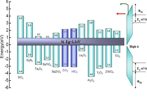
Fig. 1-1 The evolution of CMOS technology requirements (ITRS 2005).
Fig. 1-2 The band offset of popular high-κ materials.
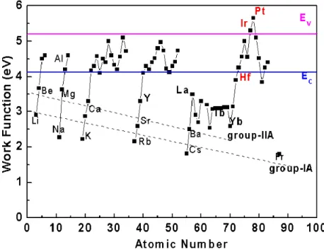
Fig. 1-3 The values of work function for different metal materials.
Chapter 2 High temperature stable Ir
xSi Gates with High Work
Function on HfSiON p-MOSFETs
Fig. 2-1 C-V characteristics of HfSiON/n-Si with IrxSi, Ir and Al gates capacitors.
The device areas are 100 μm × 100 μm.
Fig. 2-2 J-V characteristics of HfSiON/n-Si with IrxSi, Ir and Al gates capacitors.
Fig. 2-3 XRD profiles of Ir3Si/HfSiON structures.
Fig. 2-4 SIMS profile of Ir3Si gates on HfSiON at different RTA temperature. The
Ir3Si accumulated toward HfSiON interface is found to un-pin the
Fermi-level.
Fig. 2-5 The Id-Vd characteristics of Ir3Si/HfSiON p-MOSFETs.
Fig. 2-6 The Id-Vg characteristics of Ir3Si/HfSiON p-MOSFETs.
Fig. 2-7 The extracted hole mobilities from Id-Vg characteristics of Ir3Si/HfSiON
Chapter 3 HfSiON n-MOSFETs Using Low Work Function HfSi
xGates
Fig. 3-1 C-V characteristics for high temperature RTA formed HfSix/HfSiON and low temperature Al/HfSiON capacitors. The device area was 100 μm×100
μm.
Fig. 3-2 J-V characteristics for high temperature RTA formed HfSix/HfSiON and
low temperature Al/HfSiON capacitors.
Fig. 3-3 The Id-Vd characteristics of HfSix/HfSiON n-MOSFETs. The
amorphous-Si on HfSiON was 5 nm and gate length was 10 μm.
Fig. 3-4 The Id-Vg characteristics HfSix/HfSiON n-MOSFETs. The amorphous-Si
on HfSiON was 5 nm and gate length was 10 μm.
Fig. 3-5 The electron mobilities of HfSix/HfSiON n-MOSFETs.
Chapter 4 Novel High-
κ HfLaON n-MOSFETs with Preserved
Amorphous State to 1000
oC
Fig. 4-1 Grazing incident XRD spectra of HfLaO after different RTA temperature.
Fig. 4-2 Grazing incident XRD spectra of HfLaON with NH3 plasma after different
RTA temperature. In contrast to the HfLaO case, HfLaON stays
xi
Fig. 4-3 XPS spectra of HfLaON after 1000oC RTA. The existence of Hf, La, O,
and N is clearly seen.
Fig. 4-4 TEM image of TaN/HfLaON/Si after 1000oC RTA. Good interface
property is observed with very thin interfacial layer.
Fig. 4-5 J-V characteristics of 1000oC-annealed TaN/HfLaON n-MOS capacitors
with various N+ nitridation.
Fig. 4-6 C-V characteristics of 1000oC-annealed TaN/HfLaON n-MOS capacitors
with various N+ nitridation.
Fig. 4-7 C-V characteristics of TaN/HfLaON n-MOS capacitors after different
temperature RTA. The device area was 100 μm×100 μm.
Fig. 4-8 J-V characteristics of TaN/HfLaON n-MOS capacitors after different
temperature RTA.
Fig. 4-9 SIMS profile of TaN gate on HfLaON at different temperature RTA. No Ta
penetration through HfLaON can be found.
Fig. 4-10 The comparison of gate leakage current density for MOS devices with
SiO2 and HfLaON gate dielectrics.
Fig. 4-11 The dielectric constant of HfLaON at different RTA temperature.
Significant higher κ value at high RTA temperature is obtained than HfO2.
1000oC RTA thermal cycle.
Fig. 4-13 The Id-Vg characteristics of TaN/HfLaON n-MOSFETs fabricated at
1000oC RTA thermal cycle.
Fig. 4-14 The electron mobilities of TaN/HfLaON n-MOSFETs fabricated at 1000oC
RTA thermal cycle.
Fig. 4-15 The ΔVt of TaN/HfLaON n-MOSFETs stressed at 85oC and 10 MV/cm
for 1 hour.
Chapter 5 Poly-Silicon Thin Film Transistors Using Ytterbium
Metal Gate and LaAlO
3Dielectric
Fig. 5-1 C-V hysteresis of 50 nm LaAlO3 gate dielectric with 400oC 30 min furnace
O2 treatment after sweeping between 5V and -5V. The ΔVhys is smaller
than 70 mV.
Fig. 5-2 The gate current density vs. electric field relation for LaAlO3 gate dielectric
poly-Si TFT.
Fig. 5-3 The Id-Vg characteristics of the Yb/LaAlO3 poly-Si TFT measured at Vds =
0.1 V.
Fig. 5-4 The Id-Vd characteristics of the Yb/LaAlO3 poly-Si TFT.
1
Chapter 1
Introduction
1.1 Overview of high-κ gate dielectrics
The gate leakage current through the gate oxide increases significantly because direct tunneling is the primary conduction mechanism in down-scaling CMOS
technologies. To reduce the leakage current related higher power consumption in
highly integrated circuit and overcome the physical thickness limitation of silicon
dioxide, the conventional SiO2 will be replaced with high dielectric constant (high-κ)
materials as the gate dielectrics beyond the 65 nm technology mode [1]-[6]. Therefore,
the engineering of high-κ gate dielectrics have attracted great attention and played an
important role in VLSI technology. Although high-κ materials often exhibit smaller
bandgap and higher defect density than conventional silicon dioxide, using the high-κ
gate dielectric can increase efficiently the physical thickness in the same effective
oxide thickness (EOT) that shows lower leakage characteristics than silicon dioxide
by several orders without the reduction of capacitance density [2]-[5]. According to
the ITRS (International Technology Roadmap for Semiconductor) [7], the suitable
gate dielectrics must have κ value more than 8 for 50-70 nm technology nodes and
shows the evolution of CMOS technology requirements.
Research on finding an appropriate substitute to the superior SiO2 has been going
on for almost a decade. Oxy-nitrides (SiOxNy) have been introduced to extend the use
of SiO2 in production but eventually it has to be replaced by a high-κ material, such as
Ta2O5,TiO2, HfO2, ZrO2, Al2O3, La2O3 or mixtures of them or metal-oxide-silicates of
the mentioned compounds. However, most metal oxides will have the characteristics
of crystallization at elevated temperature which cause devices generate non-uniform
leakage distribution and give large statistical variation for nano-meter devices across
the chip. Therefore, replacement gate strategies have been proposed to prevent
crystallization and deleterious effects of mass and electrical transport along grain
boundaries. Fig. 1-2 shows the summaries of the κ value and band offset for popular
high-κ dielectric candidates.
1.2 Overview of metal gate electrodes
The gate electrode in CMOS devices is conventionally made of highly doped
polycrystalline silicon (poly-Si). However, as the CMOS technology down-scaling,
poly-Si gate will encounter several inherent limitations. One of them is depletion of
the poly-Si electrode when the gate stack is biased in inversion [8]-[20]. The depleted
region is added to the dielectric thickness, which results the increase of EOT and
3
is another issue due to the scaling geometry. Besides, diffusion of boron penetrates
from the poly-Si gate will also degrade the performance of the transistors.
To overcome these problems, using metal gate electrodes will be a practical way
to eliminate poly gate depletion and boron penetration [8]-[15]. In addition, metal
gates also show the potential of reduced sheet resistance. However,
metal-gate/high-κ CMOSFETs show undesired high threshold voltages (Vt), which is
opposite to the VLSI scaling trend. This phenomenon is known as “Fermi-level
pinning”, although the background physics may be attributed to interface dipole
and/or charged defects [8]. Moreover, thermal stability of the effective metal electrode
and metal diffusion are also important considerations.
The work functions (Φm) of metal shown in Fig. 1-3 play an important role for
metal-gate/high-κ CMOSFETs. The preferred work function of the metals are ~5.2 eV
for p-MOSFETs and ~4.1 eV for n-MOSFETs. Recently, lots of metal or metal-nitride
materials have been widely researched and successfully intergraded in advanced
CMOSFETs, such as TiN, TaN, Pt, Mo and Ir [8]-[20]. However, it has been found
that thermal annealing of the metal gates at temperatures above 900oC results in
mid-gap values for almost all metal gate candidates. Therefore, the Fermi-level
pinning effect needs to be avoided by selecting suitable metal gate and high-κ
1.3 Innovation and Contribution
To compensate Fermi-level pinning effect, low and high work function metal
electrodes are required to reduce the pinning effect for n- and p-MOSFETs,
respectively. For p-MOSFETs, high work function metal electrodes larger than the 5.2
eV of p+ poly-Si are needed. However, only Ir (5.27 eV) and Pt (5.65 eV) in the
Periodic Table [21] can meet this requirement, which make the
metal-gate/high-κ p-MOSFETs especially challenging [8]-[10]. Ir is more preferable
than Pt due to a simpler etching process by reactive ion etching (RIE) [22]-[23].
Unfortunately, large metal diffusion through high-κ dielectrics was found in pure Ir
gates after 1000oC RTA which caused p-MOS device failures [24]-[25]. Another
possibility is using low temperature full silicidation (FUSI) gates [9],[24]-[27].
However, the p-MOS devices incorporating high work function PtxSi or IrxSi still
failed to integrate into the CMOS SALICIDE process due to the lack of required
selective wet etching of Pt or Ir during SALICIDE. In this thesis, we have proposed
and demonstrated a new high temperature stable IrxSi FUSI gate on high-κ HfSiON
with a proper effective work function of 4.95 eV. HfSiON has good metal diffusion
barrier property and the good compatibility with currently used SiON gate dielectric
with added Hf for higher κ value.
5
develop the low work function HfSix gate for n-MOSFETs. This is because the Hf has
very low work function of 3.5 eV in the Periodic Table. The HfSix gate on HfSiON,
formed by Hf deposition on thin amorphous Si, gives a low effective work function of
4.27 eV. In addition, the HfSix/HfSiON can sustain a high rapid thermal annealing
(RTA) temperature of 1000◦C that is compatible with current VLSI process line.
Since both process and mechanism of HfSix and IrxSi, with respective low and high
effective work function, are the same, these results indicate the high possibility to
realize dual work function metal-gate/high-κ CMOS with large work function
difference.
Besides, we also developed the novel HfLaON gate dielectric with simple TaN
metal gate, good device integrity with a low effective work function of 4.24 eV has
been obtained for n-MOSFETs. The preserved 1000oC amorphous state is similar to
currently used SiO2 or SiON, with additional merit of full process compatibility with
VLSI fabrication lines.
Finally, we have integrated low work function ytterbium (Yb) metal gate with
high-κ LaAlO3 dielectric into low-temperature poly-Si (LTPS) thin film transistors
(TFTs). Good TFT performance was achieved - such as a high drive current, low
threshold voltage and sub-threshold slope, as well as an excellent on/off current ratio
passivation or special crystallization steps. The good performance is related to the
high gate capacitance density and small equivalent-oxide thickness provided by the
high-κ dielectric.
1.4 Thesis Organization
This dissertation focused on the characterization of alternative metal gates and
high-κ dielectric materials for the sub-45 nm technology node. In this chapter, the
history of high-κ dielectrics and metal gate electrode evolution and the key materials
have been reviewed. Chapter 2, 3, and 4 deeply study the IrSix gate on HfSiON for
p-MOS, HfxSi gate on HfSiON for n-MOS, TaN gate on HfLaON for n-MOS,
respectively. Chapter 5 presents the study of Yb metal gate combining with a high-κ
LaAlO3 dielectric into low-temperature poly-Si TFTs. A summary and suggestion are
7
Reference
[1] M. Koyama, K. Suguro, M. Yoshiki, Y. Kamimuta, M. Koike, M. Ohse, C. Hongo and A. Nishiyama, “Thermally stable ultra-thin nitrogen incorporated ZrO2 gate dielectric prepared by low temperature oxidation of ZrN,” in IEDM
Tech. Dig., pp. 20.3.1-20.3.4, 2001.
[2] E. P. Gusev, D. A. Buchanan, E. Cartier, A. Kumar, D. DiMaria, S. Guha, A. Callegari, S. Zafar, P. C. Jamison, D. A. Neumayer, M. Copel, M. A. Gribelyuk, H. Okorn-Schmidt, C. D Emic, P. Kozlowski, K. Chan, N. Bojarczuk, L. -A. Ragnarsson and Rons, “Ultrathin high-κ gate stacks for advanced CMOS devices,” in IEDM Tech. Dig., pp. 20.1.1-20.1.4, 2001.
[3] W. Zhu, T. P. Ma, T. Tamagawa, Y. Di, J. Kim, R. Carruthers, M. Gibson and T. Furukawa, “HfO2 and HfAlO for CMOS: thermal stability and current transport,” in IEDM Tech. Dig., pp. 20.4.1-20.4.4, 2001.
[4] L. Kang, K. Onishi, Y. Jeon, Byoung Hun Lee, C. Kang, Wen-Jie Qi, R. Nieh, S. Gopalan, R Choi and J. C. Lee, “ MOSFET devices with polysilicon on single-layer HfO2 high-κ dielectrics,” in IEDM Tech. Dig., pp. 35-38, 2000. [5] Rino Choi, Chang Seok Kang, Byoung Hun Lee, K. Onishi, R. Nieh, S.
Gopalan, E. Dharmarajan and J. C. Lee, “High-quality ultra-thin HfO2 gate dielectric MOSFETs with TaN electrode and nitridation surface preparation,” in IEDM Tech. Dig., pp. 15-16, 2001.
[6] Z. J. Luo, T. P. Ma, E. Cartier, M. Copel, T. Tamagawa and B. Halpern, “Ultra-thin ZrO2 (or silicate) with high thermal stability for CMOS gate applications,” in Symp. on VLSI Technology, pp. 135-136, 2001.
[8] J. K. Schaeffer, C. Capasso, L. R. C. Fonseca, S. Samavedam, D. C. Gilmer, Y. Liang, S. Kalpat, B. Adetutu, H.-H. Tseng, Y. Shiho, A. Demkov, R. Hegde, W. J. Taylor, R. Gregory, J. Jiang, E. Luckowski, M. V. Raymond, K. Moore, D. Triyoso, D. Roan, B. E. White Jr, and P. J. Tobin, “Challenges for the integration of metal gate electrodes,” in IEDM Tech. Dig., pp. 287-290, 2004. [9] W. P. Maszara, Z. Krivokapic, P. King, J. S. GooIlgweon, and M. R. Lin,
“Transistors with dual work function metal gate by single full silicidation (FUSI) of polysilicon gates,” in IEDM Tech. Dig., pp.367–370, 2002.
[10] H.-H. Tseng, C. C. Capasso, J. K. Schaeffer, E. A. Hebert, P. J. Tobin, D. C. Gilmer, D. Triyoso, M. E. Ramón, S. Kalpat, E. Luckowski, W. J. Taylor, Y. Jeon, O. Adetutu, R. I. Hegde, R. Noble, M. Jahanbani, C. El Chemali, and B. E. White, “Improved short channel device characteristics with stress relieved pre-oxide (SRPO) and a novel tantalum carbon alloy metal gate/HfO2 stack,” in
IEDM Tech. Dig., pp. 821-824, 2004.
[11] H. -J. Cho, C. S. Kang, K. Onishi, S. Gopalan, R. Nieh, R. Choi, E. Dharmarajan and J.C. Lee, “ Novel nitrogen profile engineering for improved TaN/HfO2 Si MOSFET performance,” in IEDM Tech. Dig., pp. 30.2.1-30.2.4, 2001.
[12] Y. T. Hou, M. F. Li, T. Low, and D. L. Kwong, “ Impact of metal gate work function on gate leakage of MOSFETs,” in DRC Symp., pp. 154-155, 2003. [13] Dae-Gyu Park, Kwan-Yong Lim, Heung-Jae Cho, Tae-Ho Cha, Joong-Jung Kim,
Jung-Kyu Ko, Ins-Seok Yeo and Jin Won Park, “ Novel damage-free direct metal gate process using atomic layer deposition,” in Symp. on VLSI Technology, pp. 65-66, 2001.
9
silicided metal gates,” in Symp. on VLSI Technology, pp. 184-185, 2004.
[15] S. B. Samavedam, L. B. La, J. Smith, S. Dakshina-Murthy, E. Luckowski, J. Schaeffer, M. Zavala, R. Martin, V. Dhandapani, D. Triyoso, H. H. Tseng, P. J. Tobin, D. C. Gilmer, C. Hobbs, W. J. Taylor, J. M. Grant, R. I. Hegde, J. Mogab, C. Thomas, P. Abramowitz, M. Moosa, J. Conner, J. Jiang, V. Arunachalarn, M. Sadd, B.-Y. Nguyen, and B. White,” Dual-metal gate CMOS with HfO2 gate dielectric,” in IEDM Tech. Dig., pp. 433-436, 2002.
[16] D. S. Yu, A. Chin, C. C. Laio, C. F. Lee, C. F. Cheng, W. J. Chen, C. Zhu, M.-F. Li, S. P. McAlister, and D. L. Kwong, “3D GOI CMOSFETs with novel IrO2 (Hf) dual gates and high-κ dielectric on 1P6M-0.18 μm-CMOS,” in IEDMTech. Dig., pp. 181-184, 2004.
[17] D. S. Yu, A. Chin, C. C. Liao, C. F. Lee, C. F. Cheng, M. F. Li, Won Jong Yoo, and S. P. McAlister, “3D Metal-Gate/High-κ/GOI CMOSFETs on 1-Poly-6-Metal 0.18-μm Si Devices,” IEEE Electron Device Lett. 26, pp. 118-120, Feb. 2005.
[18] X. P. Wang, C. Shen, Ming-Fu Li, H.Y. Yu, Yiyang Sun, Y. P. Feng, Andy Lim, Hwang Wan Sik, Albert Chin, Y. C. Yeo, Patrick Lo, and D.L. Kwong,” Dual Metal Gates with Band-Edge Work Functions on Novel HfLaO High-κ Gate Dielectric,” in Symp. on VLSI Technology, pp. 12-13, 2006.
[19] J. H. Lee, H. Zhong, Y.-S. Suh, G. Heuss, J. Gurganus, B. Chen, and V. Misra,” Tunable work function dual metal gate technology for bulk and nonbulk CMOS,” in IEDMTech. Dig., pp. 359-362, 2002.
[20] H. Y. Yu, M. F. Li, and D.L. Kwong,” Thermally Robust HfN Metal as a Promising Gate Electrode for Advanced MOS Device Application,” IEEE
Transactions on Electron Devices, vol. 51, Apr., 2004.
Appl. Phys., vol. 48, pp. 4729-4733, Nov. 1977.
[22] C. H. Lai, A. Chin, K. C. Chiang, W. J. Yoo, C. F. Cheng, S. P. McAlister, C. C. Chi and P. Wu, “Novel SiO2/AlN/HfAlO/IrO2 memory with fast erase, large ΔVth and good retention,” in Symp. VLSI Tech. Dig., 2005, pp. 210-211.
[23] K. C. Chiang, Albert Chin, C. H. Lai, W. J. Chen, C. F. Cheng, B. F. Hung, C. C. Liao, “Very high k and high density TiTaO MIM capacitors for analog and RF applications,” in Symp. VLSI Tech. Dig., 2005, pp. 62-63.
[24] D. S. Yu, A. Chin, C. H. Wu, M.-F. Li, C. Zhu, S. J. Wang, W. J. Yoo, B. F. Hung and S. P. McAlister, “Lanthanide and Ir-based dual metal-gate/HfAlON CMOS with large work-function difference,” in IEDM Tech. Dig., 2005, pp. 649-652.
[25] C. H. Huang, D. S. Yu, A. Chin, W. J. Chen, C. X. Zhu, M.-F. Li, B. J. Cho, and D. L. Kwong, “Fully silicided NiSi and germanided NiGe dual gates on SiO2/Si and Al2O3/Ge-On-Insulator MOSFETs,” in IEDM Tech. Dig., 2003, pp. 319-322.
[26] B. Tavel, T. Skotnicki, G. Pares, N. Carrière, M. Rivoire, F. Leverd, C. Julien, J. Torres, and R. Pantel, “Totally silicided (CoSi2) polysilicon: a novel approach to very low-resistive gate (~2Ω/ ) without metal CMP nor etching,” in IEDM Tech. Dig., 2001, pp. 815-828.
[27] T. Nabatame, M. Kadoshima, K. Iwamoto, N. Mise, S. Migita, M. Ohno, H. Ota, N. Yasuda, A. Ogawa, K. Tominaga, H. Satake, and A. Toriumi, “Partial silicides technology for tunable work function electrodes on high-k gate dielectrics- fermi level pinning controlled PtSix for HfOx(N) pMOSFET,” in
11
13
Chapter 2
High temperature stable Ir
xSi Gates with High Work
Function on HfSiON p-MOSFETs
2.1 Introduction
To continue down-scaling VLSI technology and increase the integration density,
high-κ gate dielectrics are needed for MOSFETs to reduce the large dc power
consumption from gate leakage current [1]-[10]. In addition, metal gates are required
to eliminate poly gate depletion. However, metal-gate/high-κ CMOSFETs show
undesired high threshold voltages (Vt), which is opposite to the VLSI scaling trend.
This phenomenon is known as “Fermi-level pinning” [1], although the background
physics may be attributed to interface dipole and/or charged defects [1], [8]. To
compensate this Fermi-level pinning effect, high work function metal electrodes
larger than the 5.2 eV of p+ poly-Si are needed. However, only Ir (5.27 eV) and Pt
(5.65 eV) in the Periodic Table [11] can meet this requirement, which make the
metal-gate/high-κ p-MOSFETs especially challenging [1]-[2]. Ir is more preferable
than Pt due to a simpler etching process by reactive ion etching (RIE) [12]-[13].
Unfortunately, large metal diffusion through high-κ dielectrics was found in pure Ir
15
attempts by using IrN to improve the thermal stability also failed due to weak Ir-N
bonding strengths, where IrN decomposition and penetrating high-κ dielectrics were
found after high temperature RTA [8]. Another possibility is using low temperature
full silicidation (FUSI) gates [3]-[9]. However, the p-MOS devices incorporating high
work function PtxSi or IrxSi still failed to integrate into the CMOS SALICIDE process
due to the lack of required selective wet etching of Pt or Ir during SALICIDE.
To overcome this problem, we have proposed and demonstrated a new high
temperature stable IrxSi FUSI gate on high-κ HfSiON. This is different from the low
temperature FUSI process [3]-[6] since it is formed first before ion implantation and
undergoes 1000oC RTA thermal cycle for implant activation. To achieve this high
temperature stability goal, additional Si was inserted between Ir and high-κ HfSiON,
where less Fermi-level pinning was obtained by forming Ir-rich IrxSi gates. High-κ
HfSiON also has good metal diffusion barrier property [14]-[15], which is similar to
our previous HfAlON [7]-[8] but it has the important advantage of better
compatibility with currently used SiON gate dielectric with added Hf for higher
κ value. After 1000oC RTA, Ir
xSi/HfSiON p-MOSFETs show good device integrity of a high effective work function (φm-eff) of 4.95 eV, a small Vt of -0.15 V and a peak
hole mobility of 84 cm2/V-s. These results are compatible with and even better than
2.2 Experimental procedure
The gate-first IrxSi/HfSiON p-MOSFETs were fabricated on 12-in N-type Si
wafers with resistivity of 1~10 Ω-cm. After RCA cleaning, 4 nm HfSiO dielectric
(Hf/(Hf+Si) = 50%) was deposited by atomic-layer deposition (ALD). HfSiON gate
dielectric was formed by applying NH3 plasma surface nitridation on HfSiO [16].
After post-deposition annealing (PDA), 5~30 nm amorphous Si and 20~30 nm Ir were
deposited by PVD [7]. For Ir/Si/HfSiON capacitors, a 1000oC RTA was applied for 10
sec to form IrxSi gates. For MOSFETs, additional 400 nm Si was deposited on top of
Ir/Si to avoid ion implantation penetrating through the thin Ir/Si. After gate definition,
Boron was implanted at 25 KeV energy and 5×1015 cm-2 dose, and activated at
1000oC RTA for 10 sec. Meanwhile, Ir
xSi was also formed during RTA, where the x=3 was determined by x-ray diffraction measurements. Note that this process is different
from the low temperature FUSI process [3]-[6], and such a simple self-aligned
process is fully compatible to current VLSI lines. Secondary ion-mass spectroscopy
(SIMS) was measured to study the Ir distribution profile. The fabricated p-MOSFETs
were further characterized by C-V and I-V measurements. For comparison, Al and Ir
gated MOS capacitors on HfSiON were also fabricated. To prevent the different oxide
charge from causing error in φm-eff extraction, HfSiON was subjected to the same
17
2.3 Results and discussion
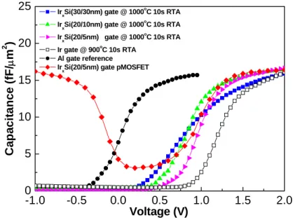
Fig. 2-1 shows the measured C-V characteristics of IrxSi, Ir and Al gates on
HfSiON MOS devices. Low temperature Al gated HfSiON capacitors were used as a
reference because pure metal deposited at low temperature has little interface reaction
with high-κ dielectrics to cause Fermi-level pinning [10]. In addition, the flat band
voltage (Vfb) is expressed as:
Vfb =φms-Qf/Cox = (φm-φs)-(Qf/εokox)tox = (φm-φs)-(Qf/εokSiO2)EOT (1) where φm and φs are the work functions for metal gates and Si, respectively. Qf, Cox,
tox and EOT are the oxide charge, capacitance, physical thickness and
equivalent-oxide thickness for high-κ dielectrics, respectively. Since HfSiON has the
same thermal cycle (1000oC RTA for 10 sec) before Al gate formation, the Q
f effect should be similar to FUSI gates. Therefore, the principal effect of Vfb shift might be
due to the difference of effective φm. In comparing with the conventional φm-eff
extraction from Vfb-tox or Vfb-EOT plot, this method uses a simple process without
fabricating MOS devices with various tox and measuring the thickness carefully by
transmission electron microscopy (TEM). Since the capacitance value or EOT of ~1.6
nm are the same for various gated HfSiON capacitors, the shifts of C-V curves with
different gate electrodes are attributed to the different work functions. Ir/HfSiON after
900oC RTA has a large Vfb shift of 1.15 V to control low temperature Al gates (4.1 eV
close to the reported 5.27 eV for Ir [11], indicating no pinning effect in pure metal Ir
gates. This is due to weak bonding strengths of Ir-O or Ir-N that reduce the
Fermi-level pinning related interface reaction [8]. However, Ir/HfSiON capacitors
failed after 1000oC RTA. To improve thermal stability, additional amorphous Si of
5~30 nm was inserted between Ir and HfSiON. Good C-V characteristics were
measured for IrxSi/HfSiON devices after the required 1000oC RTA for implant
activation, although thermal stability was traded off at the Fermi-level pinning caused
by the Si/HfSiON interface reaction. However, the continuously increasing Vfb toward
the value of pure Ir gates was observed by decreasing the inserted amorphous Si layer,
and a high φm-eff of 4.95 eV was obtained for IrxSi/HfSiON devices with the inserted 5
nm amorphous Si. This 4.95 eV φm-eff is significantly larger than Ni3Si/HfSiON [6].
This result is also slightly better than previous IrxSi/HfAlON [7] due to thinner
amorphous Si on high-κ dielectrics. Slow depletion for IrxSi/HfSiON devices with 30
nm amorphous Si may be due to non-uniform silicidation as examined by TEM,
where locally un-reacted Si was found to cause voltage drop in gate electrodes. The
formation of FUSI gates is evident from the same inversion and accumulation
capacitances measured in MOSFETs.
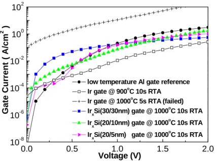
Fig. 2-2 shows the J-V characteristics of IrxSi, Ir and Al gates on high-κ HfSiON
19
sharp contrast, IrxSi gates on HfSiON showed successfully improved thermal stability
to 1000oC RTA, which is evident from low leakage current comparable with P+
poly-Si gates [17]. Here high temperature thermal cycle is required for dopant
activation after ion implantation.
We have further used the X-Ray Diffraction (XRD) measurements to
characterize the IrxSi. As shown in Fig. 2-3, the Ir-rich IrxSi with x=3 was found with
distinct 2θ angle to residual Ir peak. The measured large Vfb shift of IrxSi is supported
by SIMS profile as shown in Fig. 2-4. Here Ir segregation toward amorphous Si was
measured to form IrxSi on HfSiON surface. Such FUSI formation directly on
high-κ dielectrics is known to reduce Fermi-level pinning [6]-[8]. Therefore, good
thermal stability of 1000oCRTA, a reasonable high φm-eff of 4.95 eV, and low gate
dielectric leakage current can be simultaneously achieved in IrxSi/HfSiON MOS
capacitors. To the best of our knowledge, this is the highest reported φm-eff in high-κ
Hf-based oxide [5]-[8]. These are the few methods to achieve a high φm-eff in Hf-based
oxide p-MOS devices. Although the Vfb tuning can be reached by impurity segregation
in FUSI/SiON, this method becomes less useful in high-κ metal-oxide due to the
stronger interface reaction. In the following we will study IrxSi/HfSiON devices with
the thinnest 5 nm amorphous Si. This is because the Vfb of thicker Si layer is too low
Fig. 2-5 shows the transistor Id-Vd characteristics as a function of Vg-Vt for
1000oC RTA Ir
xSi/HfSiON p-MOSFETs. The well-behaved Id-Vd curves of IrxSi/HfSiON transistors show little device performance degradation.
Fig. 2-6 shows the Id-Vg characteristics of IrxSi gated p-MOSFETs with HfSiON
as the gate dielectric. A small Vt as low as -0.15 V is obtained from the linear Id-Vg
plot, which is consistent with the large φm-eff of 4.95 eV from C-V curves and the Ir
accumulation on HfSiON from SIMS.
Figs. 2-7 shows the extracted hole mobilities versus gate electric fields from the
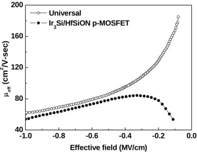
measured Id-Vg data of IrxSi/HfSiON p-MOSFETs. High hole mobilities of 84 and 53
cm2/V-s are obtained at peak value and 1 MV/cm effective field for Ir
xSi/HfSiON p-MOSFETs, respectively, which is compatible with the published data in the
literature [5]-[8]. Good hole mobilities also indicate low Ir diffusion through HfSiON
to inversion channel, even though excess Ir is necessary to prevent un-reacted
amorphous Si from causing gate depletion or increased Fermi-level pinning.
Therefore, a high φm-eff, a small Vt and good hole mobilities are simultaneously
achieved in IrxSi/HfSiONp-MOSFETs with additional merit of process compatible to
current VLSI lines.
2.4 Conclusion
21
φm-eff of 4.95 eV, a small Vt of -0.15 V, a peak hole mobility of 84 cm2/V-s and 1000oC
RTA thermal stability with the advantage of full process compatible to current VLSI
References
[1] J. K. Schaeffer, C. Capasso, L. R. C. Fonseca, S. Samavedam, D. C. Gilmer, Y. Liang, S. Kalpat, B. Adetutu, H.-H. Tseng, Y. Shiho, A. Demkov, R. Hegde, W. J. Taylor, R. Gregory, J. Jiang, E. Luckowski, M. V. Raymond, K. Moore, D. Triyoso, D. Roan, B. E. White Jr, and P. J. Tobin, “Challenges for the integration of metal gate electrodes,” in IEDM Tech. Dig., 2004, pp. 287-290. [2] H.-H. Tseng, C. C. Capasso, J. K. Schaeffer, E. A. Hebert, P. J. Tobin,
D. C. Gilmer, D. Triyoso, M. E. Ramón, S. Kalpat, E. Luckowski, W. J. Taylor, Y. Jeon, O. Adetutu, R. I. Hegde, R. Noble, M. Jahanbani, C. El Chemali, and B. E. White, “Improved short channel device characteristics with stress relieved pre-oxide (SRPO) and a novel tantalum carbon alloy metal gate/HfO2 stack,” in
IEDM Tech. Dig., 2004, pp. 821-824.
[3] B. Tavel, T. Skotnicki, G. Pares, N. Carrière, M. Rivoire, F. Leverd, C. Julien, J. Torres, and R. Pantel, “Totally silicided (CoSi2) polysilicon: a novel approach to very low-resistive gate (~2Ω/ ) without metal CMP nor etching,” in IEDM Tech. Dig., 2001, pp. 815-828.
[4] W. P. Maszara, Z. Krivokapic, P. King, J. S. GooIlgweon, and M. R. Lin, “Transistors with dual work function metal gate by single full silicidation (FUSI) of polysilicon gates,” in IEDM Tech. Dig., 2002, pp.367–370.
[5] T. Nabatame, M. Kadoshima, K. Iwamoto, N. Mise, S. Migita, M. Ohno, H. Ota, N. Yasuda, A. Ogawa, K. Tominaga, H. Satake, and A. Toriumi, “Partial silicides technology for tunable work function electrodes on high-k gate dielectrics- fermi level pinning controlled PtSix for HfOx(N) pMOSFET,” in IEDM Tech.
23
Watanabe, T. Tatsumi, and Y. Mochizuki, “Dual workfunction Ni-silicide/HfSiON gate stacks by phase-controlled full-silicidation (PC-FUSI) technique for 45nm-node LSTP and LOP devices,” in IEDM Tech. Dig., 2004, pp. 91-94.
[7] C. H. Wu, D. S. Yu, A. Chin, S. J. Wang, M.-F. Li, C. Zhu, B. F. Hung, and S. P. McAlister, “High work function IrxSi gates on HfAlON p-MOSFETs,” IEEE
Electron Device Lett. 27, no. 2, pp. 90-92, 2006.
[8] D. S. Yu, A. Chin, C. H. Wu, M.-F. Li, C. Zhu, S. J. Wang, W. J. Yoo, B. F. Hung and S. P. McAlister, “Lanthanide and Ir-based dual metal-gate/HfAlON CMOS with large work-function difference,” in IEDM Tech. Dig., 2005, pp. 649-652. [9] C. H. Huang, D. S. Yu, A. Chin, W. J. Chen, C. X. Zhu, M.-F. Li, B. J. Cho, and
D. L. Kwong, “Fully silicided NiSi and germanided NiGe dual gates on SiO2/Si and Al2O3/Ge-On-Insulator MOSFETs,” in IEDM Tech. Dig., 2003, pp. 319-322. [10] M. Koyama, Y. Kamimuta, T. Ino, A. Kaneko, S. Inumiya, K. Eguchi, M. Takayanagi, and A. Nishiyama, “Careful examination on the asymmetric Vfb shift problem for Poly-Si/HfSiON gate stack and its solution by the Hf concentration control in the dielectric near the Poly-Si interface with small EOT expense,” in IEDM Tech. Dig., 2004, pp. 499-502.
[11] H. B. Michaelson, “The work function of the elements and its periodicity,” J. Appl. Phys., vol. 48, pp. 4729-4733, Nov. 1977.
[12] C. H. Lai, A. Chin, K. C. Chiang, W. J. Yoo, C. F. Cheng, S. P. McAlister, C. C. Chi and P. Wu, “Novel SiO2/AlN/HfAlO/IrO2 memory with fast erase, large ΔVth and good retention,” in Symp. VLSI Tech. Dig., 2005, pp. 210-211.
[13] K. C. Chiang, Albert Chin, C. H. Lai, W. J. Chen, C. F. Cheng, B. F. Hung, C. C. Liao, “Very high k and high density TiTaO MIM capacitors for analog and RF applications,” in Symp. VLSI Tech. Dig., 2005, pp. 62-63.
[14] C. C. Liao, C. F. Cheng, D. S. Yu and A. Chin, “The copper contamination effect on Al2O3 gate dielectric on Si,” J. Electrochem. Soc., vol. 151, pp. G693-G696, Oct. 2004.
[15] Y. H. Lin, F. M. Pan, Y. C. Liao, Y. C. Chen, I. J. Hsieh, and A. Chin, “The Cu contamination effect in oxynitride gate dielectrics,” J. Electrochem. Soc., vol. 148, G627-G629, Nov. 2001.
[16] Y. T. Hou, F.Y. Yen, P. F. Hsu, V. S. Chang, P. S. Lim, C. L. Hung, L. G. Yao, J. C. Jiang, H. J. Lin, Y. Jin, S. M. Jang, H. J. Tao, S. C. Chen and M. S. Liang, “High performance tantalum carbide metal gate stacks for nMOSFET Application,” in IEDM Tech. Dig., 2005, pp. 35-39.
[17] A. L. P. Rotondaro, M.R. Visokay, J.J. Chambers, A. Shanware, R. Khamankar, H. Bu, R.T. Laaksonen, L. Tsung, M. Douglas, R. Kuan, M.J. Bevan, T. Grider, J. Mcpherson, and L. Colombo, “Advanced CMOS transistors with a novel HfSiON gate dielectric,” in Symp. VLSI Tech. Dig., 2002, pp. 148-149.
25 -1.0 -0.5 0.0 0.5 1.0 1.5 2.0 0 5 10 15 20 25 Ir xSi(30/30nm) gate @ 1000 oC 10s RTA Ir xSi(20/10nm) gate @ 1000 oC 10s RTA Ir xSi(20/5nm) gate @ 1000 oC 10s RTA Ir gate @ 900oC 10s RTA Al gate reference Ir
xSi(20/5nm) gate pMOSFET
Voltage (V) Ca pa cit a nc e (fF/ μ m 2 )
Fig. 2-1 C-V characteristics of HfSiON/n-Si with Ir
xSi, Ir and Al gates
0.0 0.5 1.0 1.5 2.0 10-8 10-6 10-4 10-2 100 102 G a te C u rrent ( A/cm 2 ) Voltage (V)
low temperature Al gate reference Ir gate @ 900oC 10s RTA
Ir gate @ 1000oC 5s RTA (failed) IrxSi(30/30nm) gate @ 1000oC 10s RTA IrxSi(20/10nm) gate @ 1000oC 10s RTA IrxSi(20/5nm) gate @ 1000oC 10s RTA
Fig. 2-2 J-V characteristics of HfSiON/n-Si with Ir
xSi, Ir and Al gates
27 20 30 40 50 60 unreacted Ir Int ensi ty
(
cp s)
2θ (Degree) Ir xSi @ 1000oC RTAIr/Si @ Room Temp.
Ir3Si (202)
0 50 100 150 200 103
104 105 106
accumulation toward HfSiON
Si (1000oC RTA) Si (950oC RTA) Si (900oC RTA) Ir (1000oC RTA) Ir (950oC RTA) Ir (900oC RTA)
Sputter Time (sec)
In te n s ity ( c o u n ts ) Ir3Si Ir Ir accumulation HfSiON
Fig. 2-4 SIMS profile of Ir
3Si gates on HfSiON at different RTA
temperature. The Ir
3Si accumulated toward HfSiON interface is
29 -2.5 -2.0 -1.5 -1.0 -0.5 0.0 0.0 0.5 1.0 1.5 2.0 2.5 3.0 3.5 4.0 I d (m A ) Vd (V) |Vg-VT|=0 V |Vg-VT|=0.5 V |Vg-VT|=1 V |Vg-VT|=1.5 V Ir3Si/HfSiON p-MOSFET W/L = 200 μm/10 μm
-2.0 -1.5 -1.0 -0.5 0.0 0.5 10-10 10-9 10-8 10-7 10-6 10-5 10-4 10-3 Id (A) Vg (V) Ir3Si/HfSiON p-MOSFET Vds = -0.1 V W/L = 200 μm/10 μm
31 -1.0 -0.8 -0.6 -0.4 -0.2 0.0 40 80 120 160 200 Universal Ir 3Si/HfSiON p-MOSFET μ eff ( cm 2 /V-sec ) Effective field (MV/cm)
Fig. 2-7 The extracted hole mobilities from I
d-V
gcharacteristics of
Ir
3Si/HfSiON p-MOSFETs.
Chapter 3
HfSiON n-MOSFETs Using Low Work Function
HfSi
xGates
3.1 Introduction
To continue the VLSI scaling trend, the using metal gate and high-κ gate
dielectric are needed to reduce the DC power consumption and gate depletion [1]-[12].
However, one of the difficult challenges for metal-gate/high-κ MOSFET is the large
threshold voltage (Vt) by Fermi-level pinning that is opposite to scaling trend. To
overcome this problem, low and high work-function metal-gates are required to
reduce the pinning effect. Previously, we have reported the IrxSi gate on HfAlON has
high effective work-function (φm-eff) of 4.9 eV [12] and useful for p-MOS. For
n-MOSFET, the novel TaC gate has shown low φm-eff [1]-[2]. However, the Full
Silicidation (FUSI) gate [3]-[5], [8]-[13] for n-MOS is still needed to develop, which
is due to the inherent advantage of the process compatibility with current poly-Si gate
CMOS technology. In this chapter, we have used the similar method of previously
reported IrxSi for p-MOS [12] to develop the low work-function HfSix gate for
n-MOSFET. This is because the Hf has very low work function of 3.5 eV in the
33
amorphous-Si, gives a low φm-eff of 4.27 eV and a good electron mobility of 216
cm2/V-s. In addition, the HfSi
x/HfSiON can sustain a high RTA temperature annealing of 1000oC that is compatible with current VLSI process line. These results
indicate the potential application for metal-gate/high-κ n-MOSFETs.
3.2 Experimental procedure
We have used the 12-inch p-type Si wafers in this study. After standard clean, the
HfSiO was deposited by atomic-layer deposition (ALD) and the HfSiON was formed
by applying direct nitrogen plasma to HfSiO surface. Then amorphous Si with various
thickness of 50 to 5 nm was deposited on HfSiON as a silicide layer and metal barrier
for subsequently deposited Hf by PVD. A Mo layer was also deposited to cover the Hf
to prevent oxidation. The MOS capacitor was formed by patterning and RTA
annealing at 1000oC for 10 sec. For n-MOSFET, additional 150 nm thick
amorphous-Si was deposited on Hf/Si/HfSiON to prevent ion implantation
penetration through gate, where the n+ source-drain regions are formed by using a
phosphorus ion implantation at 35 KeV. Then the 1000oC RTA was applied to activate
the implanted dopant and the n-MOSFET was fabricated by this self-aligned gate first
process. Note that the FUSI HfSix gate is formed at high temperature RTA and similar
to previous IrxSi gate [12], which are different from conventional low temperature
to the Si/HfSiON interface may also reduce the reaction of thin amorphous Si (5 nm)
with high-κ dielectric to cause Fermi-level pinning. For comparison, Al gated devices
on HfSiON were also formed. The fabricated devices were characterized by C-V and
I-V measurements.
3.3 Results and discussion
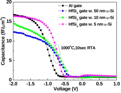
Figs. 3-1 shows the C-V characteristics for HfSix/HfSiON and control
Al/HfSiON capacitors, where the HfSix gate was formed at 1000oC RTA. The
Al-gated capacitor was used as a reference since it is known to have little Fermi-level
pinning of low-temperature deposited pure metal gate on high-κ dielectric [7]. For
thicker amorphous-Si of 50 and 10 nm on HfSiON, the capacitance density decreases
with increasing the thickness of amorphous-Si indicating in HfSix gate on HfSiON not
fully silicided. This in tern gives a higher flat band voltage (Vfb) due to the Fermi-level
pinning on high-κ dielectric. In contrast, the HfSix formed by thin 5 nm amorphous-Si
shows the same capacitance density with control Al gate suggesting the successful
FUSI gate formation. From the C-V shift referenced to the control Al gate, an
extracted φm-eff of 4.27 eV is obtained for HfSix/HfSiON that is suitable for n-MOS
application. The low Vfb and φm-eff for HfSix gate capacitors with 5 nm amorphous-Si
may be due to the Hf diffusion toward the HfSiON surface through thin amorphous-Si
35
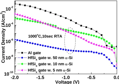
HfSix/HfSiON and control Al/HfSiON capacitors. Low leakage current of 1.9×10⁻⁵
A/cm at -1 V is measured at an equivalent oxide thickness (EOT) of ~1.6 nm, which
suggests the good thermal stability of HfSix gate on HfSiON dielectric even after
1000oC RTA. Therefore, improved Fermi-level pinning, reasonable low φm-eff of 4.27
eV and a low gate dielectric leakage current can be achieved in HfSix/HfSiON MOS
capacitors at the same time.
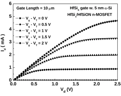
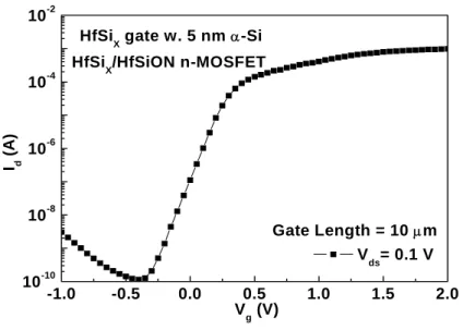
Fig. 3-3 shows the transistor Id-Vd characteristics as a function of Vg-Vt for the
1000oC RTA-annealed HfSi
x/HfSiON n-MOSFETs. The well-behaved Id-Vd curves indicate the good device performance by using an HfSix gate. Fig. 3-4 displays Id-Vg
characteristics of the HfSix/HfSiON n-MOSFETs. A low Vt of only 0.1 V was
measured from the linear Id-Vg plot, which is due to the low φm-eff of 4.27 eV from the
C-V measurements.
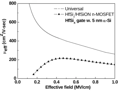
Fig. 3-5 shows the electron mobility extracted from the measured Id-Vg curves
of the n-MOSFETs. A peak electron mobility of 216 cm2/V-s was obtained for the
HfSix/HfSiON n-MOSFETs, which is close to published data in literature [13]-[14].
3.4 Conclusion
Using the novel HfSix gate formed by thin amorphous-Si on HfSiON, good
device performance has been obtained for n-MOSFETs with low φm-eff and Vt values.
37
References
[1] J. K. Schaeffer, C. Capasso, L. R. C. Fonseca, S. Samavedam, D. C. Gilmer, Y. Liang, S. Kalpat, B. Adetutu, H.-H. Tseng, Y. Shiho, A. Demkov, R. Hegde, W. J. Taylor, R. Gregory, J. Jiang, E. Luckowski, M. V. Raymond, K. Moore, D. Triyoso, D. Roan, B. E. White Jr, and P. J. Tobin, “Challenges for the integration of metal gate electrodes,” in IEDM Tech. Dig., 2004, pp. 287-290. [2] H.-H. Tseng, C. C. Capasso, J. K. Schaeffer, E. A. Hebert, P. J. Tobin,
D. C. Gilmer, D. Triyoso, M. E. Ramón, S. Kalpat, E. Luckowski, W. J. Taylor, Y. Jeon, O. Adetutu, R. I. Hegde, R. Noble, M. Jahanbani, C. El Chemali, and B. E. White, “Improved short channel device characteristics with stress relieved pre-oxide (SRPO) and a novel tantalum carbon alloy metal gate/HfO2 stack,” in
IEDM Tech. Dig., 2004, pp. 821-824.
[3] B. Tavel, T. Skotnicki, G. Pares, N. Carrière, M. Rivoire, F. Leverd, C. Julien, J. Torres, and R. Pantel, “Totally silicided (CoSi2) polysilicon: a novel approach to very low-resistive gate (~2Ω/ ) without metal CMP nor etching,” in IEDM Tech. Dig., 2001, pp. 815-828.
[4] W. P. Maszara, Z. Krivokapic, P. King, J. S. GooIlgweon, and M. R. Lin, “Transistors with dual work function metal gate by single full silicidation (FUSI) of polysilicon gates,” in IEDM Tech. Dig., 2002, pp.367–370.
[5] T. Nabatame, M. Kadoshima, K. Iwamoto, N. Mise, S. Migita, M. Ohno, H. Ota, N. Yasuda, A. Ogawa, K. Tominaga, H. Satake, and A. Toriumi, “Partial silicides technology for tunable work function electrodes on high-k gate dielectrics- fermi level pinning controlled PtSix for HfOx(N) pMOSFET,” in IEDM Tech. Dig., 2004, pp.83-86.
[6] C. S. Park, B. J. Cho, L. J. Tang, and D. L. Kwong, “Substituted aluminum metal gate on high-K dielectric for low work-function and Fermi-level pinning free,” in IEDM Tech. Dig., 2004, pp. 299 - 302.
[7] M. Koyama, Y. Kamimuta, T. Ino, A. Kaneko, S. Inumiya, K. Eguchi, M. Takayanagi, and A. Nishiyama, “Careful examination on the asymmetric Vfb shift problem for Poly-Si/HfSiON gate stack and its solution by the Hf concentration control in the dielectric near the Poly-Si interface with small EOT expense,” in IEDM Tech. Dig., 2004, pp. 499-502.
[8] K. Takahashi, K. Manabe, T. Ikarashi, N. Ikarashi, T. Hase, T. Yoshihara, H. Watanabe, T. Tatsumi, and Y. Mochizuki, “Dual workfunction Ni-silicide/HfSiON gate stacks by phase-controlled full-silicidation (PC-FUSI) technique for 45nm-node LSTP and LOP devices,” in IEDM Tech. Dig., 2004, pp. 91-94.
[9] C. H. Huang, D. S. Yu, A. Chin, W. J. Chen, C. X. Zhu, M.-F. Li, B. J. Cho, and D. L. Kwong, “Fully Silicided NiSi and germanided NiGe dual gates on SiO2/Si and Al2O3/Ge-On-Insulator MOSFETs,” in IEDM Tech. Dig., 2003, pp. 319-322. [10] C. Y. Lin, D. S. Yu, A. Chin, C. Zhu, M. F. Li, and D. L. Kwong, “Fully silicided
NiSi gate on La2O3 MOSFETs,” IEEE Electron Device Lett. 24, pp. 348-350, May 2003.
[11] D. S. Yu, K. C. Chiang, C. F. Cheng, A. Chin, C. Zhu, M. F. Li, and D. L. Kwong, “Fully Silicided NiSi:Hf/LaAlO3/Smart-Cut-Ge-On-Insulator n-MOSFETs with high electron mobility” IEEE Electron Device Lett. 25, pp. 559-561, Aug. 2004. [12] C. H. Wu, D. S. Yu, Albert Chin, S. J. Wang, M.-F. Li, C. Zhu, B. F. Hung, and S.
P. McAlister, “High work function IrxSi gates on HfAlON p-MOSFETs,” IEEE
39
[13] A. Veloso, K. G. Anil, L. Witters, S. Brus, S. Kubicek, J.-F. de Marneffe, B. Sijmus, K. Devriendt, A. Lauwers, T. Kauerauf, M. Jurczak, and S. Biesemans, “Work function engineering by FUSI and its impact on the performance and reliability of oxynitride and Hf-silicate based MOSFETs,” in IEDM Tech. Dig., pp. 855-858, 2004.
[14] S. J. Rhee, C. S. Kang, C. H. Choi, C. Y. Kang, S. Krishnan, M. Zhang, M. S. Akbar, and J. C. Lee, “Improved electrical and material characteristics of hafnium titanate multi-metal oxide n-MOSFETs with ultra-thin EOT (~8Å) gate dielectric application,” in IEDM Tech. Dig., pp.837-840, 2004.
-2.0 -1.5 -1.0 -0.5 0.0 0.5 1.0 0 5 10 15 20 Al gate HfSi X gate w. 50 nm α-Si HfSi X gate w. 10 nm α-Si
HfSiX gate w. 5 nm α-Si
Cap acita nce (fF/ μ m 2 ) Voltage (V) 1000oC,10sec RTA
Fig. 3-1 C-V characteristics for high temperature RTA formed
HfSi
x/HfSiON and low temperature Al/HfSiON capacitors. The
41 -2.0 -1.5 -1.0 -0.5 0.0 10-10 10-8 10-6 10-4 10-2 Al gate
HfSiX gate w. 50 nm α-Si HfSiX gate w. 10 nm α-Si HfSiX gate w. 5 nm α-Si
Voltage (V)
Current Density
(A/cm
2 )
1000oC,10sec RTA
Fig. 3-2 J-V characteristics of HfSi
x/HfSiON and low temperature
0.0 0.5 1.0 1.5 2.0 2.5 0 1 2 3 4 5 6
HfSiX gate w. 5 nm α-Si HfSix/HfSiON n-MOSFET Gate Length = 10 μm I d ( mA ) Vd (V) Vg - VT = 0 V Vg - VT = 0.5 V Vg - VT = 1 V Vg - VT = 1.5 V Vg - VT = 2 V
Fig. 3-3 The I
d-V
dcharacteristics of HfSi
x/HfSiON n-MOSFETs. The
43 -1.0 -0.5 0.0 0.5 1.0 1.5 2.0 10-10 10-8 10-6 10-4 10-2
HfSiX gate w. 5 nm α-Si
Gate Length = 10 μm
HfSiX/HfSiON n-MOSFET
I d
(A)
Vg (V)
Vds= 0.1 V
Fig. 3-4 The I
d-V
gcharacteristics HfSi
x/HfSiON n-MOSFETs. The
0.0 0.2 0.4 0.6 0.8 1.0 0 200 400 600 800
HfSiX gate w. 5 nm α-Si
Universal
HfSix/HfSiON n-MOSFET
Effective field (MV/cm) μef f (cm 2 /V-se c )
45
Chapter 4
Novel High-
κ HfLaON n-MOSFETs with Preserved
Amorphous State to 1000
oC
4.1 Introduction
The high-κ gate dielectric is needed for future generation MOSFET to reduce the
dc power consumption [1]-[16]. The ideal high-κ MOSFET requires higher κ value
for lower leakage current, less Fermi-level pinning for low threshold voltage (Vt),
high mobility and 1000oC stability for ion implant doping activation. Unfortunately,
the widely studied HfO2 [1]-[2] is known to react with Si substrate at high temperature
and causes κ value reduction. The other problem of HfO2 is the unwanted
crystallization at high temperature- this is different from the currently used
amorphous SiO2 or SiON and may cause charge trapping in poly-grain boundaries. To
overcome these problems, the HfSiON [3]-[6] and HfAlON [7] are developed by
adding high temperature stable SiO2, Al2O3 and Nitrogen into HfO2. However, again
the κ value is reduced. An alternative way is to increase the dielectric entropy, which
is realized by adding another high-κ such as Ta2O5 into HfO2 [8]. Nevertheless, the
small conduction band discontinuity of ~0.3 eV for Ta2O5/Si is the major concern. To
[9]-[11] with less Fermi-level pinning by added La2O3 [12]-[16]. However, the
crystallization temperature of HfLaO is close to 900oC [9], [11] but still less than the
required 1000oC RTA for source-drain implant activation. In this chapter, we have
developed the novel HfLaON gate dielectric that remains amorphous at 1000oC with
still high-κ value of 20. After a 1000oC RTA, the self-aligned TaN/HfLaON MOSFET
showed low leakage current of 2.7×10⁻⁶ A/cm2 at 1 V above flat-band voltage (Vfb), an
effective work function (φm-eff) of 4.24eV and a peak electron mobility 217 cm2/V-s at
1.6 nm equivalent-oxide thickness (EOT), with additional merit of full process
compatible with current VLSI fabrication lines.
4.2 Experimental procedure
After standard clean, the 7 nm thick HfLaO with 1 to 1 Hf:La ratio was deposited
by physical vapor deposition (PVD) and followed by post deposition anneal (PDA),
although atomic layer deposition (ALD) of HfO2 and La2O3 [15] were previously
demonstrated. The HfLaON was formed by applying NH3 plasma surface nitridation
[6]-[7] on HfLaO. The gate-first TaN/HfLaON n-MOSFET was fabricated by
depositing 150 nm TaN by PVD, device patterning, phosphorus ion implantation to
source-drain at 25 KeV and 5×1015 cm-2 dose, and 1000oC RTA to activate the
implanted dopant. This self-aligned process is fully compatible with currently used
47
examined by grazing incident x-ray diffraction (XRD), X-ray Photoelectron
Spectroscopy (XPS), Transmission Electron Microscope (TEM) and Secondary Ion
Mass Spectrometry (SIMS) measurements and the fabricated n-MOSFETs were
characterized by C-V and I-V measurements.
4.3 Results and discussion
Fig. 4-1 shows the XRD spectra of HfLaO under different RTA temperature.
Although the HfLaO is amorphous at 800oC RTA, strong unwanted crystallization is
clearly measured at 1000oC RTA for 10 sec. This result is consistent with previous
study on HfLaO crystallization [9], [11]. The XRD spectra of HfLaON under different
RTA temperature are shown in fig. 4-2. In sharp contrast, the HfLaON can remain the
amorphous state even after the same 1000oC for 10 sec RTA.
The existence of Hf, La, O and N in HfLaON is confirmed by XPS in Fig. 4-3.
The dielectric physical interface was further examined by cross-sectional TEM in Fig.
4-4. The TEM photo shows good amorphous HfLaON even after 1000oC RTA and
smooth interface.
Fig. 4-5 & 4-6 show the J-V and C-V characteristics on various nitridation
conditions for HfLaON: the thermal stability at 1000oC RTA improves with increasing
NH3+ time but trading off the increasing pinning effect compared with previous
Figs. 4-7 and 4-8 show the C-V and J-V characteristics for TaN/HfLaON MOS
capacitors with various RTA temperatures, respectively. Low Vfb away from midgap is
still measured even after 1000oC RTA. A φm-eff of 4.24 eV is obtained by the Vfb shift
to control Al gate on 1000oC-annealed HfLaON. Such low temperature deposited
metal gate is known to have little interface reaction caused Fermi-level pinning [3],
[6]-[7] and the same 1000oC RTA thermal cycle ensures the close oxide charges.
Although the φm-eff is relatively higher than the TaN/HfLaO [10]-[11] by surface
nitridation in HfLaON, this is traded off the 1000oC amorphous state stability. In
addition, low leakage current of 2.7×10⁻⁶ A/cm2 was obtained at 1 V above Vfb with
1.6 nm EOT. From the careful thickness measurement from cross-sectional
transmission electron microscopy, a κ value of 20 is still obtained even after 1000oC
RTA that is in sharp contrast to the degraded κ in HfO2 by interfacial silicate
formation [9]. Therefore, low gate dielectric leakage current, low φm-eff and improved
1000oC amorphous state stability are simultaneously obtained in novel HfLaON MOS
capacitors using simple TaN gate.
The TaN/HfLaON structures are further analyzed by SIMS. Fig. 4-9 shows the
SIMS profile of TaN gate on HfLaON at different RTA temperature. No Ta
49
to the nitridation on thick high-κ that prevents TaN metal from diffusing through the
HfLaON gate dielectric.
Fig. 4-10 shows the comparison of gate leakage current density for MOS devices
with SiO2 and HfLaON gate dielectric. Much improved leakage current than SiO2 is
obtained at 1.6 nm EOT. The dielectric constant of HfLaON at different RTA
temperature is shown in fig. 4-11. Significant higher κ value of 20 is still preserved
even after 1000oC RTA and much better than HfO 2.
Fig. 4-12 shows the transistor Id-Vd characteristics of the 1000oC RTA-annealed
TaN/HfLaON n-MOSFETs. The well-behaved Id-Vd curves indicate the good device
performance by using a TaNgate. Furthermore, a low Vt of 0.18 V was measured from
the linear Id-Vg characteristics shown in fig. 4-13, which is due to the low φm-eff from
the C-V measurements.
Fig. 4-14 shows the electron mobility extracted from the measured Id-Vg
characteristics of the n-MOSFETs. A peak electron mobility of 217 cm2/V-s was
obtained for the TaN/HfLaON n-MOSFETs, which is close to the published data of
Hf-based oxides in literature [2]-[3], [5]-[8].
Further reliability study is from the BTI shown in fig. 4-15. The threshold
voltage shifts (ΔVt) < 20 mV are measured for TaN/HfLaON n-MOSFETs at 10
4.4 Conclusion
We have developed novel high-κ HfLaON gate dielectric that can preserve the
amorphous state to 1000oC RTA and similar with currently used SiO
2 or SiON. The gate-first and self-aligned TaN/HfLaON n-MOSFETs showed low leakage current of
2.7×10⁻⁶ A/cm2 at 1 V above flat-band voltage, an effective work function of 4.24 eV
and a peak electron mobility 217 cm2/V-s at 1.6 nm equivalent-oxide thickness, with