國
立
交
通
大
學
電機學院微電子奈米科技產業研發碩士班
碩 士 論 文
低臨限電壓與高驅動電流之薄膜電晶體在金屬鋁與介電層氧
化鑭鉿上之研究
Low Threshold Voltage and High Drive Current Poly-Silicon Thin Film
Transistors Using Aluminum Metal Gate and HfLaO Dielectric
研 究 生:黃群懿
指導教授:荊鳳德 教授
低臨限電壓與高驅動電流之薄膜電晶體在金屬鋁與介電層氧
化鑭鉿上之研究
Low Threshold Voltage and High Drive Current Poly-Silicon Thin Film
Transistors Using Aluminum Metal Gate and HfLaO Dielectric
研 究 生:黃群懿 Student:Chen-Yi Huang
指導教授:荊鳳德 Advisor:Dr. Albert Chin
國 立 交 通 大 學
電機學院微電子奈米科技產業研發碩士班
碩 士 論 文
A Thesis
Submitted to College of Electrical and Computer Engineering National Chiao Tung University
in partial Fulfillment of the Requirements for the Degree of
Master in
Industrial Technology R & D Master Program on Microelectronics and Nano Sciences
January 2008
低臨限電壓與高驅動電流之薄膜電晶體在金屬鋁與
介電層氧化鑭鉿上之研究
研究生: 黃群懿 指導教授: 荊鳳德 教授
國立交通大學電機學院產業研發碩士班
摘要
本論文將高介電常數的氧化鑭鉿整合至低溫多晶矽薄膜電晶體當作 閘極氧化層,並且選用鋁來作為金屬閘極在LTPS 上。將可得到高驅動電流、 低臨界電壓和低次臨界斜率,大大提升了元件的特性。不僅如此,也因此而達 成高的開/關電流比例及閘極崩潰電場。上述所得之優秀的特性與所使用的閘極 氧化層種類有密切關係。 使用氧化鑭鉿作為閘極氧化層,可造成高閘極電容密度與很小的等效 氧化層厚度。有別於一般的TFT 元件,此種元件並不需使用一些介面鈍化處理 或是特別的結晶步驟,只需要用爐管就可以達到成晶的目的了。Low Threshold Voltage and High Drive Current
Poly-Silicon Thin Film Transistors Using Aluminum Metal
Gate and HfLaO Dielectric
Student: Chen-Yi Huang Advisor: Dr. Albert Chin
Industrial Technology R & D Master Program of
Electrical and Computer Engineering College
National Chiao Tung University
Abstract
We have integrated a Metal gate into Low temperature Poly-Silicon(LTPS) thin-film transistors (TFTs) with high- κ gate dielectric. We used Aluminum for metal gate, and we used HfLaO for high-κ gate dielectric on LTPS. We got high drive current, low threshold voltage and low sub-threshold slop to improve the performance of device obviously. It also achieved high on/off ratio and high gate breakdown electric field. The excellent performances mentioned above are related closely to gate dielectric.
We used HfLaO for high-κ dielectric and it can product high density gate capacitor and less EOT. This kind of device is different from other common devices because it is not necessary to apply passive treatment or specific process of crystallization. We only used furnace to crystallize.
誌 謝
感謝我的恩師荊鳳德教授在這兩年的碩士訓練期間,給予我許多的鼓 勵,尤其是在情緒低落的時候,適時的聽到老師鼓勵的話,例如:Perfect、 Excellent…….等鼓勵的話語,雖然自己知道有時候並不如老師所鼓勵的那樣 好,但是老師的鼓勵的確也給實驗室許多士氣提升,最重要的是觸發我們對新 事物的好奇,而想要去研究它、突破它。 其次,要感謝實驗室的學長們。首先要感謝帶我做實驗的蘇迺超學 長、吳建宏學長,從一開始機台的學習,到後來的對實驗的研究與分析,都讓 我學習到非常寶貴的經驗,尤其難忘的是跟學長在深夜裡,一起在奈米中心與 NDL 做實驗,讓我真正的體會到學長對於實驗的熱忱與用心,再此也祝福迺超 學長能夠順利的獲得博士學位。此外存甫學長、淳護學長、明峰學長、立鳴學 長,感謝你們對我的教導與鼓勵。 再來,我要感謝我實驗室的同學,俊賢、建弦、佩諭、哲偉、俊哲、 冠霖、思麟、維邦、坤億、富國、膺任,因為有你們,實驗室才有生氣勃勃的 氣息,也才有許許多多的資源可以共享。 最後我要感謝我所信仰的上帝,讓我在這麼好的環境中學習,也讓我 在許多的人生交叉口中,給予我指引,也賜給我這麼美好的家人,讓我可以無 後顧之憂來完成學業。感謝交大給我這麼棒、這麼精緻的校園,藏書豐富的浩 然圖書館,設備健全的體育館,全國數一數二的實驗儀器,真的、只有讀過交 大才能夠真正的感受到它的好。Contents
Chinese Abstract
………..……..………iEnglish Abstract
……….………...iiAcknowledgement
……….………..iiiContents
……….……….………....ivChapter 1: Introduction
1.1Overview of Polycrystalline Silicon Thin-Film Transistors Technology…1 1.2 Overview of high-k gate dielectrics……….……….….31.3 Motivation………7
1.4 Thesis Outline………...8
Chapter 2: Basic Device Physics
2.1 Energy band in silicon………102.2 n-type and p-type silcon………..10
2.3 Energy-band diagram of an MOS system……….12
2.4.1 Flat band and accumulation………13
2.4.2 Depletion and Inversion………...14
2.5 MOSFET Devices………15
2.6 Thin Film Transitor Devices………...16
2.7 Poly-Silicon Recrystallization……….17
2.7.1 Solid-Phase Crystallization Process Technology………...17
2.7.2 Metal-Induce Lateral Crystallization Process Technology………..18
2.7.3 Rapid Thermal Annealing Crystallization Process Technology………..19
2.7.4 Excimer Laser Annealing Crystallization Process Technology………...20
Chapter 3: The experimental steps and Device Characterization
3.1 Device Fabrication Process………29
3.2 Measurement Tools ………30
3.3 Parameter Extraction………..30
3.3.1 Determination of Threshold Voltage………..30
3.3.2 Determination of Field Effect Mobility………...32
3.3.3 Determination of Sub-threshold Slope………33
3.3.4 Determination of ON/OFF Current Ratio………..33
Chapter 4: Result & Discussion
4.1 Experimental Data Result & Discussion………46Chapter 5: Conclusion
………66Chapter 6 : Reference
……….67Chapter 1
Introduction
1.1 Overview of Polycrystalline Silicon Thin-Film
Transistors Technology
The thin film transistors (TFTs) are widely used in a flat-panel display, in which light must be able to pass through the substrate material to reach the viewer. A Silicon wafer is opaque and obviously will not allow light to transmit through it. Glass is the most commonly used starting substrate because it is highly transparent and is compatible with conventional semiconductor processing steps. Since glass is not a semiconductor like silicon, a thin film of silicon is deposited on top and the transistors are fabricated using this thin layer. Hence, we call “thin-film transistor.”
The thin film transistor technology is similar to the conventional metal oxide semiconductor field effect transistor (MOSFET). Both of them are contain layers of semiconductor, dielectric, and conductive thin films, and are fabricated with semiconductor process. However, there are still some differences between these two devices. In the MOSFETs, the channel region is formed in the single crystal silicon wafer. Several high-temperature process steps, such as oxide growth, dopant annealing, and epitaxy growth, are involved in the the fabrication of MOSFETs. The bulk film and film-film interface
properties are stabilized and determined by the highest process temperature. In contrast to MOSFETs, all thin film layers of TFTs are deposited including the active region. With the glass whose melting temperature is lower than 600oC, all thin film deposition process need to be executed in low temperature.
The most significant advantages of amorphous silicon TFTs are their low-cost and low temperature process technologies. The low-temperature process allows circuits to be fabricated on low-cost and large size glass substrates. However, the low current-driving capability of a-Si TFTs limits their applications to low-gain and low-speed circuits. Therefore, the interest in polycrystalline silicon thin film transistor technology has increased extensively in recent years.
Traditionally, AMLCDs were fabricated using hydrogentated amorphous silicon (a-Si:H)TFTs for the pixel switching devices. The a-Si:H TFTs have many advantages, particularly its compatibility with low temperature process on large glass substrate and high off-state resistivity which result a low leakage current. However, the low electron field effect mobility in a-Si:H TFTs has limited the technology development for AMLCDs application. To integrate the switching elements with the driving circuits on the same substrate is very desirable not only to reduce the cost but also to improve the system performance. Therefore, poly-Si TFTs, which provide higher electron field effect mobility, have been developed as a
lower photocurrent, CMOS capability and better reliability, thus enables the integration of peripheral circuits as well as the active-matrix switching elements on the same substrate.
It should be noted that “poly-Si” covers a range of thin film materials, which vary in the methods of preparation, grain size and nature, distribution of intragranular and bulk defects, and surface roughness. Thus, the properties of any particular film will be dependent on these parameters, which have therefore been the subject of extensive studies to optimize key TFTs parameters such as off-current, on-current, subthreshold swing and mobility. The performance of poly-Si TFTs is strongly influenced by grain boundaries and intragranular defects. In order to enhance TFTs electrical characteristics, several techniques which are used to increase the grain sizes of poly-Si films have been proposed. The methods for recrystallization of a-Si to poly-Si at glass-compatible temperatures are the key technology for fabricating low-temperature process (LTP) poly-Si TFTs on glass. It was reported that the a-Si film can be recrystallized by several techniques, such as: solid-phase crystallization (SPC), excimer laser annealing (ELA), metal-induce lateral crystallization (MILC), and rapid thermal annealing (RTA) to obtain larger grain sizes of poly-Si for high mobility.
1.2 Overview of high-κ gate dielectrics
for SiO2 as the gate dielectric material for sub-0.1 mm complementary
metal–oxide–semiconductor (CMOS) technology. A systematic consideration of the required properties of gate dielectrics indicates that the key guidelines for selecting an alternative gate dielectric are (a) permittivity (b) band-gap (c) band alignment to silicon (d) thermodynamic stability (e) film morphology (f) interface quality (g) compatibility with the current or expected materials to be used in processing for CMOS devices (h) process compatibility (i) reliability [1]-[6]. Many dielectrics appear favorable in some of these areas, but very few materials are promising with respect to all of these guidelines. Specifically, a dielectric constant (κ)~25 is required to satisfy the requirements for CMOS gate dielectrics leading out to years beyond 2010. Similar or larger values are required for dielectrics used in embedded dynamic random access memory (DRAM) cells and radiofrequency (RF) coupling capacitors. The material must also respond positively to a series of other demands relating to such effects as lack of interactivity with the Si substrate, low leakage currents, low interface state density, high electrical barriers against charge injection, etc. The gate leakage current through the gate oxide increases significantly because direct tunneling is the primary conduction mechanism in down-scaling CMOS technologies. Therefore, the engineering of high-κ gate dielectrics have attracted great attention and played an important role in VLSI technology.
In the case of increasing the gate capacitance, consider a parallel plate capacitor (ignoring quantum mechanical and depletion effects from a Si substrate and gate):
t
A
k
C
=
∈
0(1)
Where κ is the dielectric constant (also referred to as the relative permittivity in this article) of the material, 0 is the permittivity of free space (= 8.85×10⁻³ fF/µm), A is the area of the
capacitor, and t is the thickness of the dielectric. This expression for C can be rewritten in terms of teq (i.e., equivalent oxide thickness) and κox (=3.9, dielectric constant of SiO2) of the
capacitor. The term teq represents the theoretical thickness of SiO2 that would be required to
achieve the same capacitance density as the dielectric (ignoring issues such as leakage current and reliability). For example, if the capacitor dielectric is SiO2, teq = 3.9 0 (A/C), and a
capacitance density of C/A = 34.5 fF/µm2 corresponds to teq = 10 Å. Thus, the physical
thickness of an alternative dielectric employed to achieve the equivalent capacitance density of teq = 10 Å can be obtained from the expression
k high k high ox eq
k
t
k
t
− −=
(2a) or simply, eq k high eq ox k high k hight
k
t
k
k
t
9
.
3
− − −=
=
(2b)A dielectric with a relative permittivity of 16 therefore affords a physical thickness of ~40 Å to obtain teq = 10 Å. (As noted above, actual performance of a CMOS gate stack
does not scale directly with the dielectric due to possible quantum mechanical and depletion effects.)
According to the ITRS (International Technology Roadmap for Semiconductor)[7], the suitable gate dielectrics must have κ value more than 8 for 50-70 nm technology nodes and that must be more than 15 when the technology dimension less than 50 nm.
Research on finding an appropriate substitute to the superior SiO2 has been going
on for almost a decade. Oxy-nitrides (SiOxNy) have been introduced to extend the use of SiO2 in production but eventually it has to be replaced by a high-κ material, such as Ta2O5,
TiO2, HfO2, ZrO2, Al2O3, La2O3 or mixtures of them or metal-oxide-silicates of the mentioned
compounds. However, most metal oxides will have the characteristics of crystallization at elevated temperature which cause devices generate non-uniform leakage distribution and give large statistical variation for nano-meter devices across the chip. Therefore, replacement gate strategies have been proposed to prevent crystallization and deleterious effects of mass and electrical transport along grain boundaries.
1.3 Motivation
The dimension of poly-Si TFTs needs to be scaled down to increase the aperture ratio in TFTs array and also the driving speed in peripheral circuits. However, small dimensional effects including short channel effects and narrow width effect influence device characteristics seriously. Good control of device performance isessential for the realization of applying these small dimension poly-Si TFTs. Compared to MOSFETs and SOIs, only a few studies had focused on the small dimension poly-Si TFTs. Whereas the behaviors of short channel poly-Si TFTs are even more complicated than MOSFETs and SOIs due to the poly-Si channel film. Moreover, due to the presence of abundant grain boundary trap states, n-channel poly-Si TFTs are found to exhibit more severe impact ionization effects and the floating body effects than its silicon-on-insulator (SOI) counterparts.
To prevent from short channel effect in high speed transistors, thickness of gate oxide continues shrinking. With this condition, we first encounter the difficulty of uniformity of thin film. Next, on characteristic of device, we will encounter: (1) direct tunneling, which make large leakage current. (2) mobility degradation, surface scattering raises on account of increasing vertical electric field with thickness shirking. To solve the problem above, scientists use high dielectric constant material that get thicker physical thickness with the same EOT as silicon oxide for gate dielectric film.
In this thesis, we use Sputtering (PVD)-HfLaOfor gate dielectric film. The HfLaO
combines the the high dielectric constant of HfO2 (~25) and the ability of La2O3 of tunning the
work function of metal over it. The performance is due to the increase, by a factor of κdielectric/κ
SiO2, in the gate capacitance density. This lowers the threshold voltage and improves both the
gate-leakage current and breakdown field, since the thickness of the high dielectric constant layer
can be increased. And PVD (Physical Vapor Deposition) process is not higher than 600oC, which
is very suitable for TFTs process.
1.4 Thesis Outline
This thesis is organized into the following chapters:
In chapter 1, firstly, a brief overview of poly-Si TFTs technology and its various applications are introduced. Then, we will describe the high-κ material in the development of CMOS, paving the way for applying it in the field of thin film transistor. Finally, we give the motivation for the necessity of high-κ insulated thin film transistors.
In chapter 2, some basis about semiconductor and thin film transistor are briefly introduced. Besides, some critical process related to thin film transisitor are also included in this chapter.
In chapter 3, the preparation of devices in our work is described, including the step of poly-Si TFTs fabrication process, measuring tools we used to evaluate our performance and methods to extract device parameters such as threshold voltage, subthreshold swing, field effect mobility, and ON/OFF current ratio.
In chapter 4, results of this experiment are shown including ON/OFF ratio, typical transfer (ID-VG) and output (ID-VD) characteristics for different Lanthanide content in the
high-κ insulator.
Chapter 2
Basic Device Physics
2.1 Energy band in silicon
In a silicon crystal each atom has four valence electrons to share with its four
nearest neighboring atom. The valence electrons are shared in a paired configuration called a covalent bond. The most important result of the application of quantum mechanics to the description of electrons in a solid is that the allowed energy levels of electrons will be grouped into bands (Kittel, 1976). The bands are separated by regions of energy that the electrons in the solid cannot possess: forbidden gaps. The highest energy band that is completely filled by electrons at 0 oK is called the valence band. The next higher energy band, separated by a forbidden gap from the valence band, is called the conduction band, as shown in Fig 2.1. , the energy of the electrons in the conduction band increases upward, while the energy of the holes in the valence band increases downward. The bottom of the conduction band is designated Ec, and the top of the valence band Ev. Their separation, or the bandgap, is
Eg = Ec – Ev. For silicon, Eg is 1.12eV at room temperature or 300 oK. The bandgap decreases
slightly as the temperature increases, with a temperature increases, with a temperature coefficient of dEg / dT ≒ - 2.73 × 10⁻⁴ eV/oK for silicon near 300 oK (Arora, 1993).
2.2 n-type and p-type silcon
Intrinsic silicon at room temperature has an extremely low free-carrier concentration; therefore, its resistivity is very high. In practice, intrinsic silicon hardly exists
at room temperature, since it would require materials with an unobtainably high purity. Most impurities in silicon introduce additional energy levels in the forbidden gap and can be easily ionized to add either electrons to the conduction band or holes to the valence, depending on where the impurity level is (Kittel, 1976). The electrical conductivity of silicon is then dominated by the type and concentration of the impurity atoms, or dopants, and the silicon is called extrinsic.
Silicon is a column-IV element with four valence electrons per atom. There are two types of impurities in silicon that are electrically active: those from column-V such as arsenic or phosphorus, and those from column-III such as boron. As is shown in Fig 2.2, a column-V atom in a silicon lattice tends to have one extra electron loosely bonded after forming covalent bonds with other silicon atoms. In most cases, the thermal energy at room temperature is sufficient to ionize the impurities are called donors; they become positively charged when ionized. Silicon material doped with column-V impurities or donors is called n-type silicon, and its electrical conductivity is dominated by electrons in the conduction band. On the other hand, a column-III impurity atom in a silicon lattice tends to be deficient by one electron when forming covalent bonds with other silicon atoms (Fig 2.2). Such an impurity atom can also be ionized by accepting an electron from the valence band, which leaves a free-moving hole that contributes to electrical conduction. These impurities are called acceptors; they become negatively charged when ionized. Silicon material doped with column-III impurities or acceptors is called p-type silicon, and its electrical conductivity is dominated by holes in the valence band. It should be noted that impurity atoms must be in a substitutional site (as opposed to interstitial) in silicon in order to be electrically active.
In terms of the energy-band diagrams in Fig 2.3 (a) and Fig 2.3 (b), donors add allowed electron states in the band-gap close to the conduction-band edge, while acceptors add allowed states just above the valence-band edge. Donor levels contain positive charge
when ionized (emptied). Acceptor levels contain negative charge when ionized (filled). The ionization energies are denoted by Ec – Ed for donors and Ea – Ev for acceptors, respectively.
Phosphorus and arsenic are commonly used donors, or n-type dopants, with low ionization energies on the order of 2kT, while boron is a commonly used acceptor or p-type dopant with a comparable ionization energy. Arsenic, boron, and phosphorus have the highest solid solubility among all the impurities, which makes them the most important doping species in VLSI technology.
2.3 Energy-band diagram of an MOS system
The metal-oxide-semiconductor (MOS) structure is the basis of CMOS technology. The Si-SiO2 MOS system has been studied extensively(Nicollian and Brews, 1982) because it
is directly related to most planar devices and integrated circuits.
The cross section of an MOS capacitor is shown in Fig 2.4. It consists of a conducting gate electrode (metal or heavily doped polysilicon) on top of a thin layer of silicon dioxide grown on a silicon substrate. The energy-band diagrams of the three components are shown in Fig 2.5 Silicon dioxide is an insulator with a large energy gap in the range of 8-9eV. It is convenient to relate the band structures of all three materials to a common reference potential, the vacuum level. The vacuum level is defined as the energy level at which the electron is free, i.e., no longer bonded to the lattice. In silicon, the vacuum level is 4.05eV above the conduction band. In other words, an electron at the conduction-band edge
must gain a kinetic energy of 4.05eV (called the electron affinity, χ) in order to break loose from the crystal field of silicon. In silicon dioxide, the vacuum level is 0.95eV above its conduction band, which means that the potential barrier is 4.05eV-0.95eV = 3.1eV between the conduction bands of silicon and silicon dioxide. This figure has important significance when discussing the reliability of Si-SiO2 systems.
In metals, the energy difference between the vacuum level and the Fermi level is called the work function of the metal. Different metals have different work functions.
2.4.1 Flat band and accumulation
When there is no applied voltage between the metal and silicon, their Fermi levels line up. Since the work functions are equal, their vacuum levels line up as well, and the bands in both the silicon and oxide are flat, as shown in Fig 2.6(a). This is called the flat-band condition. There is no charge, no field, and the carrier concentration is at the equilibrium value throughout the silicon. Now consider the case when a negative voltage is applied to the gate of a p-type MOS capacitor, as shown in Fig 2.6(b). This raises the metal Fermi level with respect to the silicon surface in the same direction as the oxide field. Because of the low carrier concentration in silicon (compared with metal), the bands bend upward toward the
oxide interface. The Fermi level stays flat within the silicon, since there is no net flow of conduction current. The potential at the silicon surface is called the surface potential. Due to the band bending, the Fermi level at the surface is much closer to the valence band than is the Fermi level in the bulk silicon. This is referred to as the accumulation condition. One can think of the equal amount of negative charge appears on the metal side of the MOS capacitor, as required for charge neutrality.
2.4.2 Depletion and Inversion
On the other hand, if a positive voltage is applied to the gate of a p-type MOS capacitor, the metal Fermi level moves downward which creates an oxide field in the direction of accelerating a negative charge toward the metal electrode. A similar field is induced in the silicon, which causes the bands to bend downward toward the surface, as shown in Fig 2.6(c). Since the valence band in the bulk, the hole concentration at the surface is lower than the concentration in the bulk. This is referred to as the depletion condition. One can think of the holes as being repelled away from the surface by the positive gate voltage. The depletion of holes at the surface leaves the region with a net negative charge arising from the unbalanced acceptor ions. An equal amount of positive charge appears on the metal side of the capacitor.
As the positive gate voltage increases, the band bending also increases, resulting in a wider depletion region and more (negative) depletion charge. This goes on until the bands bend downward so much that the intrinsic potential (near the mid-gap) at the surface becomes lower than the Fermi potential, as shown in Fig 2.6(d). When this happens, all the holes are depleted from the surface, and the surface potential is such that it is energetically favorable for electrons to populate the conduction band. Note that this n-type surface is formed not by doping, but instead by inverting the original p-type substrate with an applied electric field. This condition is called inversion. The negative charge in the silicon consists of both the ionized acceptors and the thermally generated electrons in the conduction band. Again, it is balanced by an equal amount of positive charge on the metal gate. The surface is inverted as soon as Ei = (Ec+Ev) / 2 crosses Ef. This is called weak inversion because the electron
concentration remains small until Ei is considerably below Ef. If the gate voltage is increased
further, the concentration of electrons at the surface will be equal to, and then exceed, the hole concentration in the substrate. This condition is called strong inversion.
2.5 MOSFET Devices
The metal-oxide-semiconductor field effect transistor is the building block of VLSI circuit in microprocessors and dynamic memories. The basic structure of a MOSFETs is shown in Fig 2.7. It is a four terminal devices with the terminals designated as gate, source,
drain, and body. A n-channel MOSFETs consists of a p-type silicon substrate into which two n+ regions, the source and the drain are formed. The gate electrode is usually made of metal or heavy doped polysilicon and is separated from the substrate by a thin silicon oxide. The surface region under the gate oxide between the source and drain is called channel region and is critical for current conduction in MOSFETs. The basic operation of a MOSFETs device can be easily understood from the MOS capacitor discussed in the previous section. When there is no voltage applied to the gate, there is no current flow between the source and drain. When a sufficiently large positive voltage in applied to the gate, the silicon surface is inverted to n-type, which form a conduction channel between the n+ source and drain. If there is a voltage between them, an electron current will flow from the source to the drain.
2.6 Thin Film Transitor Devices
The main difference between the TFTs and MOSFETs is the channel material. The
former is made of amorphous silicon or polycrystalline silicon while the latter is made of single crystalline material. The a-Si or poly-Si exist many crystallites that has any type of orientation that means a break in the crystal form one crystallite to the other. The atoms at the border of a crystallite are also linked to the neighbor crystallite ones. However, these atoms bonds are disoriented rather than a prefect lattice of silicon. This border is called a grain boundary. The break in the lattice at grain boundary creates a break in the periodicity of the potential in the material, and create new energy states in the band gap of silicon, which can govern the electrical behavior of the film and consequently of the devices based on the polycrystalline material. The grain boundaries act as energy barriers that the carriers have to overcome. The smaller the grain are, the more grain boundary the film contains and the lower the conductivity becomes. For better performance, the a-Si of the active region need to be
transform to poly-Si. We call this process “poly-Si recrystallization.
2.7 Poly-Silicon Recrystallization
In order to increase TFTs performance, various techniques have been used for crystallize a-Si. Historically, solid phase crystallization was the first technology to produce poly-Si films for display applications, followed by rapid thermal annealing crystallization process, metal-induce lateral crystallization process, and laser annealing crystallization. These four major methods of recrystallization are describe as follow:
2.7.1 Solid-Phase Crystallization Process Technology
The most direct method of obtaining poly-Si films from initially amorphous
precursor-Si films is via SPC (Solid-Phase Crystallization) in a furnace environment. Amorphous silicon is a thermodynamically metastable phase possessing a driving force for transformation to polycrystalline phase given sufficient energy to overcome the initial energy barrier. Solid-phase crystallization can be accomplished within a wide annealing temperature range that requires a similarly wide range of annealing times. The relationship between annealing upon the microstructural details of the precursor-Si film, different annealing times have been observed at the same annealing temperature. A key factor affecting crystallization is the nucleation rate in the precursor-Si film. The nucleation rate is strongly influenced by the selected deposition method and conditions. The structural order/disorder in the precursor film
affects the ability of the film to form supercritical nuclei when subjected to thermal annealing. The structural order is, in turn, affected by deposition parameters such as temperature and deposition rate. As the temperature decreases and the deposition rate decreases, films are formed having a higher degree of structural disorder.
Despite the successes of traditional SPC methods in increasing grain size and reducing crystallization temperature, the crystallization time typically required for complete transformation tends to be rather long. The crystallization-time issue is further compounded by the use of PECVD as the deposition method for the precursor-Si film. The selection of this technique, even though suboptimal, has been driven by the prior application of PECVD technology in a-Si TFT fabrication.
2.7.2 Metal-Induce Lateral Crystallization Process
Technology
Recently, the metal-induced lateral crystallization (MILC) process has been studied widely for polycrystalline silicon thin film transistor applications. Compared with the conventional solid-phase crystallization process of amorphous silicon, MILC process offers the advantages of lower annealing temperature and better crystallization film. In addition, poly-Si films crystallized by the MILC process can be used as the basis for developing the low cost integrated circuits on glass substrate. At present, nickel and palladium have been used to induce lateral crystallization of a-Si:H film. Experimental annealing temperatures and MILC rates obtained for Ni and Pd, respectively. However, the annealing temperature
( <=500oC) is still too high for poly-Si TFT devices to be fabricated on conventional glass substrate, and the low MILC rate, gold (Au) has been employed to induce lateral crystallization of a-Si:H film owing its lower eutectic temperature (363oC). The crystallization of Au/a-Si:H film is observed starting from annealing treatment at 175oC, which is a much lower crystallized temperature than for Ni and Pd (500oC). After the discovery of Au-MILC where microtwin-free Si grains are obtained, MILC also has been successfully applied to the low-temperature fabrication of high-mobility N-channel TFTs.
2.7.3 Rapid Thermal Annealing Crystallization Process
Technology
To obtain the poly-Si crystalline phase, laser crystallization can be used with very good results, but the process is expensive and difficult to control. On the other hand, for similar results, furnace annealing requires lower temperature and is much simple, can be better checked, and is cheaper. So, to achieve desirable material properties for the poly-Si films, RTA has been used in this work, thermal crystallization of amorphous silicon. For the Si films annealed at 750oC or higher, using RTA, the grain average sizes are reduced whereas the electron/hole mobility are increased. This indicates that the poly-Si film electrical properties depend not only on the grain size, but also on the crystalline quality of the grains.
Moreover, it appears that the large amount of crystalline defects remaining in the so-called “grains” of the films annealed at 600oC (SPC) are partially annihilated when the films are annealed at higher temperatures. With regards to the TFTs electrical characteristics, the work suggests combining SPC and RTA steps to obtain TFTs with improved electrical performance.
2.7.4 Excimer Laser Annealing Crystallization Process
Technology
Pulsed excimer laser annealing is also being investigated as an alternative crystallization technique to replace furnace annealing. For fabricating high performance poly-Si TFTs on a glass substrate, excimer laser crystallization method is very promising for the following reasons. First, it is a low-temperature process introduced no serious thermal shrinkage of the glass substrate caused by the effects of the short pulse and large absorption coefficient of silicon in the UV light regime. Secondly, it can crystallize the film selectively by partially irradiating the film surface, so both poly-Si TFTs and amorphous Silicon TFTs can be formed on the same substrate. The laser process heats the thin silicon film to the melting point on a short time scale (tens of nanoseconds) that allows the film to melt and recrystallized without significantly heating the glass substrate. Since this process achieves higher annealing temperatures than a conventional furnace annealing, significantly
higher-quality poly-Si films can be obtained.
2.8 Dielectric Material for Poly-Silicon Applications
Dielectric materials control many essential functions in the fabrication, the operation, and the reliability of gate insulated field effect transistors (FETs), such as MOSFETs and especially for a TFT that fabricated on a glass substrate. Dielectrics of various properties are prepared for different applications, such as diffusion barrier, thermal barrier, and electrical insulator. A good insulator material should satisfy at least two requirement. The first requirement is its electrical insulation property. Ideally, the conductance has to be null. In reality, electrical charges can flow through the insulator under various conditions, which correspond to the leakage current in the device. The other requirement is good dielectric performance under operation condition. The TFT’s threshold voltage, subthreshold slope and field effect mobility depend directly on charges present in the bulk of the gate insulator and at the gate insulator-semiconductor interface. The most popular dielectrics for semiconductor devices are silicon dioxide and silicon nitride. Other materials, such as high-κ metal based or rare earth based oxide, have been used for a thicker layer. Recently, several methods for deposition of gate dielectric were investigated such as plasma-enhanced chemical vapor deposition (PECVD), electron cyclotron resonance (ECR) plasma thermal oxide, liquid phase
deposited (LPD) oxide. PECVD system which has good step coverage, high deposition rate, low temperature process at 300oC.The PECVD widely used for the deposition of many kinds of films such as silicon dioxide (using TEOS+O2 as the source gases), silicon nitride,
oxide/nitride/oxide (ONO) stack films (in-situ deposition). The tetraethylorthosilicate (TEOS) can be decomposed below 300oC by the enhancement effects of plasma or ozone. TEOS silicon dioxide films were demonstrated superior step coverage at low temperature. However, the deposited TEOS oxide has a higher leakage current, lower breakdown voltage, and higher instability than thermal oxide due to the low integrity and high interface trapped charges. The deposited oxide also has the rough oxide/poly-Si interface due to the localized enhancement of oxidant diffusion through the grainboundaries, which leads to higher local electric field. HfLaO, a prospect material used as the gate insulator in the study of MOSFET has good property such as high dielectric constant, high thermal stability, and low defect density. For the first time, we use it in the TFTs and acquire good device characteristics, making it a promising material to realize system on panel (SOP).
Fig 2.1
Fig 2.3(a)
Fig 2.4
Fig 2.6(a)
Fig 2.6(c)
Chapter 3
The Experimental Steps and Device Characterization
3.1 Device Fabrication Process
In this study we use a silicon wafer with 500nm wet oxide on it, which is to
demonstrate the glass substrate. Fabrication of the TFTs started with the formation of a Poly-Silicon film, by depositing 100nm amorphous Silicon on SiO2/Si wafers (using LPCVD
at 550oC ). After a 600 oC and 20 hours annealing in N2 ambient, amorphous silicon was
recrystallization to become poly-Si. For device isolation, 500nm oxide was deposited by PECVD and device active region was defined by photolithography and wet etching in BOE for about 5 min. The source and drain regions in the active device region were formed by ion-implantation with phosphorus (35KeV at 5×1015 cm-2) and activated at 600 oC for 12 hours annealing in N2 ambient. The second mask was used to remove the PECVD oxide in the
gate region, and again RCA clean was done to assure the high-κ/poly-Si interface. 50nm thick HfLaO was deposited by PVD as the gate dielectric, following by a 500 oC Post deposition annealing (PDA). Then gate was formed by depositing 150nm Al using PVD. Finally, the TFTs devices were completed by gate definition with lift-off process after electrode formation. The completed devices were under 400 oC sintering for 30 min in N2 ambient to enhance the
device performance. The fabricated device has gate length and width of 10 µm and 100 µm, respectively.
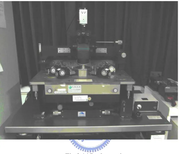
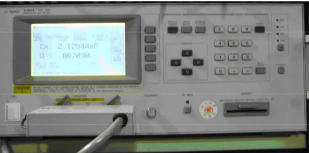
3.2 Measurement Tools
In this study, devices were put on the stage of probe station (Fig 3.14) to be measured. Capacitance-voltage(C–V) and current-voltage(I–V) characteristics were obtained using HP4284 (Fig 3.15) and HP4156 (Fig 3.16), respectively. The current – voltage characteristic measurement of thin film transistor devices was performed by HP4156 semiconductor parameter analyzer with source grounded and body floating. The thickness of dielectric is measured by Ellipometer.
3.3 Parameter Extraction
In this section, the methodology we use to extract typical parameters in TFTs such as threshold voltage, subthreshold swing, field-effect mobility µFE, and the on/off current ratio for device characteristics are briefly introduced.
3.3.1
Determination of Threshold Voltage
Threshold voltage (Vth) is an important parameter because it affect the drain current
and device drivability drastically. There are several methods to determine the threshold voltage of thin film transistors. Two of most commonly used extraction methods are the
constant drain current method and the maximum transconductance method. The constant drain current method define the voltage at a specific drain current as the threshold voltage. Typically, the threshold current is specified at (W/L) ×10nA for VDS=0.1V and (W/L) ×
100nA for VDS =5V in most papers to extract the threshold voltage of TFTs. , where W and
L are channel width and channel length, respectively. However, in this thesis we use maximum transconductance method to get our threshold voltage because it is more accurate. This techniques is the linear extrapolation method with the drain current measured as a function of gate voltage at a low drain voltage of 50~100mV to ensure operation in the linear region, and the drain current as a function of gate voltage can be reduced to
(
)
[
VDS]
th V GS V L W ox C eff DS I ⎟ − ⎠ ⎞ ⎜ ⎝ ⎛ =µ ---(Eq. 4.1)The drain current is not zero when VGS below threshold voltage and approaches zero
asymptotically. Hence the IDS versus VGS curve can be extrapolated to ID=0, and the Vth is
determined from the extrapolated intercept of gate voltage Equation (4.1) is strictly only valid for negligible series resistance. Fortunately series resistance is usually negligible at the low drain current when threshold voltage measurements are made. The IDS-VGS curve deviates
from a straight line at gate voltage below Vth due to sub-threshold current and above Vth due
to series resistance and mobility degradation effects. It is common practice to find the point of maximum slope of the IDS-VGS curve and fit a straight line to extrapolate to ID=0 by means of
finding the point of maximum of transconductance (Gm).
3.3.2
Determination of Field Effect Mobility
The field-effect mobility (µFE) is determined from the transconductance gmat low
drain voltage. Usually, the maximum value of transconductance (Gm) are used to represent the
device performance. The transfer characteristics of Poly-Silicon TFTs are similar to those of conventional MOSFETs, so that the first order of I-V relation in the bulk Si MOSFETs can be applied to Poly-Silicon TFTs. The drain current in linear region (VDS<VGS-Vth) can be
approximated as the following equation:
(
)
⎥⎦⎤ ⎢⎣ ⎡ − − ⎟ ⎠ ⎞ ⎜ ⎝ ⎛ = 2 2 1 DS V DS V th V GS V L W ox C eff DS I µ ---(Eq. 4.2)where Cox is the gate oxide capacitance per unit area, Vth is the threshold voltage, and W and L are channel width and channel length, respectively. Therefore, the transconductance is given by DS V L W ox C eff GS V DS I m g ⎟ ⎠ ⎞ ⎜ ⎝ ⎛ = ∂ ∂ = µ ---(Eq. 4.3)
Therefore, the field-effect mobility is 0 (max) → = DS V m g DS WV ox C L eff µ ---(Eq. 4.4)
3.3.3
Determination of Sub-threshold Slope
Sub-threshold slope (S.S.) is a typical parameter to describe the control ability of gate toward channel, which reflects the turn on/off speed of a device. It is defined as the amount of gate voltage required to increase/decrease drain current by one order of magnitude. The S.S. should be independent of drain voltage and gate voltage. However, in reality, the S.S. increases with drain voltage due to channel shortening effect such as charge sharing, avalanche multiplication and punchthrough effect. The sub-threshold slope is also related to gate voltage due to undesirable and inevitable factors such as the serial resistance and interface states. In this thesis, the S.S. is defined as one-third of the gate voltage required to decrease the threshold current by three orders of magnitude. The threshold current is specified to be the drain current when the gate voltage is equal to threshold voltage.
3.3.4
Determination of ON/OFF Current Ratio
On/Off current ratio is one of the most important parameters of poly-Si TFTs especially in the application of LCD because It affects the bright and dark states of TFTs screens drastically. The leakage current mechanism in poly-Si. TFTs is like that in MOSFETs.
But, in MOSFETs, the channel is composed of single crystalline Si and the leakage current is due to the tunneling of minority carrier from drain region to accumulation layer located in channel region. In poly-Si TFTs, the channel is composed of poly-Si. A large amount of trap state densities in grain structure attribute a lot of defect states in energy band gap to enhance the tunneling effect. Therefore, the leakage current is much larger in poly-Si TFTs than in MOSFETs. When the voltage drops between gate voltage and drain voltage increases, the band gap width decreases and the tunneling effect becomes much more severe. Normally we can find this effect in typical Poly-Silicon TFT’s IDS-VGS characteristics where the magnitude
of leakage current will reach a minimum and then increase as the gate voltage decreases/increases for n/p-channel TFTs. There are a lot of ways to specify the on and off-current. In this chapter, take n-channel poly-Si TFTs for examples, the on-current is defined as the drain current when gate voltage at the maximum value and drain voltage is 0.1V. The off-current is specified as the minimum current when drain voltage equals to 0.1V.
V V at Plot V I of Current Minimum V V at Plot V I of Current Maximum I I DS GS DS DS GS DS off on 1 . 0 1 . 0 = − = − = ---(Eq.4.5)
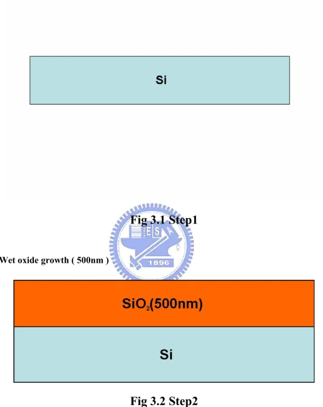
1. Silicon substrate (RCA Clean)
Fig 3.1 Step1
2. Wet oxide growth ( 500nm )
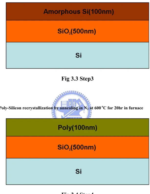
3. Amorphous Silicon deposition by LPCVD at 550 oC
Fig 3.3 Step3
4. Poly-Silicon recrystallization by annealing in N2 at 600 oC for 20hr in furnace
5. Isolation oxide deposition by PECVD ( 500nm )
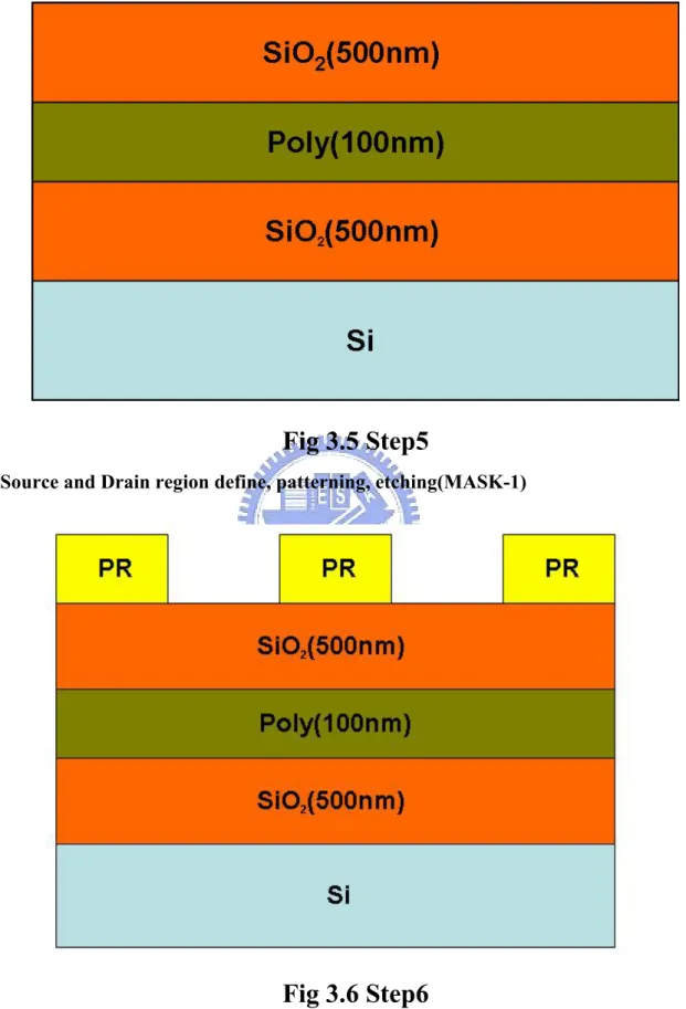
Fig 3.5 Step5
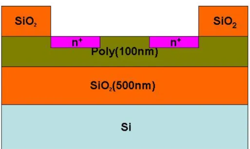
6. Source and Drain region define, patterning, etching(MASK-1)
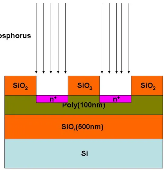
7. Source and Drain implantation with phosphorus(35kev at 5E15 cm-2)
8. Activation in N2 at 600oC for 12hr.
9. Removing Silicon oxide on gate region ( MASK-2)
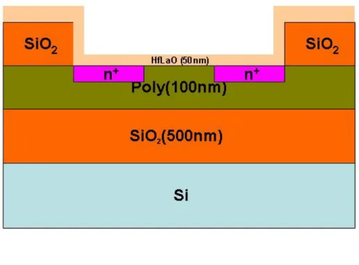
10. HfLaO deposition by PVD and 500oC PDA
Fig 3.9 Step9
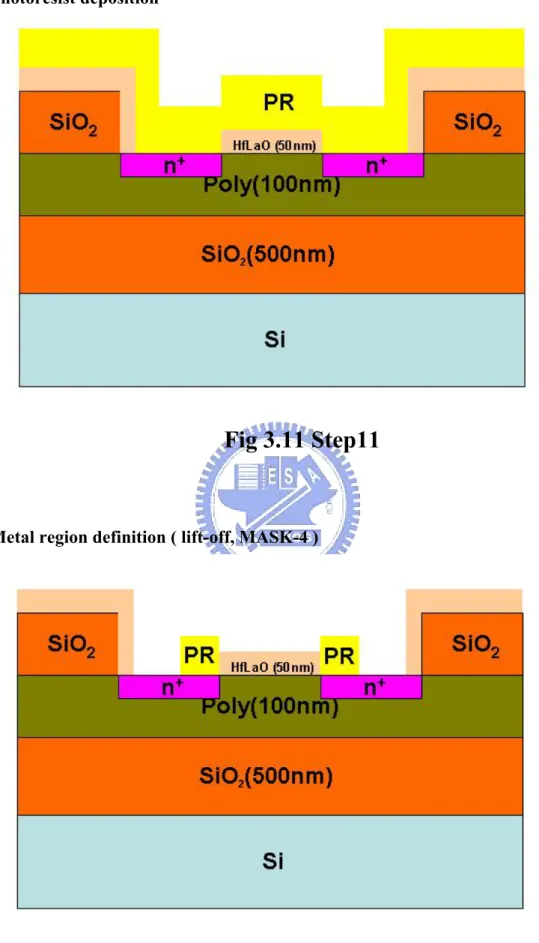
11. Contact hole, patterning, etching (MASK-3)
12. Photoresist deposition
Fig 3.11 Step11
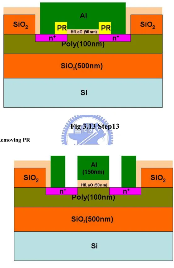
13. Metal region definition ( lift-off, MASK-4 )
14. PVD-Al deposition ( 150nm )
Fig 3.13 Step13
15. Removing PR
Chapter 4
Result & Discussion
4.1
Experimental Data Result & Discussion
The electrical characteristics of fabricated devices were measured by Agilent 4156 Precision Semiconductor Parameter Analyzer and Agilent 4284 LCR meter. The physical thickness of these high-κ films were confirm by Ellipsometer. The first three Figures (Fig 4-1 ~ Fig 4-3) show C-V characteristic of Al/HfLaO/Si capacitors with La ratio from 20% ~ 40%. From the C-V curve, we get the EOT of HfLaO is around 8.5 ~ 9.1 nm, which is the thinnest reported EOT in the application of TFTs so far. Combining the EOT with a physical thickness of 50 nm, the dielectric constant of this PVD HfLaO is about 22, which is a high value to overcome the more severe gate leakage current problem compared to MOSFETs. The normalized C-V curve of Al/HfLaO/Si capacitors different La ratio from 20% ~ 40% were shown in Fig. 4.4. It is obvious that the flatband voltage was more negative with the increase of contained La. The output characteristics (Id-Vd) of the Al/HfLaO TFTs with channel length
of 10 µm are shown from Fig. 4.5 to Fig. 4.7 . The large drive current of 800 ~ 1200 µA at 5V is attractive for high-speed display ICs. The threshold voltage of our devices were extracted using the method of tangent line on the Id-Vg curve at the point of maximum transconductance
threshold voltage were 1.13V, 1V, 0.835V which is better than the threshold voltage of the device with different dielectric materials which were reported before ( Table 4.1 ). The threshold voltage decreases because that La in the dielectric makes the more negative flatband voltage . Base on the threshold voltage equation:
(
)
fp FB ox SD TN V C Q V = ′ (max) + +2φMore negative VFB makes lower threshold voltage. And in Fig 4.11 ~ Fig 4.13, we can see
the sub-threshold slope of nearly 500 mV/decade, giving the good electron field-effect mobility of 30.79 cm2/Vs (for La/La+Hf = 40%) for all these devices. The good sub-threshold swing and mobility indicate a low interface trap density. The Ion / Ioff ratio of the Al/HfLaO
TFT is about 106, even without performing hydrogen passivation. This good performance is related to the lower threshold voltage and the high gate-capacitance of from C-V measurements, which gives a small equivalent-oxide thickness (EOT) and a high κ value , And the high drive current is higher than compared to other reported thin film transistor (Table 1). It is because the Lanthanide in the high-κ layer makes the flat band voltage very lower even using aluminum as the gate electrode which work function is 4.1eV. So the data affirm our conception. Our design also provides an alternative way to create high drive current, along with existing approaches such as excimer-laser crystallization (ELC), metal-induced lateral crystallization and electric field enhanced crystallization. It shows that good uniformity is also obtained due to the furnace crystallization, in contrast with the narrow
process window and poor uniformity in ELC TFTs. The field dependence of the gate current density is showed in Fig 4.14 ~ Fig 4.16 shows a gate dielectric breakdown electric field can up to 7 MV/cm. This is high enough to drive a liquid crystal display. This high breakdown field is comparable with or better than that for PECVD TEOS oxide. This is important for achieving good dielectric reliability. It may arise from the robust quality of HfLaO film and the plasma-free process used, which does not damage the gate dielectric. Hence integrating high-κ gate dielectrics HfLaO into TFT-NMOS should not degrade the TFT device reliability, often dominated by the grain-boundary related hot-carrier degradation. The important device parameters are summarized in Table 1. The better device performance of the Al/HfLaO TFTs that compared with other structure is due to the lower threshold voltage which results from the higher capacitance density combining with the plasma-free process.
-3.0 -2.5 -2.0 -1.5 -1.0 -0.5 0.0 0.5 1.0 0.0 0.1 0.2 0.3 0.4 0.5
La/La+Hf= 20%
C
ap
aci
ta
n
c
e
(
uF/cm
2)
Voltage (V)
Al/HfLaO/Si
-3.0 -2.5 -2.0 -1.5 -1.0 -0.5 0.0 0.5 1.0 0.0 0.1 0.2 0.3 0.4 0.5
Al/HfLaO/Si
La/La+Hf= 30%
C
ap
aci
ta
n
c
e
(
uF/cm
2)
Voltage (V)
-3.0 -2.5 -2.0 -1.5 -1.0 -0.5 0.0 0.5 1.0 0.0 0.1 0.2 0.3 0.4 0.5
Al/HfLaO/Si
La/La+Hf= 40%
C
ap
aci
ta
n
c
e
(
uF/cm
2)
Voltage (V)
-3.0 -2.5 -2.0 -1.5 -1.0 -0.5 0.0 0.5 1.0 0.0 0.2 0.4 0.6 0.8 1.0 La/La+Hf= 20% La/La+Hf= 30% La/La+Hf= 40%
Ca
pa
ci
ta
nc
e
(
uF/cm
2)
Voltage (V)
Fig 4.4 Normalized C-V of Al/HfLaO/Si capacitor with different La ratio from 20% ~ 40%
0 1 2 3 4 5 6 0.0 0.2 0.4 0.6 0.8 1.0 VG=5 V VG=3 V VG=1 V La/La+Hf= 20% W/L= 100 um/10 um Dr a in Curr ent ( m A) Drain Voltage (V)
0 1 2 3 4 5 6 0.0 0.2 0.4 0.6 0.8 1.0 1.2 VG=5 V V G=3 V VG=1 V La/La+Hf= 30% W/L= 100 um/10 um Drai n Current ( m A ) Drain Voltage (V)
0 1 2 3 4 5 6 0.0 0.2 0.4 0.6 0.8 1.0 1.2 1.4 La/La+Hf= 40% W/L= 100 um/10 um D rai n Cur rent ( m A ) Drain Voltage (V) V G=5 V V G=3 V V G=1 V Fig 4.7 Id-Vd characterisitic of Al/HfLaO/Si TFT with La ratio of 40%
0 1 2 3 4 5 0 10 20 La/La+Hf= 20% W/L= 100 um/10 um Vd = 0.1 V Vt ~ 1.13 V Voltage (V) Drai n Cu rrent ( u A) 0 1 2 3 4 5 Gm ( u A/ V)
Fig 4.8 Id-Vd and transconductacne characterisitic of Al/HfLaO/Si TFT with La ratio of 20%
0 1 2 3 4 5 0 10 20 30 40 Voltage (V) D rai n Cu rr ent ( u A ) La/La+Hf= 30% W/L= 100 um/10 um Vd = 0.1 V Vt ~ 1.0 V 0 2 4 6 8 10 Gm ( u A /V)
Fig 4.9 Id-Vd and transconductacne characterisitic of Al/HfLaO/Si TFT with La ratio of 30%
0 1 2 3 4 5 0 8 16 24 32 40 La/La+Hf= 40% W/L= 100 um/10 um Vd = 0.1 V Vt ~ 0.835 V Voltage (V) Drai n Cu rrent ( u A) 0 2 4 6 8 10 12 14 Gm ( u A/ V)
Fig 4.10 Id-Vd and transconductacne characterisitic of Al/HfLaO/Si TFT with La ratio of 40%
-2 -1 0 1 2 3 4 5 10-11 10-10 10-9 10-8 10-7 10-6 10-5 10-4 La/La+Hf= 20% W/L= 100 um/10 um Vd = 0.1 V D rai n Curre nt (A) Gate Voltage (V)
Subthreshold Swing ~ 530 mV/dec On/Off ratio ~ 1.2 x 10⁶
-2 -1 0 1 2 3 4 5 10-11 10-10 10-9 10-8 10-7 10-6 10-5 10-4 La/La+Hf= 30% W/L= 100 um/10 um Vd = 0.1 V Drain Cu rren t (A) Gate Voltage (V)
Subthreshold Swing ~ 518 mV/dec On/Off ratio ~ 1.01 x 10⁶
-2 -1 0 1 2 3 4 5 10-11 10-10 10-9 10-8 10-7 10-6 10-5 10-4 La/La+Hf= 40% W/L= 100 um/10 um Vd = 0.1 V D ra in C urrent ( A ) Gate Voltage (V)
Subthreshold Swing = 508 mV/dec On/Off ratio = 1.3 x 10⁶
0 1 2 3 4 5 6 7 8 10-7 10-6 10-5 10-4 10-3 10-2 10-1 100 101 Al/HfLaO/Si La/La+Hf= 20% Cur re n t Den s ity ( A/c m 2 ) Electrical Field (MV/cm) Breakdown Field ~ 7 MV/cm
0 1 2 3 4 5 6 7 8 10-7 10-6 10-5 10-4 10-3 10-2 10-1 100 101 Al/HfLaO/Si La/La+Hf= 30% Breakdown Field ~ 6.8 MV/cm Cur rent D e nsit y
(
A/cm 2)
Electrical Field (MV/cm)0 1 2 3 4 5 6 7 8 10-7 10-6 10-5 10-4 10-3 10-2 10-1 100 101 Al/HfLaO/Si La/La+Hf= 40% Breakdown Field ~ 6.6 MV/cm Cur rent D e nsit y
(
A/cm 2)
Electrical Field (MV/cm)Gate dielectric This work HfLaO (La 40%) LPCVD SiO2 80nm [28] PECVD TEOS Oxide 60nm [29] PECVD TEOS Oxide 40nm [30] Al2O3 50nm [30] Gate
electrode Aluminum Poly-Si Poly-Si Poly-Si Poly-SiGe
Vth(V) 0.835 5.6 8.14 Not extracted 3 µFE (cm2/V s) 30.79 20 12.44 3 47 Sub-threshold Slope (V/decade) 0.508 1.4 1.97 2.67 0.44 Ion/Ioff 1.3×10⁶ 3.5×10⁵ 2.97×10⁵ Not extracted 3×10 5 Breakdown Field (MV/cm) 6.6 Not extracted Not extracted 5.4 Not extracted Table 1
Chapter 5
Conclusion
A new high-κ dielectric TFT with HfLaO as the gate insulator structure has been proposed and successfully fabricated. The process is simple and compatible to conventional LTPS process. Our experimental data show that the new new high-κ dielectric TFT has higher turn-on current, on/off current ratio and excellent current saturation characteristics at high bias, compared to the conventional TFT. That is due to the high-κ value and robust quality of HfLaO film itself and the plasma-free process used, which does not damage the gate dielectric. The new structure is therefore ideally suitable for implementing high-density and high-performance driver circuits on the glass panel for AM-LCD applications. This is because that our TFT device has lower threshold voltage, low subthreshlod slope, high field effect mobility lower leakage current, good breakdown voltage, higher turn-on current and on/off current ratio.
Chapter 6
Reference
[1] M. Koyama, K. Suguro, M. Yoshiki, Y. Kamimuta, M. Koike, M. Ohse, C. Hongo
and A. Nishiyama, “Thermally stable ultra-thin nitrogen incorporated ZrO2 gate
dielectric prepared by low temperature oxidation of ZrN” in IEDM Tech. Dig.,2001, pp. 20.3.1-20.3.4.
[2] E. P. Gusev, D. A. Buchanan, E. Cartier, A. Kumar, D. DiMaria, S. Guha, A. Callegari, S. Zafar, P. C. Jamison, D. A. Neumayer, M. Copel, M.A. Gribelyuk, H. Okorn-Schmidt, C. D Emic, P. Kozlowski, K. Chan, N. Bojarczuk, L.-A.
Ragnarsson and Rons, “Ultrathin high-κ gate stacks for advanced CMOS
devices” in IEDM Tech. Dig., 2001, pp. 20.1.1-20.1.4.
[3] W.Zhu, T. P. Ma, T. Tamagawa, Y. Di, J. Kim, R. Carruthers, M. Gibson and T.
Furukawa, “HfO2 and HfAlO for CMOS: thermal stability and current
transport” in IEDM Tech. Dig., 2001, pp. 20.4.1-20.4.4.
[4] L. Kang, K. Onishi, ?Y. Jeon, Byoung Hun Lee, C. Kang, Wen-Jie Qi, R. Nieh, S. Gopalan, R Choi and J. C. Lee, “MOSFET devices with polysilicon on single-layer HfO2 high-κ dielectrics” in IEDM Tech. Dig., 2000, pp.35-38
[5] Rino Choi, Chang Seok Kang, Byoung Hun Lee, K. Onishi, R. Hieh, S. Gopalan,
MOSFETs with TaN electrode and nitridation surface preparation” in IEDM Tech. Dig., 2001, pp. 15-16.
[6] Z. J. Luo, T. P. Ma, E. Cartier, M. Copel, T. Tamagawa and B. Halpern,
“Ultra-thin ZrO2 (or silicate) with high thermal stability for CMOS gate
applications” in Symp on VLSI Technology, 2001, pp. 135-136. [7] International Technology Roadmap for Semiconductor, 2006.
[8] J. K. Schaeffer, C. Capasso, L. R. C. Fonseca, S. Samavedam, D. C. Gilmer, Y. Liang, S. Kalpat, B. Adetutu, H.-H. Tseng, Y. Shiho, A. Demkov, R. Hegde, W. J. Taylor, R. Gregory, J. Jiang, E. Luckowski, M. V. Raymond, K. Moore, D. Triyoso, D. Roan, B. E. White Jr, and P. J. Tobin, “Challenges for the integration of metal gate electrodes,” in IEDM Tech. Dig., 2004, pp. 287-290
[9] W. P. Maszara, Z. Krivokapic, P. King, J. S. Goollgweon, and M. R. Lin, “Transistors with dual work function metal gate by single full silicidation (FUSI) of polysilicon gates,” in IEDM Tech. Dig, 2002, pp.367-370.
[10] H.-H. Tseng, C. C. Capasso, J. K. Schaeffer, E. A. Hebert, P. J. Tobin, D. C. Gilmer, D. Triyoso, M. E. Ramón, S. Kalpat, E. Luckowski, W. J. Taylor, Y. Jeon, O. Adetutu, R. I. Hegde, R. Noble, M. Jahanbani, C. El Chemali, and B. E. White, “Improved short channel device characteristics with stress relieved pre-oxide (SRPO) and a novel tantalum carbon alloy metal gate/HfO2 stack,” in
IEDM Tech. Dig., pp. 821-824, 2004.
[11] H. -J. Cho, C. S. Kang, K. Onishi, S. Gopalan, R. Nieh, R. Choi, E. Dharmarajan and J.C. Lee, “ Novel nitrogen profile engineering for improved TaN/HfO2 Si MOSFET performance,” in IEDM Tech. Dig., pp. 30.2.1-30.2.4, 2001.
[12] Y. T. Hou, M. F. Li, T. Low, and D. L. Kwong, “ Impact of metal gate work function on gate leakage of MOSFETs,” in DRC Symp., pp. 154-155, 2003.
[13] Dae-Gyu Park, Kwan-Yong Lim, Heung-Jae Cho, Tae-Ho Cha, Joong-Jung Kim, Jung-Kyu Ko, Ins-Seok Yeo and Jin Won Park, “ Novel damage-free direct metal gate process using atomic layer deposition,” in Symp. on VLSI Technology, pp. 65-66, 2001.
[14] C. Cabral Jr. , J. Kedzierski, B. Linder, S. Zafar, V. Narayanan, S. Fang, A. Steegen, P. Kozlowski, R. Carruthers, and R. Jammy,” Dual workfunction fully silicided metal gates,” in Symp. on VLSI Technology, pp. 184-185, 2004.
[15] S. B. Samavedam, L. B. La, J. Smith, S. Dakshina-Murthy, E. Luckowski, J. Schaeffer, M. Zavala, R. Martin, V. Dhandapani, D. Triyoso, H. H. Tseng, P. J. Tobin, D. C. Gilmer, C. Hobbs, W. J. Taylor, J. M. Grant, R. I. Hegde, J. Mogab, C. Thomas, P. Abramowitz, M. Moosa, J. Conner, J. Jiang, V. Arunachalarn, M. Sadd, B.-Y. Nguyen, and B. White,” Dual-metal gate CMOS with HfO2 gate dielectric,” in IEDM Tech. Dig., pp. 433-436, 2002.
[16] D. S. Yu, A. Chin, C. C. Laio, C. F. Lee, C. F. Cheng, W. J. Chen, C. Zhu, M.-F. Li, S. P. McAlister, and D. L. Kwong, “3D GOI CMOSFETs with novel IrO2 (Hf)
Dig., pp. 181-184, 2004.
[17] D. S. Yu , A. Chin, C. C. Liao, C. F. Lee, C. F. Cheng, M. F. Li, Won Jong Yoo,
and S. P. McAlister, “3D Metal-Gate/High- /GOI C MOSFETs on
1-Poly-6-Metal 0.18-um Si Devices,” IEEE Electron Device Lett. 26, pp. 118-120, Feb. 2005.
[18] X. P. Wang, C. Shen, Ming-Fu Li, H.Y. Yu, Yiyang Sun, Y. P. Feng, Andy Lim, Hwang Wan Sik, Albert Chin, Y. C. Yeo, Patrick Lo, and D.L. Kwong,” Dual
Metal Gates with Band-Edge Work Functions on Novel HfLaO High- Gate
Dielectric,” in Symp. on VLSI Technology, pp. 12-13, 2006.
[19] J. H. Lee, H. Zhong, Y.-S. Suh, G. Heuss, J. Gurganus, B. Chen, and V. Misra,” Tunable work function dual metal gate technology for bulk and nonbulk CMOS,” in IEDM Tech. Dig., pp. 359-362, 2002.
[20] H. Y. Yu, M. F. Li, and D.L. Kwong,” Thermally Robust HfN Metal as a Promising Gate Electrode for Advanced MOS Device Application,” IEEE Transactions on Electron Devices, vol. 51, Apr., 2004.
[21] A. Veloso, K. G. Anil, L. Witters, S. Brus, S. Kubicek, J.-F. de Marneffe,
B. Sijmus, K. Devriendt, A. Lauwers, T. Kauerauf, M. Jurczak, and
S. Biesemans, “Work function engineering by FUSI and its impact on the performance and reliability of oxynitride and Hf-silicate based MOSFETs,” in IEDM Tech. Dig., pp. 855-858, 2004.
[22] S. J. Rhee, C. S. Kang, C. H. Choi, C. Y. Kang, S. Krishnan, M. Zhang, M. S. Akbar, and J. C. Lee, “Improved electrical and material characteristics of hafnium titanate multi-metal oxide n-MOSFETs with ultra-thin EOT (~8Å) gate dielectric application,” in IEDM Tech. Dig., pp.837-840, 2004.
Liao, “Very high _ and high density TiTaO MIMcapacitorsfor analog and RF applications,” in Symp. VLSI Tech. Dig., 2005, pp.62–63.
[24] D. S. Yu, A. Chin, C. H. Wu, M.-F. Li, C. Zhu, S. J. Wang, W. J. Yoo, B. F. Hung, and S. P. McAlister, “Lanthanide and Ir-based dual metalgate/ HfAlON CMOS with large work-function difference,” in IEDM Tech. Dig., 2005, pp. 649–652. [25] C. H. Huang, D. S. Yu, A. Chin, W. J. Chen, C. X. Zhu, M.-F. Li, B. J. Cho, and
D. L. Kwong, “Fully silicided NiSi and germanided NiGe dual gates on SiO2/Si and Al2O3/Ge-on-insulator MOSFETs,” in IEDM Tech. Dig., 2003, pp. 319–322. [26] B. Tavel, T. Skotnicki, G. Pares, N. Carrière, M. Rivoire, F. Leverd, C. Julien, J.
Torres, and R. Pantel, “Totally silicided (CoSi2) polysilicon: A novel approach to very low-resistive gate (∼2Ω/_) without metal CMP nor etching,” in IEDM Tech. Dig., 2001, pp. 815–828.
[27] T. Nabatame, M. Kadoshima, K. Iwamoto, N. Mise, S. Migita, M. Ohno, H. Ota, N. Yasuda, A. Ogawa, K. Tominaga, H. Satake, and A. Toriumi, “Partial silicides technology for tunable work function electrodes on high-κ gate dielectrics- fermi level pinning controlled PtSix for HfOx(N) pMOSFET,” in IEDM Tech. Dig., 2004, pp. 83–86.
[28] Y. W. Choi, J. N. Lee, T. W. Jang, and B. T. Ahn, “Thin-film transistors fabricated with poly-Si films crystallized at low temperature by microwave