國
立
交
通
大
學
電 機 與 控 制 工 程 學 系
博 士 論 文
高輕載轉換效率及最小互穩壓特性之
單電感多輸出直流-直流轉換器
Single-Inductor Multi-Output (SIMO) DC-DC Converters
with High Light-Load Efficiency and Minimized Cross-Regulation
研 究 生:黃銘信
指導教授:陳科宏 副教授
高輕載轉換效率及最小互穩壓特性之
單電感多輸出直流-直流轉換器
Single-Inductor Multi-Output (SIMO) DC-DC Converters
with High Light-Load Efficiency and Minimized Cross-Regulation
研 究 生:黃銘信 Student:Ming-Hsin Huang
指導教授:陳科宏 Advisor:Dr. Ke-Horng Chen
國 立 交 通 大 學
電 機 與 控 制 工 程 學 系
博 士 論 文
A Thesis
Submitted to Department of Electrical and Control Engineering
College of Electrical Engineering National Chiao Tung University
in partial Fulfillment of the Requirements
for the Degree of Doctor
in
Electrical and Control Engineering
March 2009
Hsinchu, Taiwan, Republic of China
高 輕 載 轉 換 效 率 及 最 小 互 穩 壓 特 性 之
單 電 感 多 輸 出 直 流 -直 流 轉 換 器
研究生:黃銘信
指導教授 陳科宏 副教授
國立交通大學電機與控制工程學系 (研究所) 博士班
摘 要
本 論 文 提 出 可 同 時 提 供 降 壓 (buck) 及 升 壓 (boost) 輸 出 電 源 準 位 並 具 磁 滯 模 式(hysteresis mode)與負載電流相依式峰值電流控制(load-dependant peak-current control,
LDPCC)機制之單電感多輸出直流-直流電源轉換器(single-inductor multi-output converter,
SIMO converter)。在 LDPCC 機制及磁滯(hysteresis)模式的自動調節功能控制之下,各個 輸出端的互穩壓(cross regulation)效應可被有效的降低。此外,新發表的壓差產生電路
(delta-voltage generator)與功率比較器(power comparator)的控制下,SIMO 電源轉換器能 平順地在脈寬調變(pulse width modulation, PWM)操作模式與磁滯模式之間切換,故能有
效消除當降壓端的輸出功率大於升壓端的輸出功率情形下所產生的電感電流累積效
應。本論文所發表的 SIMO 直流電源轉換器使用了 TSMC 0.25μm 2P5M 製程來實現驗証
晶片的設計。驗証晶片的實驗結果呈現出在磁滯模式下有 80%的輕載轉換效率及脈寬調
變模式下 93%的重載轉換效率,並可得到最小互穩壓效應可減少至 0.35%的輸出電壓準
位之內。
關鍵字:單電感多輸出直流電源轉換器(SIMO converter),互穩壓效應(cross regulation),
Single-Inductor Multi-Output (SIMO) DC-DC Converters
with High Light-Load Efficiency and Minimized Cross-Regulation
Student: Ming-Hsin Huang
Advisor: Dr. Ke-Horng Chen
Department of Electrical and Control Engineering
National Chiao-Tung University
Abstract
A load-dependant peak-current control single-inductor multiple-output (SIMO) converter
with hysteresis mode is proposed. It includes multiple buck and boost output voltages. Owing
to the adaptive adjustment of the load-dependant peak-current control technique and the
hysteresis mode, the cross-regulation can be minimized. Furthermore, a new delta-voltage
generator can automatically switch the operating mode from pulse width modulation (PWM)
mode to hysteresis mode, thereby avoiding inductor current accumulation when the total
power of the buck output terminals is larger than that of the boost output terminals. The
proposed SIMO converter was fabricated by TSMC 0.25μm 2P5M technology. The
experimental results show high conversion efficiency at light loads and small cross-regulation
within 0.35%. The power conversion efficiency varies from 80% at light loads to 93% at
heavy loads.
Keywords—Single-inductor multi-output (SIMO) converter, cross-regulation, and hysteresis
誌 謝
行文至此,意味著博士生涯的落幕。在這漫長的博班研讀期間,在校的課程學習、 產學合作的研究經歷以及在業界的工作經驗,讓我切切實實地成長為一名獨立自主的研 究人員。終於,今年的鳳凰花開對我有著不同意義,不再是督促自我的警剔,而是滿載 著離別的愁緒與燦紅的祝福。 如今能順利取得博士學位,感謝 陳科宏教授。那年,在我為研究方向困頓不已之 時修了您的課,成了我博士生涯的轉捩點。您那股對實務研究的堅持與熱情一直是我感 佩與企求的境地,您總是能在談笑間開拓我的思維,給予我在研究上最大的包容與信 賴,引領我前往更寬闊精深的研究領域。每次與您的對話所得的不僅是學術上的洗禮, 更是實務技術上的沈積。論文及 PAPER 的產出過程,有您一路指引,感激難以言表。 感謝口試委員 郭斯彥教授、 潘晴財教授、 王清松教授、 黃立仁副總、 鄒應嶼 教授及 陳福川教授在口試期間對論文的指導與斧正,使得論文能更瑧完善,讓我在幾 度峰迴路轉後又見曙光,有了您們寶貴的意見,自己才能對整份研究有了更深切的感知。 感謝與我共事研究、為我擔待的實驗室伙伴們:裕農、 小柯、 國林、 逢哥、 漢 翔、 均元、 福龍、 東樺、 君晏,這幾年你們的下線時程總是因我的研究變得不盡合 理,謝謝你們毫無怨言、全心全力的配合。還有 謝小乖、 昱輝,謝謝你們願意與我相 互分享、討論研究的想法,減少探索研究議題的時間。感謝 小契,每每與我在實驗室 挑燈到午夜。 感謝一路相守的 彥君,有妳的耳提面命,我才能不忘作為一個學生的本分,不致 迷失在茫茫的學海之中,有妳的支持鼓勵,我才能筆直向前,努力不懈,相信這一切的 過程值得我們一輩子咀嚼回味。感謝 爸媽、 岳父母以及我的家人,是你們默默的支持 及守護,讓我可以毫無迭躂地走完博士研究的道路。感謝伴隨在我週遭的朋友,你們的 鼓勵與陪伴,給了我不少的動力。 誠如 陳之藩先生於謝天一文所述的:「真正做了一些小貢獻以後,才有了一種新 的覺悟:即無論什麼事,得之於人者太多,出之於己者太少。因為需要感謝的人太多了,就感謝天罷。無論什麼事,不是需要先人的遺愛與遺產,即是需要眾人的支持與合作, 還要等候機會的到來。越是真正做過一點事,越是感覺自己的貢獻之渺小。」 感謝天,讓我立足於此,佔有一席,沒有因為挫折壓力而放棄求學的道路。感謝天, 付予我堅強的勇氣和毅力,讓我能在研究學習的長河中喘息。最後,感謝這一直伴隨我 的校園長廊,一如往昔地聆聽著我低聲的獨語。 黃銘信 謹誌 國立交通大學 電機與控制學系 二○○九 初春
Contents
Chinese Abstract ... i
Abstract ... ii
Acknowledgement ... iii
Contents ... v
Figure Captions ... vii
Table Captions... xiii
Chapter 1 Introduction... 1
1.1 Background ... 1
1.2 Prior Arts ... 3
1.3 Motivation ... 21
1.4 Thesis Organization ... 21
Chapter 2 Minimum Switch Number Structure with the Load-Dependant Peak-Current Control Technique ... 22
2.1 Controlling Sequence Used to Minimize the Number of Switches... 22
2.2 LDPCC Method for Improving Light-Load Efficiency, Stability, and Cross-Regulation ... 30
2.3 System Architecture of SIMO DC-DC Converter ... 35
Chapter 3 Design and Analysis of Proposed SIMO DC-DC Converter ... 38
3.1 LDPCC Decision Circuit... 38
3.2 Current Sensor and Charge Reservation Circuits ... 41
3.3 Logic Control Circuit with Automatic Mode Switch for Avoiding Instability Problem ... 47
3.4 Clock Generator with Power-On Reset Mechanism and Startup Circuit... 53
3.5 Dead-time Controller and Driver... 57
3.6 Maximum Voltage Selector Circuit and Adaptive Body Switch (ABS) Circuit ... 60
3.7 Reference Voltage and Power-On Reset Circuit... 67
Chapter 4 Power Comparator and Delta-Voltage Generator... 70
4.2 Delta-Voltage Generator... 74
Chapter 5 Measurement Results ... 78
Chapter 6 Conclusions and Future Works... 88
6.1 Conclusions ... 88
6.2 Future Works ... 90
References... 91
Published Paper ... 98
Figure Captions
Fig. 1. The power management designs which uses LDO array. ... 2
Fig. 2. The power management designs which combines with different inductive switching converters... 2
Fig. 3. The conceptual SIMO converter uses only one external inductor component to generate multiple voltage levels... 3
Fig. 4. The physical behavior of single-inductor multiple positive/negative output dual-loop DC-DC converter. ... 5
Fig. 5. The implementation of output power stage. ... 5
Fig. 6. The state machine determines the operating pattern of output power stage... 6
Fig. 7. The adaptive peak current control is applied to directly couple to output loads and adjust accordingly to state machine... 6
Fig. 8. The QC method which works in PCCM to regulate one buck and one boost output. ... 9
Fig. 9. The corresponding timing diagram of QC method. ... 9
Fig. 10. The inductor current waveform of QC control method... 10
Fig. 11. The architecture of dual output DCM converter with TM control method [3]... 12
Fig. 12. The timing diagram of TM control method [10]... 13
Fig. 13. The architecture of PCCM control mode for SIDO converter which [10]... 13
Fig. 14. The synchronous boost converter with freewheeling current feedback [24]... 16
Fig. 16. The five-output SIMO converter with OPDC in [13]. ... 19
Fig. 17. The timing diagram of OPDC operation. ... 20
Fig. 18. The inductor current of different load conditions. ... 20
Fig. 19. An example of the load condition changes in Vo3. ... 20
Fig. 20. The behavior of conventional SIDO converter with one buck and one boost output in [2, and 12]. ... 23
Fig. 21. The inductor current waveform of conventional control sequence [3 and 10]... 24
Fig. 22. The topology of minimum number of switches in [2] with one buck and one boost output voltage... 25
Fig. 23. The previous proposed controlling sequence-I in [2]... 25
Fig. 24. The cross-regulation and inductor current waveform of SIDO converter when the load changes from light to heavy at output terminal VOA in [2]. ... 26
Fig. 25. The proposed sequence-II with LDPCC technique which eliminates the undesired value of inductor current level. ... 28
Fig. 26. The proposed controlling sequence and path 0 of the hysteresis mode control. ... 29
Fig. 27. The inductor current waveform in DCM operation when the load current changes from light to heavy load conduction. ... 31
Fig. 28. The inductor current waveform in CCM operation when the load current changes from light to heavy load conduction. ... 31
Fig. 29. The inductor current waveform in PCCM operation of work [2] when the load current changes from light to heavy load conduction. ... 33
Fig. 30. The inductor current waveform in proposed LDPCC technique operation when the
load current changes from light to heavy load conduction... 33
Fig. 31. The inductor current variation when the load condition changes from light to heavy in
output terminal VOA. ... 34
Fig. 32. The inductor current variation when the load condition changes from light to heavy in
output terminal VOB. ... 34
Fig. 33. The proposed load-dependent peak current control SIMO DC-DC converter with
hysteresis mode for high power conversion efficiency and minimum cross regulation.
... 36
Fig. 34. The implementation of the proposed LDPCC circuit which dynamically adjusts the
peak current level according to the value of load current... 38
Fig. 35. The transient simulation result of proposed LDPCC circuit which uses dual-error
output signals as an example... 40
Fig. 36. The current sensor of [2 and 3] is composed by a fully symmetrical matching structure.
... 41
Fig. 37. The simulation result of current sensor. ... 42
Fig. 38. The proposed charge reservation circuits and charge monitor circuit for reducing
output ripple. ... 43
Fig. 39. The simulation result of the proposed charge reservation circuit. ... 47
Fig. 40. The control logic generator with the mode switch controller. ... 48
Fig. 42. The simulated waveforms of control logic circuit in PWM mode operation. ... 52
Fig. 43. The simulated waveforms of control logic circuit in hysteresis mode operation. ... 52
Fig. 44. The clock generator with power-on reset control machine. ... 54
Fig. 45. The simulated waveforms of sawtooth and clock signals. ... 54
Fig. 46. The startup circuit for SIMO converter. ... 56
Fig. 47. The simulation result of startup circuit for SIMO converter. ... 56
Fig. 48. The dead-time control sequence of SIMO converter. ... 58
Fig. 49. The dead-time control circuit of SIMO converter... 59
Fig. 50. The simulation result of dead-time controller... 59
Fig. 51. The proposed maximum voltage selector circuit for dead-time and driver circuit.... 61
Fig. 52.The non-overlapping power switches. ... 61
Fig. 53. The simulation result of maximum voltage selector circuit. ... 63
Fig. 54. The cross section of n-well CMOS process... 64
Fig. 55. The latch-up and equivalent latch-up circuit in n-well CMOS process. ... 64
Fig. 56. The proposed ABS circuit for p-MOSFET’ body bias. ... 65
Fig. 57. The simulation result of proposed ABS circuit... 66
Fig. 58. The schematic of bandgap reference circuit. ... 68
Fig. 59. The simulation result of bandgap reference circuit at five model corners. ... 68
Fig. 60. the boundary condition between the PWM and hysteresis modes... 71
Fig. 61. The schematic of proposed power comparator circuit ... 72
Fig. 63. The proposed novel delta-voltage generator is used to generate the intermediate value
according to the multiple buck output load conditions. ... 75
Fig. 64. The proposed novel delta-voltage generator is used to generate the intermediate value
according to the multiple boost output load conditions... 75
Fig. 65. The differential transconductance amplifier for the generation of the inductor current
slope... 76
Fig. 66. Micrograph of the proposed SIMO converter and the chip size is 1800*2100μm2... 78
Fig. 67. The inductor current controlling sequence measured waveform with heavy loads... 79
Fig. 68. The measurement of load regulation and cross-regulation when a stepping load (10mA
to 100mA) at the buck output terminal VOK1. ... 79
Fig. 69. The measurement of load regulation and cross-regulation when a stepping load (10mA
to 100mA) at the buck output terminal VOK2. ... 79
Fig. 70. The measurement of load regulation and cross-regulation when a stepping load (10mA
to 100mA) at the boost output terminal VOT1. ... 80
Fig. 71. The measurement of load regulation and cross-regulation when a stepping load (10mA
to 100mA) at the boost output terminal VOT2. ... 80
Fig. 72. The cross-regulation at the buck output VOK2 in the PWM and hysteresis modes... 82
Fig. 73. The cross-regulation at the boost output VOT1 in the PWM and hysteresis modes. ... 83
Fig. 74. The buck outputs operate in the PWM mode when boost outputs operate at heavy loads.
... 83
light loads... 84
Fig. 76. The boost outputs in the PWM mode when the buck outputs operate at light loads. 84
Fig. 77. The boost outputs in the hysteresis mode when the buck outputs operate at heavy loads.
... 85
Fig. 78. The output ripples estimation of buck output in the SIMO converter... 85
Fig. 79. The output ripples estimation of boost output in the SIMO converter... 86
Fig. 80. The power conversion efficiency of the SIMO DC-DC converter with the LDPCC
Table Captions
Table. I. The specific of inductor current path in conventional SIDO converter... 24
Chapter 1
Introduction
1.1 Background
Today’s field of power management requires high power conversion efficiency, fast
line/load transient response, and small volume of the power module. In particular, cell phones,
digital cameras, MP3 players, PDAs and portable products require varied voltage levels of
power supplies for delivery to different sub-modules in portable products. Thus, there are
different designs that provide different voltage levels as shown in Fig. 1~3. Low dropout
(LDO) regulator arrays are one of the designs for different voltage levels as depicted in Fig. 1,
where the index i is from 1 to n which is used to index the nth output. However, LDO
regulator arrays sacrifice power conversion efficiency and greatly reduce battery life. The
other solution is illustrated in Fig. 2, which combines with different inductive switching
converters. The high power conversion efficiency is ensured by the inductive switching
converter. However, the large number of inductors occupies the large footprint area and
increase fabrication cost.
The single inductor multiple output (SIMO) converter has been developed as a suitable
solution to achieve microminiaturization and high power conversion efficiency for a power
management unit. The conceptual SIMO converter shown in Fig. 3 uses only one external
inductor component to generate multiple voltage levels for different sub-modules in the
portable products. The SIMO converter not only reduces the footprint area and fabrication
conditions of the multiple output terminals arise in the current level of the inductor. When the
load current condition of each output accumulates in the same inductor, the design challenges
of the SIMO converter such as cross-regulation, power conversion efficiency, system stability,
and lack of flexibility of both the buck and boost must be seriously addressed.
Fig. 1. The power management designs which uses LDO array.
Fig. 2. The power management designs which combines with different inductive switching
Fig. 3. The conceptual SIMO converter uses only one external inductor component to
generate multiple voltage levels.
1.2 Prior Arts
Several topologies and control techniques have been proposed to implement SIMO
converters [2]-[13]. The SIMO converter in [1] uses the hysteretic continuous current mode
(CCM) control method and state machine to regulate output voltage. The proposed
single-inductor multiple positive/negative output dual-loop DC-DC converter illustrated in
Fig. 4 can deliver all positive and negative output voltage levels independently cycle by cycle.
The output power stage of SIMO converter depicted in Fig. 4 takes physical behavior of an
inductor which is loaded with a certain current (IPEAK) when switches A and B closed. Since
the current in the inductor is continuous, the inductor always generates a voltage with reverse
polarity across its two terminals when disconnected from the supply. For the positive inductor
node X getting open, when switch A opened and switch B closed, node X goes negative
(below ground), since the inductor tries to keep current running the same direction and
magnitude than before. Oppositely, a positive voltage (above VIN) is generated on negative
switches MN1~MNk and MP1~MPk determine which outputs VN(1)~VN(k) and VP(1)~VP(k)
can get energy stored in the inductor. When inductor is periodically loaded with current (IPEAK)
when switches A and B closed, each output VN and VP can be supported with energy cycle by
cycle. The implementation of output power stage as shown in Fig. 5 generates two positive
voltages (VGH and VBOOT) and one negative voltage (VGL). A synchronous rectifier P2 runs in
parallel to the Schottky diode D1 to enhance efficiency. A back-to-back isolated rectifiers
( N 2 D1//P2 and N 3 D2) in output multiplexers are required; otherwise to lower
positive output voltage would always clamp the higher one. An off-chip Schottky Diode D3 is
used for negative rectification. Transistors N1 and P1 connect inductor L to supply terminals.
The state machine as shown in Fig. 6 determines the operating pattern of output power
stage. Comparators Vgl, Vgh, and Vbt of each channel detect output voltage level to regulate
output voltages. Logic part of state machine takes previous states and calculates next state of
output power stage. A hysteretic control scheme which simply runs with a fixed off-time and
adaptive peak current control is applied. Since inductor always is loaded with an independent
peak current level at the beginning of off-state, output cross-regulation is negligible in
adaptive peak current control shown in Fig. 7. The frequency of adaptive peak current control
is directly coupled to output loads and adjusted accordingly to state machine. Therefore, there
are two different types of regulation loops running in the converter. A hysteretic loop is
utilized to take care of the output voltages. Hence, the control of individual channel is
managed by a state-machine controlling loop which allows hysteretic converter to run in a
pseudo-continuous current mode (PCCM) to guarantee a high power capability. The second
loop works as adaptive peak current control to minimize inductor current. It yields a small
output voltage ripple and minimized cross-regulation. Since the work proposed the
back-to-back rectifier and state-machine controller, the power dissipation and the size of
Fig. 4. The physical behavior of single-inductor multiple positive/negative output dual-loop
DC-DC converter.
IN P U T R E G IS T E R L O G IC S T A T E “ R U L E S ” O U T P U T R E G IS T E R
Fig. 6. The state machine determines the operating pattern of output power stage.
Fig. 7. The adaptive peak current control is applied to directly couple to output loads and
The work in Fig. 8 proposed a charge-control (QC) method that works in PCCM to
regulate output voltage (Voa) is lower than source voltage (Vg) and output voltage (Vob) is
higher than source voltage (Vg) [2]. Fig. 9 shows the corresponding timing diagram of QC
method. A minimum number of switches are used for the single-inductor dual-output (SIDO)
converter with QC method. At the instant of clock (φ1), switch S2 is closed and inductor
current ramps up from a freewheeling level (I1) with slope (Vg/L) until it reaches the
predefined level (IDC). Inductor is then connected to output Voa after closing switch S3a and
then clock (φa) is set to high. The inductor current (IL) continues to ramp up with a positive
slope ((Vg–Voa)/L) and is integrated by capacitor Cia of current sensor which is shown in Fig. 8.
As a result, the charge (Qoa) on capacitor Cia can be used to decide duty cycle of output Voa.
Switch S3a is opened and switch S3b is closed, the inductor is connected to output Vob and
clock (φb) is set to high. The inductor current (IL) ramps down with a negative slope
((Vob–Vg)/L) and is integrated on the capacitor Cib of current sensor which is shown in Fig. 8.
The charge (Qob) on the capacitor Cib decides the duty cycle of output Vob. Switch S3b is then
opened and switch S1 is closed, shorting out the inductor to allow freewheeling current (I1).
The inductor current waveform of QC method is shown in Fig. 10. The characteristic of
inductor current can be expressed as follows. Let the slopes (m1, m2 and m3) of inductor
current in the time intervals (t1, t2 and t3) be:
L V V m L V V m L V m1 g ; 2 g oa; 3 ob g (1) 1 1 1 m I I t DC (2)
The charge (Qoa) under time interval (t2) which depends on the load current (Ioa) of output Voa
is the charge delivered to output Voa:
I I m t
t I T Qoa DC DC 2 2 2 oa2 1
IDC m Ioa IDC
m t 2 2 2 2 1 (4)Similarly, the charge (Qob) under the time interval (t3) which depends on the load current (Iob)
of output Vob is the charge delivered to output Vob:
I I mt
t I T Qob 1 1 3 3 3 ob 2 1 (5)
3 1
2 1 3 3 1 I I m I m t ob (6)With reference to Fig. 10, the volt–second balance of inductor current can derive (7) and (8).
3 3 2 2 1 1t m t mt m (7) T I m T I m I IDC2 12 2 oa 3 ob (8)
This converter in Fig. 8 requires fewer switches than the conventional design.
Comparing the simulation results of the non-inverting fly-back converter with that of the
buck/boost converter, 5% improvement in efficiency is achieved under the same load
condition. Also, good line and load regulations are also guaranteed and cross-regulation is
minimized by a pre-defined and fixed freewheeling current level (IDC). Owing to the fixed
freewheeling current level (IDC) and an undesired inductor current level which is generated by
the charge (Qoa) under time interval (t2), the power efficiency is greatly decreased at light load
Fig. 8. The QC method which works in PCCM to regulate one buck and one boost output.
I
DCI
1I
LQ
oaT
φ
at
φ
bt
1t
2t
3t
fQ
obFig. 10. The inductor current waveform of QC control method.
The works in [3 and 10] calculate and minimize cross-regulation problem when one
period is divided to regulate dual boost output voltages. The sub-converters A and B of SIDO
converter as shown in Fig. 11 share inductor L and switch S1 [3]. The operating principle is
described with reference to the timing diagram shown in Fig. 12. Let clock (φa) and clock (φb)
be complementary phases of the same duration. During clock (φa) is set to high, switch Sb is
opened and no current flows into output Vob. Then, switch S1 is closed first. The inductor
current (IL) increases until time interval (D1aT) expires, which is determined by the output of
an error amplifier. During time interval (D2aT), switch S1 is opened and switch Sa is closed to
divert inductor current (IL) into output Voa. A zero current detector senses inductor current (IL),
and when it goes to zero, the converter enters time interval (D3aT), and switch Sa is opened
again. The inductor current stays zero until clock (φb) is set to high. Time intervals (D1a and
2 1 2 1a D a
D (9)
During clock (φb) is set to high, the inductor current (IL) is multiplexed into output Vob.
Similar switching action repeats for sub-converter B and the two outputs are regulated
alternately. When converter which works at CCM or discontinuous current mode (DCM)
suffers serious cross-regulation, therefore the SIDO converter in [3] employs time-multiplex
(TM) control and works in the DCM. Let the conversion ratio (Ma) of sub-converter A be
g oa
a V V
M . Volt-second balance of sub-converter A gives
oa g
aa
gD V V D
V 1 2 (10)
For boost converter, load current (Ioa) is equal to averaged diode current. Hence, from Fig. 12
a
s a g oa f M D L V I 1 2 2 1 (11)where is the fs switching frequency. Maximum power occurs when D1a D2a 0.5, and sub-converter A works at the boundary of CCM and DCM. The maximum duty ratio,
maximum load current (Ioa(max)), and maximum power (Po(max)) are then given by
a a a M M D 2 1 max 1 (12)
s a a g oa f M M L V I 2 max 4 1 2 (13)
1 1 1 1 8 2 max max max b b a a s g ob oa o M M M M Lf V P P P (14)Moreover, the definition of duty cycle
D1a D2a
T 0.5T and switching period ba
T are used to analyze the cross-regulation of output current at sub-converters A and B. The analysis in [10] gives
b a a a a g oa M M L V I 2 2 1 2 (15)
b a b b b g ob M M L V I 2 2 1 2 (16) 2 2 1 1 b a b a a b ob oa M M M M I I (17)From the previous discussion, a PCCM mode for SIDO converter as shown in Fig. 13, which
not only inherits the merits of cross-regulation suppression, but is also capable of handling
large current stress at heavy loads. Moreover, the implementation should be simple to achieve
high efficiency. The converter switches at a fixed frequency (fs) and the inductor current (IL)
goes to zero or fixed offset current level (IDC) after discharging into each output. A load
change at output Voa will change both time intervals (D1a and D2a), but as long as (9), the
energy transfer for output Vob will remain unaffected. In fact, the duty cycle (D1a) of output
Voa is given by
s oa a a a f R L M M D1 2 1 (18)which depends only on the equivalent load resistances (Roa) at output Voa and fixed offset
current (IDC). Hence, the converter does not exhibit cross-regulation. However, owing to the
fixed current level (IDC), the power efficiency is greatly decreased at light load condition.
Fig. 12. The timing diagram of TM control method [10].
V
gL
S
1S
bS
aV
obC
obR
obV
oaC
oaR
oaS
fThe works in [11 and 24] propose a freewheeling current feedback as current control
method to regulate multiple-boost output voltages. Figure 14 illustrates the architecture of
multiple-boost output converter with freewheeling current feedback, and Fig. 15 shows the
operational timing diagram for a single output operation. The storage energy which should be
stored and transferred to output terminal is stored and monitored in form of inductor current
(IL) during freewheeling period (DfT) of every switching cycle (T). In operations, if output
needs more energy, the average current (Iavg) of freewheeling current (Ifw) will be decreased to
a lower level or zero to supply output; else if output suddenly needs less energy, the average
current (Iavg) of freewheeling current (Ifw) will be increased to a high level. Since that
freewheeling current (Ifw) is monitored and compared to a reference, the main control loop of
converter will indirectly know an instantaneous condition of output to charge either more or
less energy in the inductor L, without sensing output nodes.
An error signal at output of transcondcutance amplifier GC(s) determines peak current
level (Ipk) of inductor, similar to a conventional current mode control. A reference current
(Ioffset) gives an offset of freewheeling current (Ifw) from ideally zero. The output switch So1 is
controlled by a comparator CMPo1 with a reference voltage, forming a feedback loop to
regulate output Vo1. The voltage feedback loop only cares for rated output voltage level, but
not total current charged in the inductor L. In this way, neither inductor L and output capacitor
Co1, nor equivalent load resistance RL1 affects total current loop response. While main switch
Sn is closed, inductor current (IL) increases with a positive slope (Vg/L). When inductor current
(IL) reaches a current level (Ipk) which is determined by the compensator CMPd and output of
transcondcutance amplifier GC(s), main switch Sn is opened and So1 is closed. During time
interval (DoT), inductor current (IL) decreases with a negative slope ((Vo1-Vg)/L), transferring
the storage energy to output capacitor Co1. As soon as comparator CMPo1 detects that output
voltage (Vo1) reaches its target voltage (Vref1), switch So1 is opened and the freewheeling
freewheeling switch Sf during time interval DfT. In steady state, there always exists some
residual energy in the inductor L at the end of every switching cycle.
In Fig. 15, the left diagram shows an operation of single output converter in a light load
condition, where the freewheeling current level (Ifw) is low but the duty cycle Df is large. The
right diagram shows an operation of single output converter in a heavy load condition, where
the freewheeling current level (Ifw) is high but duty cycly Df is small. The extra energy in form
of average current (Iavg (Df Ifw)) of freewheeling current (Ifw) but not its instantaneous
current level is controlled to the average current (Iavg), thus area A2 equals to area A1. The
freewheeling current (Ifw) will introduce a power loss due to non-zero on-resistance of
freewheeling switch Sf. To minimize this power loss, the average current (Iavg) is expected as
low as possible which ideally close to zero. Although the main switch current (In) is used for
duty cycle control like conventional current mode converters, slope compensation is not
necessary for the main current feedback loop in the proposed control since a freewheeling
period exists in every switching cycle making the operation similar to that of DCM converter.
Similar inductor current waveforms are found in PCCM converters. Since that main control
loop of converter indirectly knows an instantaneous condition of output to charge either more
or less energy in the inductor L, a low transient response is appeared at output terminals.
Moreover, since the regulation of each output terminal has to be detected that output voltage
reaches its target voltage by comparator, a poor cross-regulation is going to exhibit at
Fig. 14. The synchronous boost converter with freewheeling current feedback [24].
The architecture of five-output SIMO converter in [13] is shown in Fig. 16. The ordered
power-distributive control (OPDC) converter arranges one negative output VoN and four boost
output terminals Vo1, Vo2, Vo3, and Vo4 in descending order of priority to, one by one, share the
charge from inductor in every switching cycle or, more correctly, every power distribution
cycle. The first three boost output terminals Vo1, Vo2, and Vo3 are controlled using comparators
and are thus called comparator-controlled output voltages, while the last-ordered output Vo4 is
P-I controlled with an error amplifier that is responsible for the total storage charge of OPDC
converter Therefore, in OPDC converter, all of the errors of preceding comparator-controlled
output voltages are transferred and accumulated to the last, which is only one requiring a
compensation network in the feedback loop.
The operating principle of OPDC converter can be explained using timing diagram in
Fig. 17, where the high part of the signal Si represents on-state of switch Si. During the time
interval (DT), main switch SN is closed and inductor current (IL) ramps up with a positive
slope (Vg/L) until it reaches the peak current level (Ipeak). The freewheeling switch Sf and four
output switches S1, S2, S3, and S4 turn on during the time interval (D’T), where D’+D=1.
During time interval (D’T), inductor current (IL) ramps down with different slopes depending
on the output voltages and switching sequence. Output switch S1 is closed at the beginning of
time interval (D’T), making inductor current (IL) ramps down with a negative slope
((Vo1-Vg)/L) and flow into output Vo1. As soon as comparator CP1 detects that voltage of
output Vo1 is larger than its target voltage (Vref1), time interval (D1T) expires, output switch S1
is opened, and switch S2 is closed. The same sequence then repeats as inductor current (IL)
ramps down with a slope, while Vo2, Vo3 and then Vo4, in turn, get the portions of charge,
respectively. When the inductor current (IL) is zero, time interval (D4T) expires, output switch
S4 is opened, and freewheeling switch Sf is closed during time interval (DfT) to short the two
ends of inductor L and suppress possible ringing at node VX until the end of the switching
The inductor current (IL) of different load conditions is illustrated in Fig. 18. Since
doesn’t decrease to zero in CCM operation, there is no freewheeling period as illustrated by
inductor current waveform IL(1). Dependent on the last portion of charge, the loop containing
output Vo4 and the total current loop are compensated and controlled by peak current control
method. These control loops guarantee that the last portion of charge is enough to keep the
last output at its target voltage, while good voltage regulation is already maintained in the
preceding output terminals Vo1, Vo2, and Vo3. A charge-pump circuit included in Fig. 16 with
two Schottky diodes and two capacitors (CN1 and CN2) is connected to node VX and makes a
negative output VoN from voltage changes at node VX. The flying capacitor CN1 gets charge
when positive outputs get energy and node VX goes high and then transfers negative charge to
output capacitor CN2 when switch SN is closed and node VX goes low. The negative voltage of
output VoN depends on voltage drop over Schottky diodes and the highest positive output
voltage. The flexibility of the OPDC converter proves that the converter can have different
switching patterns in regulating the outputs, as shown in Fig. 18. Inductor current waveform
IL(2) shows the case of CCM operation where three or two output switches are orderly and
alternately on in one switching cycle. Operation at the boundary of CCM and DCM and one
in DCM are illustrated with Inductor current waveforms IL(3) and IL(4), respectively.
Furthermore, OPDC converter allows that the turn-on frequency and the duty cycle (Di) of an
output switch do not always have to be constant.
Inductor current waveforms IL(5) and IL(6) in Fig. 19 are used as examples to maintain
low cross-regulation for load changes in output Vo3, which are seen similar to those in output
terminals Vo1 and Vo2. In inductor current waveform IL(5), the load changes to heavy loads,
making output Vo3 drop below the predetermined voltage. Detecting that by the relative
comparator, OPDC converter will allow switch S3 to occupy the rest of discharge period after
switches S1 and S2 in next switching cycles until output Vo3 returns to its required voltage. As
switch SN which is current charge in the inductor L. At the same time, the duties and are
spontaneously reduced by the comparators cp1 and cp2 in Fig. 16 to make sure output
terminals Vo1 and Vo2 stay at their level. The opposite situation is shown with inductor current
waveform IL(6). As output loading is decreased in output Vo3, the duty cycle D3 is reduced
abruptly by comparator cp3 in Fig. 16 to keep output Vo3, leaving the residual charge to output
Vo4. The output Vo4 will soon be stabilized back to its regulating level because of P-I loop and
total current loops. Owing to the OPDC converter allows the turn-on frequency and duty cycle
of output switch don’t have to be constant, a poor cross-regulation and low transient response
is going to exhibit at output terminals.
Vg L Off-chip digital signals IoN Vref1 Programmable Reference Generator Vref2 Vref3 Vref4 Vo1 Scaler 1 Vref1 cp1 Vo2 Scaler 2 Vref2 cp2 Vo3 Scaler 3 Vref3 cp3 Vo4 Scaler 4 Vref4 ota Compensation network PWM Generator 3rd 2nd 1st Logic Order Control (for OPDC) Dead-time Logic Control & Gate drivers Supplied by Vo1 Vf Vs1 Vs2 Vs3 Vs4 NMOS SN CN1 CN2 VoN Vs4 S4 Io4 Co4 Vo4 Vs3 S3 Io3 Co3 Vo3 Vs2 S2 Io2 Co2 Vo2 Vs1 S1 Io1 Co1 Vo1 Over-Current detection Peak- and Zero-Inductor-Current Sensor
Sf
Vf
VX
SX S1 DT D’T D1T S2 D2T S3 D3T S4 Sf D4T DfT IL 0 DCM Ipeak
Fig. 17.The timing diagram of OPDC operation.
IL(1) 0 IL(2) 0 IL(3) 0 IL(4) 0
Fig. 18.The inductor current of different load conditions.
1.3 Motivation
For previous multiple-output converter which works in PCCM or DCM with a
freewheeling period, trying to handle large load currents and eliminate cross-regulation.
However, PCCM operation unnecessarily dissipates energy in the resistance of inductor and
freewheeling switch because of the nonzero inductor current during freewheeling time, which
reduces the overall efficiency. More disadvantageously, the flexibility of the buck and boost
output voltages is limited by the structure of the converter and control methodology. Thus, to
simultaneously generate buck and boost output voltages, the previous work in [2] proposed
the charge control method and used minimum switches to provide one buck and one boost
output voltage. The SIMO converter which uses minimum the number of switches may cause
charge accumulation in the inductor during unbalanced output loads. Thus, this thesis studies
previous design problems and applies extended solutions to a study case. A load-dependant
peak-current control SIMO converter with hysteresis mode is proposed to provide multiple
buck and boost output voltages and solve the challenges of cross-regulation, power
conversion efficiency, and system stability [9].
1.4 Thesis Organization
The organization of this thesis is as follows. Chapter 2 describes the minimum switch
methodology of the SIMO converter with the load-dependent peak-current control technique
in order to improve cross-regulation and light load efficiency. Chapter 3 describes the
implementation of the proposed SIMO converter. Chapter 4 presents the power comparator
and delta-voltage generators to smoothly switch the operating mode between the PWM and
hysteresis modes. In Chapter 5, the experimental results show the minimized cross-regulation
and performance of the proposed SIMO converter. Finally, the conclusion and future works
Chapter 2
Minimum Switch Number Structure
with the Load-Dependant
Peak-Current Control Technique
2.1 Controlling Sequence Used to Minimize the
Number of Switches
The controlling sequence decides how many energy stores in inductor or delivers to
different output terminals. Figure 20 shows the fundamental behavior of a conventional SIDO
converter with buck and boost output voltages [2 and 12] as an example for introducing the
operation of SIMO converter. Five kinds of inductor current paths, operating in six switching
steps, are used to regulate the output voltages during one switching cycle. As shown in Fig.
20, paths 1 and 2 provide charge to the buck output VOA. Paths 3 and 4 deliver the charge to
the boost output VOB. Path 6 is used to hold the charge in the inductor and to function as a
freewheeling current loop. The inductor current waveform of conventional control sequence
[10] is shown in Fig. 21. As description in [3 and 10], the prerequisite offset level (IFW) of
inductor current (IL) trying to handle large load current and eliminate cross-regulation.
However, it is obvious to clearly classify these paths into different regulation of output
voltage levels. For boost output terminal VOB, charge store in inductor L during path 3 while
charge are delivered to boost output terminal VOB with a negative inductor current slope
store charge in inductor L for regulation of boost output terminal VOB. Switch SW5 are used to
isolate output terminal VOB from output terminal VOA. For buck output terminal VOA, charge
not only delivers to buck output terminal VOA but also store in inductor L during path 1.
Moreover, the storage charge in path 1 is delivered to buck output terminal with a negative
inductor current slope ((VIN-VOA)/L) during path 2. Therefore, switches SW1 and SW4 are used
to deliver charge to buck output terminal VOA and switch SW4 isolates buck output VOA from
output terminal VOB. In the meanwhile, charge store in inductor L with a small positive
inductor current slope ((VIN-VOA)/L) which shows in Table I. Switches SW2 and SW4 deliver
the storage charge in inductor L to buck output terminal VOA with a large negative inductor
slope (VOA/L) during path 2. According to storage-charge and charge-delivering paths, all of
paths can be classified into categories according to the inductor slope, which shows in Table I.
Fig. 20. The behavior of conventional SIDO converter with one buck and one boost output in [2, and 12].
Fig. 21. The inductor current waveform of conventional control sequence [3 and 10].
Table. I. The specific of inductor current path in conventional SIDO converter.
L
V
V
IN
OAL
V
OA L
V
V
IN
OBL
V
IN
As in previous works, the minimum number of power switches is shown in [10, 11, and
13]. These works generated the boost output voltages and controlled the storage charge of the
inductor L in order to regulate the output voltages during one switching cycle. Thus, to
minimize the number of power switches in the SIMO converter, the dual boost output
terminals converter as shown in Fig. 22 is going to generate one buck and one boost output
voltage [2]. The work in [2] provides a QC method that works in PCCM to regulate output
voltage VOA is lower than source voltage VIN and output VOB is higher than VIN. According to
the behavior analysis of conventional SIDO converter which is shown in Fig. 20 and Table I,
paths 1, 3, and 4 must be kept in the structure of SIDO converter. Path 1 is the only one path
to deliver charge to the buck output VOA. Path 3 is the only choice to store charge in the
inductor with a large current slope (VIN/L), and path 4 is the only path to deliver charge to the
boost output VOB. Furthermore, the buck output voltage can only be regulated by path 1. Thus,
Fig. 22. The topology of minimum number of switches in [2] with one buck and one boost
output voltage.
Fig. 23. The previous proposed controlling sequence-I in [2].
removed for a minimum number of switches.
After the removal of path 2, a switch SW6 is added to generate a freewheeling current
loop. A previous controlling sequence-I in [2] is depicted for one buck output VOA and one
illustrated in Fig. 22 stores charge of inductor with a positive current slope (VIN/L) from the
freewheeling current level (IFW) to the pre-defined and fixed current level (IDC). Then path 1 is
selected to deliver charge with a positive current slope ((VIN-VOA)/L) to the buck output VOA,
and the inductor current level (IL) is increased to a value (IDC1), which is dependent on the
load condition (IOA) of the buck output VOA at the same time. After buck output VOA operation,
the boost output VOB draws the charge with a negative current slope ((VOB-VIN)/L) from path 4
and the inductor current drops back to the freewheeling current level (IFW). Finally, the
freewheeling current level (IFW) of inductor L is kept by path 6.
Fig. 24. The cross-regulation and inductor current waveform of SIDO converter when the
load changes from light to heavy at output terminal VOA in [2].
Furthermore, the QC method can minimizes the cross-regulation as is demonstrated in
Fig. 24. Suppose that the inductor current (IL) required by load current (IOA) of buck output
terminal VOA suddenly increases, the duration of time interval (φa) will then increase so that
more inductor current (IL) can be delivered to buck output VOA. As the load condition for
output terminal VOB remains unchanged, the output of the corresponding error amplifier
remains the same. Although the whole duration of time interval (φb) is shifted to the right, the
then higher at the start of the next period, and the inductor current (IL) reaches the pre-defined
and fixed current level (IDC) sooner. Hence, the duration of time interval (φa) is shifted left, so
as the subsequent time interval (φb). In the third period, the inductor current (IL) assumes the
new profile as in the second period and a new steady state is reached. All along, the inductor
current (IL) delivered to boost output terminal VOB is not affected, and cross regulation is
minimized.
However, the inefficient performance is the major disadvantage since the inductor
current (IL) is increased to a highly undesired value if the buck output VOA is derived during
heavy load condition and the boost output VOB is derived during light load condition. The
other drawback is the predefined and fixed current level (IDC) that contributes to the highly
freewheeling current (IFW) and the serious decrease in power conversion efficiency in the light
load condition. Furthermore, the highly undesired current value (IDC1) of the inductor L also
causes the serious cross-regulation in the output terminals since the energy accumulates in the
inductor L. As a result, there is difficulty in ensuring the conversion efficiency and minimum
cross-regulation of the controlling sequence-I [2]. Furthermore, when the load condition
which is shown in Fig. 22 of the buck output VOA is larger than that of the boost output VOB,
the storage charge of the inductor L accumulates without a releasing path. The highly current
level (IL) appears in the inductor L and results in un-regulation problem.
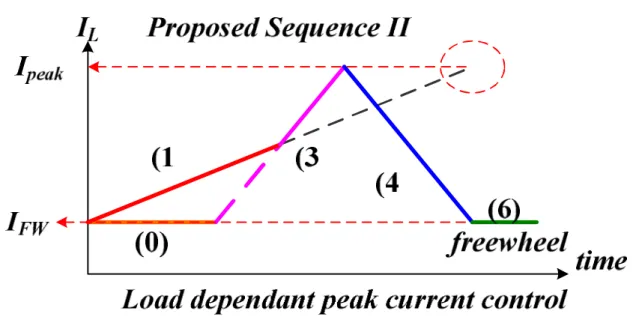
To address these issues, a new proposed controlling sequence-II with the load-dependent
peak-current control (LDPCC) technique is presented as illustrated in Fig. 25. In the
beginning of controlling sequence-II, path 1 is used to simultaneously regulate the buck
output terminal VOA and store the charge with a positive current slope ((VIN-VOA)/L) in the
inductor L, since the voltage level of output terminal VOA is smaller than that of supply
terminal VIN. Path 1 expires; the inductor current (IL) then rapidly increases with a positive
current slope (VIN/L) to the LDPCC level (Ipeak) by path 3. Then controlling sequence-II
((VOB-VIN)/L) to boost the output terminal VOB; after which, it drops back to the inductor
current to a freewheeling current level (IFW). Finally, the inductor current level (IL) is kept by
path 6. Since the current level (Ipeak) increases during heavy load condition and decreases
during light load condition, the power dissipation during the freewheeling loop can be
minimized. Due to the storage charge of the inductor L in path 1 having been fully taken into
account in the proposed controlling sequence-II, the highly undesired current value (IDC1) in
previous work [2] is eliminated. Thus, power conversion efficiency and cross-regulation can
be improved in the proposed controlling sequence-II. However, when the load condition of
output terminals VOA and VOB operate in unbalance output load condition which is the buck
output VOA is derived during heavy load condition and the boost output VOB is derived during
light load condition, the energy still accumulates in the inductor L without releasing path.
Other words, when storage charge during path 1 is higher than releasing charge during path 4,
the value of inductor current level (IL) will not able to decrease inductor current level (IL)
below the LDPCC current level (Ipeak) in every switching cycle. Thus, the inductor current
accumulation appears during unbalance output load condition.
Fig. 25. The proposed sequence-II with LDPCC technique which eliminates the undesired
Fig. 26. The proposed controlling sequence and path 0 of the hysteresis mode control.
In order to address the inductor current (IL) accumulation in the structure of minimum
power switches, a new energy delivering path, which names as path 0 and illustrates in Fig.
26, is proposed to eliminate the energy accumulation issue while the condition that storage
charge during path 1 is higher than consumption charge during path 4. Therefore, a power
comparator is proposed to detect the output load condition. If the output power of output
terminal VOA is smaller than that of output terminal VOB, the proposed controlling sequence-II
is use to regulate voltage level of output terminals. Oppositely, when the output power of
output terminal VOA is larger than that of output terminal VOB, the proposed path 0 is enabled
closed. A current path is created through switches SW4 and SW6 and used to regulate output
terminal VOA. Since the path 0 passes inductor L, the voltage of output VOA is regulated by a
hysteresis voltage window. Therefore, the proposed path 0 also calls as hysteresis mode
control. Since the proposed hysteresis mode control is used to regulate voltage level of output
VOA and to limit regulating ripple of output VOA, the inductor current waveform (IL) which
operates in hysteresis mode is shown in Fig. 25. At the beginning of every switching cycle,
hysteresis mode is enabled. Since inductor current (IL) flows through switches SW4 and SW6 to
output terminal VOA, the energy does not accumulate in the inductor L. Thus, inductor current
level (IL) does not increase until path 0 expires. The duration of path 0 is determined by
hysteresis voltage window and the on-resistance of switches SW4 and SW6. Then, path 3 turns
on, switches SW4 and SW6 is opened, and switch SW3 is closed. The inductor current (IL) is
increased with a positive current slope (VIN/L). When inductor current (IL) raises to LDPCC
level (Ipeak), path 3 expires and then switch SW3 turns off. Then, path 4 and switch SW5 turns
on, the storage charge, in form of inductor current (IL), ramp down with a negative current
slope ((VOB-VIN)/L), the duration of path 4 is determined by the amount of delivering charge.
Finally, the residue current level (IFW) is held by path 6. Owing to the output voltage of output
terminal VOA is regulated by a hysteresis voltage window during path 0, the special operation
which is named as hysteresis control mode caused a larger output ripple and sacrificed power
conversion efficiency in the proposed path 0. However, as the analysis of the hysteresis
control mode, the energy accumulation and cross-regulation during the unbalanced load
condition can be eliminate through path 0.
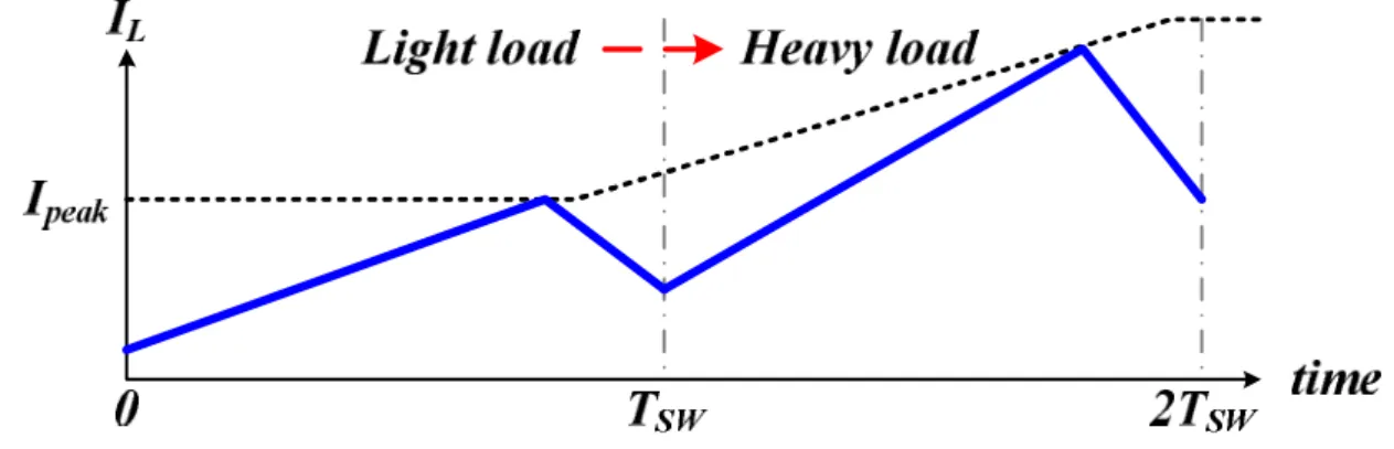
2.2 LDPCC Method for Improving Light-Load
Efficiency, Stability, and Cross-Regulation
Four inductor waveforms are depicted in Fig. 27~30. At first, the inductor current waveform
(IL) of DCM is shown in Fig. 27. The characteristic of inductor current (IL) is that current
level decreases to zero before the end of each switching cycle. The order of the system is
equal to one. That is, only one low-frequency pole exists in the close loop. When load current
changes from light to heavy load condition, the peak value of inductor current (IL) is increased
for storage more energy. There is a maximum peak current level existed, because of the
disappearance of zero-current condition and thus a maximum power limitation exists in the
operation of DCM. As a result, the characteristic of inductor current waveform (IL) changes
from DCM to CCM operation as shown in Fig. 28 when the sudden power is larger than
maximum power limitation of DCM operation. The order of system becomes two and the
Fig. 27. The inductor current waveform in DCM operation when the load current changes
from light to heavy load conduction.
Fig. 28. The inductor current waveform in CCM operation when the load current changes
compensation of system needs a complicated compensation like proportional integral
differential (PID) compensator to make sure large low-frequency gain and suitable phase
margin. Another serious problem is disappearance of isolation period which is zero-current
stage works as freewheeling stage. Since disappearance of isolation period may cause worse
cross regulation. The cross regulation and instability of system comes from the charge
accumulation of inductor. A summary of the two operation modes is that disadvantage of the
DCM operation is maximum power limitation while the disadvantage of CCM operation is
charge accumulation of inductor L.
The PCCM operation was proposed to improve the disadvantages in DCM and CCM
operation [10]. The PCCM technique sets a constant inductor current DC level to store
enough energy in inductor as depicted in Fig. 29. Thus, the order of system is similar to that
of DCM operation while the maximum power delivered by PCCM operation is larger than
that of DCM operation. That is, the order of system is one, and thereby simplifying
compensation skill. After the usage of P-I compensator, bandwidth can be extended to have
better performance for transient response. Nevertheless, the advantages of the PCCM
operation only exist when freewheeling stage exists at end of each switching cycle. Once
disappearance of freewheeling stage happens when load current exceeds maximum power
limitation or when sudden load current changes from light to heavy load level, the stability
and minimized cross regulation isn’t guaranteed since the order of system becomes two. The
solution of scenario is that pre-defined and fixed inductor current level (IDC) is required large
enough to provide maximum power to all output terminals. That is, the value of the
pre-defined and fixed inductor current level (IDC) causes the power conversion lower than that
by CCM or DCM operation at light load condition since the freewheeling stage with high
inductor current occupies the most period of switching cycle. Thus, the light-load efficiency is
decreased. As well, the power conversion efficiency at light-load determines usage time of
Fig. 29. The inductor current waveform in PCCM operation of work [2] when the load
current changes from light to heavy load conduction.
Fig. 30. The inductor current waveform in proposed LDPCC technique operation when the
load current changes from light to heavy load conduction.
To enhance the power conversion efficiency at light-load becomes most important issue
in today’s portable devices. The LDPCC technique is needed to effectively improve the power
conversion efficiency at light-load condition. As illustrated in Fig. 30, the LDPCC technique
is proposed to adaptively store suitable energy in inductor L. When load current changes from
light to heavy load condition, the LDPCC current level (Ipeak) is raised to a higher current
level to store enough charge in inductor L. On other hand, when the load current becomes
small, the LDPCC current level (Ipeak) will be decreased to a small current level for ensuring
high power conversion efficiency at light load condition. Besides, a minimum inductor
current level (IDC(min)) is defined to prevent output terminal from large transient drop voltage.
![Fig. 11. The architecture of dual output DCM converter with TM control method [3].](https://thumb-ap.123doks.com/thumbv2/9libinfo/8762091.208425/33.892.152.779.836.1089/fig-architecture-dual-output-dcm-converter-control-method.webp)
![Fig. 13. The architecture of PCCM control mode for SIDO converter which [10].](https://thumb-ap.123doks.com/thumbv2/9libinfo/8762091.208425/34.892.159.774.764.1087/fig-architecture-pccm-control-mode-sido-converter.webp)
![Fig. 20. The behavior of conventional SIDO converter with one buck and one boost output in [2, and 12]](https://thumb-ap.123doks.com/thumbv2/9libinfo/8762091.208425/44.892.156.785.578.1079/fig-behavior-conventional-sido-converter-buck-boost-output.webp)