國
立
交
通
大
學
材料科學與工程學系
博 士 論
文
藉鎳捉聚改善鎳金屬誘發側向結晶之低溫複晶矽薄膜及奈
米通道電晶體效能研究
Improved Performance of NILC LTPS Thin-Film & Nanowire
Transistors through Ni-Gettering
研 究 生:王寶明
指導教授:吳耀銓 教授
中 華 民 國 九 十 九 年 二 月
藉鎳捉聚改善鎳金屬誘發側向結晶之低溫複晶矽薄膜及奈
米通道電晶體效能研究
Improved Performance of NILC LTPS Thin-Film & Nanowire
Transistors through Ni-Gettering
研 究 生 : 王寶明 Student: Bau-Ming Wang
指導教授 : 吳耀銓 博士 Advisor: Dr. YewChung Sermon Wu
國 立 交 通 大 學
材 料 科 學 與 工 程 學 系
博 士 論 文
A Thesis
Submitted to Department of Materials Science and Engineering College of Engineering
National Chiao Tung University in partial Fulfillment of the Requirements
for the Degree of Doctor of Philosophy in Materials Science and Engineering in
February 2010
Hsinchu, Taiwan, Republic of China
藉鎳捉聚改善鎳金屬誘發側向結晶之低溫複晶矽薄
膜及奈米通道電晶體效能研究
學生:王寶明 指導教授:吳耀銓 博士
國立交通大學材料科學與工程研究所
摘要
本論文主要研究鎳金屬誘發側向結晶(NILC)低溫複晶矽(LTPS)薄膜電晶體(TFTs)。其 中,鎳金屬誘發複晶矽薄膜有鎳金屬殘留的問題,因此發展出有效的鎳金屬捉聚 (Ni‐gettering)方法來降低鎳金屬誘發複晶矽薄膜中的鎳金屬殘留,論文中所提出的鎳金 屬捉聚結構為鎳金屬捉聚層/蝕刻停止層。鎳金屬捉聚層採用非晶矽薄膜及磷佈植非晶 矽薄膜二種,厚度為 100 nm。蝕刻停止層為化學法製備之二氧化矽(Chemical oxide, chem‐SiO2),厚度約 5 nm。論文最後應用此鎳金屬捉聚法於鎳金屬誘發側向結晶複晶矽 薄膜電晶體及矽奈米線通道電晶體(Si NW channel transistors)製作上,以探討鎳金屬對元 件特性的影響。 首先,利用非晶矽薄膜及化學法製備之二氧化矽作為鎳金屬捉聚基版,成功將複晶 矽中殘餘鎳捕捉至鎳金屬捉聚基板中。由 SEM 分析可發現鎳金屬捉聚後聚集在兩相鄰 鎳金屬誘發側向結晶晶界(NILC/NILC boundary)的 NiSi2 蝕刻孔洞明顯減少。此種捉聚方式,是藉由濃度梯度的擴散使得複晶矽中殘餘鎳金屬能成功的透過蝕刻停止層捕捉至上 層鎳金屬捉聚層,因此可發現上層非晶矽由於鎳金屬的擴散而成長出鎳金屬誘發側向結 晶複晶矽。此方法與先前實驗室使用之非晶矽薄膜/電漿輔助化學沈積之氮化矽比較, 可大大降低鎳金屬捉聚時間。其主要原因為鎳原子在氮化矽的擴散速度慢但通過化學氧 化層卻速度快。 除此之外,為提高非晶矽薄膜之鎳金屬捉聚效率。進一步使用離子佈植法將磷雜質 (Phosphorus dopant)佈植於非晶矽薄膜中,成功提高捉聚層之鎳金屬溶解度。由 SEM 分 析可發現鎳金屬捉聚後聚集在兩相鄰鎳金屬誘發側向結晶晶界的 NiSi2 蝕刻孔洞幾乎不 存在。磷離子佈植法雖可以提升鎳金屬捉聚效率,但其佈植濃度在 1x1016 cm‐2才有明顯 效果。且由 SIMS 分析結果發現鎳在捉聚層的分佈與磷佈植曲線相當一致。 將鎳金屬捉聚法應用在鎳金屬誘發側向結晶複晶矽薄膜電晶體製備上,從元件特性 得知,鎳金屬誘發側向結晶複晶矽薄膜電晶體在經過鎳捉聚處理後,可獲得較佳的電特 性及均勻性,如降低漏電流(Leakage current)及抑制臨界電壓(Threshold voltage)負偏移 等,其主要原因為鎳金屬誘發側向結晶複晶矽薄膜之鎳金屬殘留量可有效降低。
最後利用一個簡單及低成本的方法去製作矽奈米線通道電晶體。其製備之特點為利 用一般製作 MOSFET 元件的側壁邊襯(Sidewall spacer)之概念,以底閘極薄膜電晶體結構 在定義汲極和源極之同時,可自我對準形成奈米線通道。此複晶矽邊襯奈米線縱剖面近 似三角形,其寬度及厚度可以控制至 70 nm。此奈米線通道薄膜電晶體比一般傳統薄膜
電晶體有比較好的通道控制能力。且經由鎳金屬捉聚處理後,鎳金屬誘發側向結晶複晶 矽奈米線通道電晶體在電性與均勻性上獲得提升。主要原因為多晶矽邊襯奈米線通道內 及其與氧化層之介面鎳金屬殘留量減少。
關鍵字:鎳捉聚、化學氧化層、磷雜質、鎳金屬誘發側向結晶、低溫複晶矽、奈米線、 薄膜電晶體、矽奈米通道電晶體、側壁邊襯、漏電流
Improved Performance of NILC LTPS Thin-Film &
Nanowire Transistors through Ni-Gettering
Student: Bau-Ming Wang Advisor: Dr. YewChung Sermon Wu
Department of Materials Science and Engineering
National Chiao Tung University
Abstract
Low temperature polycrystalline silicon (LTPS) Ni‐metal induced lateral crystallization (NILC) thin‐film transistors (TFTs) have been investigated in this thesis. Ni impurities trapped inside the NILC poly‐Si films is an issue. Therefore the Ni‐gettering method is proposed to effectively reduce Ni residues within the NILC poly‐Si films. It involves using gettering layers/etching stop layers as the Ni‐gettering structure. The 100‐nm‐thick top α‐Si and phosphorous‐doped α‐Si layers serve as the gettering layers, while the middle ~5‐nm‐thick chem‐SiO2 layer is used as an etching stop layer. Moreover the proposed gettering method is utilized in the fabrication of LTPS NILC TFTs and Si nanowire (NW) channel transistors to investigate the effect of Ni‐metal inside poly‐Si on the device performance.
reduction is demonstrated by SEM. After the gettering process, fewer and smaller silicide‐etching holes are found at the NILC/NILC boundaries. It is found that top α‐Si films, Ni‐gettering layers, transfer into NILC poly‐Si verified by SEM. This means that during the gettering process, Ni atoms diffused from the NILC poly‐Si film through chem‐SiO2 into the Ni‐gettering layer due to the concentration gradient. Compared with the previous α‐Si/PECVD‐SiNx study, the thermal budget is greatly reduced. It’s because of low Ni diffusivity in SiNx films resulting a long annealing time as 90 h at 550oC in N2 ambient.
In order to improve the Ni‐gettering efficiency, phosphorous‐doped α‐Si films are further used by ion implantation. After a gettering process, there are almost no silicide‐etching holes observed at the NILC/NILC boundaries. These results indicate that phosphorous dopants could improve the gettering efficiency of α‐Si due to the solubility enhancement of Ni impurities. But the gettering efficiency do not obviously improves until doping phosphorus ions reach a dose of 1×1016 cm‐2. The concentration distribution of Ni is similar to that of phosphorous atoms since the projection range of phosphorous ions is set at the middle of the α‐Si film. This result also indicates that phosphorus could trap Ni atoms.
The proposed gettering method is further utilized in the fabrication of LTPS NILC TFTs. As NILC TFTs are treated with a Ni‐gettering process, they reveal lower leakage current, higher on/off current ratio, higher mobility, and better uniformity. These improvements are
all attributed to the reduction of Ni impurities in gettered poly‐Si films.
Finally, a simple method and low‐cost process is used to manufacture the NW channels. The feature of process is the method of forming sidewall spacer of MOSFET. The poly‐Si sidewall spacer NW channels self‐alignment form in the process of defining source/drain (S/D). Both the vertical width (WNW) and the horizontal sidewall thickness (TNW) of poly‐Si NWs are about 70 nm. The cross‐section of fabricated poly‐Si NWs is similar to triangular shape by an anisotropic etching. Compared with the traditional TFTs, the side‐gated NWs TFTs have higher channel controllability. Moreover, the performance of NILC NWs TFTs is improved after a Ni‐gettering process. This is because of the reduction of Ni and NiSi2 precipitates randomly trapped at poly‐Si/gate oxide interfaces and poly‐Si grain boundaries.
Keywords: Ni‐Gettering, Chemical Oxide (chem‐SiO2), Phosphorus Dopant, Nickel‐Metal Induced Lateral Crystallization (NILC), Low Temperature Polycrystalline Silicon (LTPS), Nanowire (NW), Thin‐Film Transistors (TFTs), Si Nanowire Channel Transistors, Sidewall Spacer, Leakage Current
誌謝
感謝指導教授吳耀銓博士在我博士生涯後半段給予辛勤的指導與提攜,在生活上及 論文研究上給予關懷及協助。也感謝涂肇嘉博士及蔡明蒔博士在碩士班期間及博士生涯 前半段的指導。另外感謝口試委員交通大學材料所陳智博士、吳文偉博士與隆達電子副 理趙志偉博士、工研院顯示所胡國仁博士,在博士論文口試時,對論文研究給予意見與 指導,讓本論文更加完備。 其次感謝交通大學奈米元件中心、國家奈米元件實驗室在實驗設備上的支持及協 助。此外感謝國家奈米元件實驗室李美儀小姐、賴東彥先生、楊子明先生、吳鴻佑先生、 孫旭昌先生、許倬綸先生、趙國芬小姐、賴明志先生、楊忠諺博士及蘇旺申博士等人在 研究上的協助。也要感謝交通大學奈米元件中心何惟梅小姐、徐綉鑾小姐、范秀蘭小姐、 蘇俊榮博士的幫助,讓我在奈米中心的實驗能順利完成。 由衷感謝實驗室的趙志偉學長、胡國仁學長、侯智元學長、胡晟民、施協志、廖崢、 汪砡華、張志榜、鄭季豪、黃秉緯、林博文、林其慶、吳騏廷、賴明輝、陳建誌、謝承 佑、邱偉哲、陳亦宏、陳俞中、張勝傑、張岱民、曾卿杰、黃璽豪、趙育誠、廖偉志、 鄭筑文、童騰賦、許育程、鍾承璋、錢奐宇、卓昕如、鄭文豪、邱郁珈、牛振儀,有你 們的協助,我才能順利完成博士學位。最後感謝陪伴我渡過博士生涯的好伙伴們林勝 結、謝逸凡、徐繹翔、魏伸紘、王馨瑩、張智傑、李建財,由於各位的支持與關懷,讓 我的博士生涯過的多采多姿。 僅此論文獻給我的家人,感謝他們在我求學期間給予無私的包容與支持,讓我在研 究上能無後顧之憂。 2010 年 2 月于新竹交大Contents
Abstract (Chinese) ... I Abstract (English) ... IV Acknowledgment (Chinese) ... VII Contents ... VIII Figure Captions ... XI Table Lists ... XVI Chapter 1 Introduction ... 1 1.1 An Overview of Polycrystalline Silicon Thin‐Film Transistors (TFTs) ... 2 1.2 Low‐Temperature Polycrystalline Silicon (LTPS) Crystallization... 4 1.2.1 Solid‐Phase Crystallization (SPC) ... 4 1.2.2 Metal‐Mediated Induced Crystallization ... 5 1.3 Metal Gettering from Silicon ... 12 1.4 Silicon Nanowires (NWs) Fabrication ... 17 1.4.1 Top‐Down Method ... 17 1.4.2 Bottom‐Up Method ... 18 1.5 Motivation and Thesis Organization ... 19Chapter 2 Ni Reduction of Nickel‐Mediated Crystallization Polycrystalline Silicon Using A Ni‐Gettering Process ... 23
2.1 Introduction ... 23 2.2 Experimental Procedure ... 24 2.2.1 Gettering of Ni Residues from NILC Poly‐Si Films ... 24 2.2.2 Gettering of Ni Residues from NIC Poly‐Si Films ... 26 2.2.3 Dopant Effect on NILC Rate ... 29 2.3 Results and Discussion ... 30 2.3.1 Characterization of NILC Poly‐Si Films ... 30 2.3.2 Quality of chem‐SiO2 Layers ... 30 2.3.3 Ni‐Gettering Using chem‐SiO2 Interlayer ... 35 2.3.4 Improved Ni‐Gettering Efficiency by Phosphorus Ions Implant ... 38 2.3.5 Effect of Phosphorus Ions and Implant Damages on NILC Rate ... 47 2.4 Summary ... 48
Chapter 3 Using Phosphorous‐Doped α‐Si Gettering Layer to Improve NILC Poly‐Si TFTs Performance ... 52 3.1 Introduction ... 52 3.2 Device Fabrication ... 53 3.3 Results and Discussion ... 56 3.3.1 Ni‐Gettering Phenomenon ... 56 3.3.2 Basic Electrical Characteristics of Poly‐Si TFTs ... 59 3.3.3 Improved Uniformity of NILC Poly‐Si TFTs by Ni‐Gettering ... 66 3.4 Summary ... 66 Chapter 4 Improved Performance and Uniformity of NILC Poly‐Si Nanowires TFTs through Ni‐Gettering ... 70 4.1 Introduction ... 70
4.2 Device Fabrication ... 71 4.3 Results and Discussion ... 77 4.3.1 Characterization of Fabricated Poly‐Si NWs ... 77 4.3.2 Device Performances of Poly‐Si NWs TFTs ... 77 4.3.3 Uniformity Improved in Poly‐Si NWs TFTs by Ni‐Gettering ... 83 4.4 Summary ... 87 Chapter 5 Conclusions and Future Work ... 88 5.1 Conclusions ... 88 5.2 Future Work ... 90 References ... 92 Vita ... 104 Publication List ... 105
Figure Captions
Figure 1‐1 The device structure of a top‐gated thin‐film transistor (TFT). ‐‐‐‐‐‐‐‐‐‐‐‐‐‐‐‐‐‐‐‐‐‐‐‐‐‐ 3 Figure 1‐2 The crystalline structures: (a) the diamond structure of Si and (b) the fluorite
structure NiSi2. ‐‐‐‐‐‐‐‐‐‐‐‐‐‐‐‐‐‐‐‐‐‐‐‐‐‐‐‐‐‐‐‐‐‐‐‐‐‐‐‐‐‐‐‐‐‐‐‐‐‐‐‐‐‐‐‐‐‐‐‐‐‐‐‐‐‐‐‐‐‐‐‐‐‐‐‐‐‐‐‐‐‐‐‐‐‐‐‐‐‐ 7 Figure 1‐3 The formation temperature map of thin‐film Ni silicides on (a) α‐Si, and (b) c‐Si
[44]. ‐‐‐‐‐‐‐‐‐‐‐‐‐‐‐‐‐‐‐‐‐‐‐‐‐‐‐‐‐‐‐‐‐‐‐‐‐‐‐‐‐‐‐‐‐‐‐‐‐‐‐‐‐‐‐‐‐‐‐‐‐‐‐‐‐‐‐‐‐‐‐‐‐‐‐‐‐‐‐‐‐‐‐‐‐‐‐‐‐‐‐‐‐‐‐‐‐‐‐‐‐‐‐‐ 8 Figure 1‐4 The equilibrium molar free‐energy diagram for NiSi2 in contact with α‐Si and c‐Si [38]. ‐‐‐‐‐‐‐‐‐‐‐‐‐‐‐‐‐‐‐‐‐‐‐‐‐‐‐‐‐‐‐‐‐‐‐‐‐‐‐‐‐‐‐‐‐‐‐‐‐‐‐‐‐‐‐‐‐‐‐‐‐‐‐‐‐‐‐‐‐‐‐‐‐‐‐‐‐‐‐‐‐‐‐‐‐‐‐‐‐‐‐‐‐‐‐‐‐‐‐‐‐‐‐‐ 9 Figure 1‐5 A possible modification of the c‐Si growth mechanism involving the formation of a thin layer of c‐Si at the α‐Si/NiSi2 interface [38]. ‐‐‐‐‐‐‐‐‐‐‐‐‐‐‐‐‐‐‐‐‐‐‐‐‐‐‐‐‐‐‐‐‐‐‐‐‐‐‐‐‐‐‐‐‐‐‐ 11 Figure 1‐6 The concept of the gettering process including release, diffusion, and capture of the metal impurities [47]. ‐‐‐‐‐‐‐‐‐‐‐‐‐‐‐‐‐‐‐‐‐‐‐‐‐‐‐‐‐‐‐‐‐‐‐‐‐‐‐‐‐‐‐‐‐‐‐‐‐‐‐‐‐‐‐‐‐‐‐‐‐‐‐‐‐‐‐‐‐‐‐‐‐‐‐‐ 13 Figure 1‐7 (a) A gettering structure with a Ni gettering layer and an etching stop layer, and (b) the device region protected well by an etching stop layer during the removal of the Ni gettering layer. ‐‐‐‐‐‐‐‐‐‐‐‐‐‐‐‐‐‐‐‐‐‐‐‐‐‐‐‐‐‐‐‐‐‐‐‐‐‐‐‐‐‐‐‐‐‐‐‐‐‐‐‐‐‐‐‐‐‐‐‐‐‐‐‐‐‐‐‐‐‐‐‐‐‐‐‐‐‐‐‐‐‐‐‐‐‐‐‐‐‐ 16 Figure 1‐8 (a) Photoresist patterns on top of the poly‐Si surface by the conventional
lithography, and (b) the sidewall spacer NW channels fabricated by an anisotropic etching. ‐‐‐‐‐‐‐‐‐‐‐‐‐‐‐‐‐‐‐‐‐‐‐‐‐‐‐‐‐‐‐‐‐‐‐‐‐‐‐‐‐‐‐‐‐‐‐‐‐‐‐‐‐‐‐‐‐‐‐‐‐‐‐‐‐‐‐‐‐‐‐‐‐‐‐‐‐‐‐‐‐‐‐‐‐‐‐‐‐‐‐‐‐‐‐‐‐‐‐ 20 Figure 2‐1 Schematic illustration of the Ni‐gettering process: (a) fabrication of the NILC
poly‐Si film, (b) removal of unreacted Ni pads, (c) capped with an etching stop layer (chem‐SiO2) and a gettering layer (α‐Si or p‐α‐Si), and (d) removal of the gettering layer and the chem‐SiO2 layer. ‐‐‐‐‐‐‐‐‐‐‐‐‐‐‐‐‐‐‐‐‐‐‐‐‐‐‐‐‐‐‐‐‐‐‐‐‐‐‐‐‐‐‐‐‐‐‐‐‐‐‐‐‐‐‐‐‐‐‐‐‐‐‐‐‐‐‐‐‐‐ 25
Figure 2‐2 Schematic illustration of the Ni‐gettering process of the NIC poly‐Si: (a) fabrication of the NIC poly‐Si film (b) removal of unreacted Ni films, and (c) capped with a chem‐SiO2 layer and a gettering layer (α‐Si or p‐α‐Si). ‐‐‐‐‐‐‐‐‐‐‐‐‐‐‐‐‐‐‐‐‐‐‐‐‐‐‐‐‐‐‐‐‐‐‐‐‐‐‐ 28 Figure 2‐3 OM image of the α‐Si film after a NILC process carried out at 540oC for 24 h in N2
ambient.‐‐‐‐‐‐‐‐‐‐‐‐‐‐‐‐‐‐‐‐‐‐‐‐‐‐‐‐‐‐‐‐‐‐‐‐‐‐‐‐‐‐‐‐‐‐‐‐‐‐‐‐‐‐‐‐‐‐‐‐‐‐‐‐‐‐‐‐‐‐‐‐‐‐‐‐‐‐‐‐‐‐‐‐‐‐‐‐‐‐‐‐‐‐‐‐‐‐ 31 Figure 2‐4 The dependence of the NILC length on the anneal time. The NILC was carried out
at 540oC in N2 ambient. ‐‐‐‐‐‐‐‐‐‐‐‐‐‐‐‐‐‐‐‐‐‐‐‐‐‐‐‐‐‐‐‐‐‐‐‐‐‐‐‐‐‐‐‐‐‐‐‐‐‐‐‐‐‐‐‐‐‐‐‐‐‐‐‐‐‐‐‐‐‐‐‐‐‐‐‐‐‐ 32 Figure 2‐5 SEM image of the NILC poly‐Si grains treated with Secco‐etching.‐‐‐‐‐‐‐‐‐‐‐‐‐‐‐‐‐‐‐‐ 33 Figure 2‐6 (a) Cross‐sectional TEM images of the NILC Poly‐Si films capped with the chemical
oxide films, and (b) the high magnification of a chemical oxide film around 5 nm thick. Platinum (Pt) films were deposited on top of the chem‐SiO2 layers for image contrast. ‐‐‐‐‐‐‐‐‐‐‐‐‐‐‐‐‐‐‐‐‐‐‐‐‐‐‐‐‐‐‐‐‐‐‐‐‐‐‐‐‐‐‐‐‐‐‐‐‐‐‐‐‐‐‐‐‐‐‐‐‐‐‐‐‐‐‐‐‐‐‐‐‐‐‐‐‐‐‐‐‐‐‐‐‐‐‐‐‐‐‐‐‐‐‐‐‐‐‐‐‐‐‐‐‐‐‐‐‐ 34 Figure 2‐7 AFM images of the NILC poly‐Si surfaces (a) without Ni‐gettering, and with
Ni‐gettering by (b) a α‐Si layer, and (c) a p‐α‐Si layer (the dosage was 1×1016 cm‐2). ‐ 36 Figure 2‐8 OM images of the Ni‐gettering layers: (a) a α‐Si film deposited on a chem‐SiO2
layer by LPCVD and then phosphorous ions implanted at a dosage of (b) 1×1014 cm‐2, (c) 1×1015 cm‐2, and (d) 1×1016 cm‐2, respectively. ‐‐‐‐‐‐‐‐‐‐‐‐‐‐‐‐‐‐‐‐‐‐‐‐‐‐‐‐‐‐‐‐‐‐‐‐‐‐‐‐‐‐‐‐‐ 37 Figure 2‐9 OM images of the Ni‐gettering phenomenon by (a) a α‐Si film, and the
phosphorous‐doped α‐Si films at a dosage of (b) 1×1014 cm‐2, (c) 1×1015 cm‐2, and (d) 1×1016 cm‐2, respectively. ‐‐‐‐‐‐‐‐‐‐‐‐‐‐‐‐‐‐‐‐‐‐‐‐‐‐‐‐‐‐‐‐‐‐‐‐‐‐‐‐‐‐‐‐‐‐‐‐‐‐‐‐‐‐‐‐‐‐‐‐‐‐‐‐‐‐‐‐‐‐‐‐‐‐‐‐ 39 Figure 2‐10 SEM images of the NILC poly‐Si grains of Ni‐gettering layers: (a) a α‐Si film, and (b)
a phosphorous‐doped α‐Si film at a dosage of 1×1016 cm‐2. Samples were treated with Secco‐etching. ‐‐‐‐‐‐‐‐‐‐‐‐‐‐‐‐‐‐‐‐‐‐‐‐‐‐‐‐‐‐‐‐‐‐‐‐‐‐‐‐‐‐‐‐‐‐‐‐‐‐‐‐‐‐‐‐‐‐‐‐‐‐‐‐‐‐‐‐‐‐‐‐‐‐‐‐‐‐‐‐‐‐‐‐ 40 Figure 2‐11 OM image of NILC/NILC boundary treated with TMAH etching. ‐‐‐‐‐‐‐‐‐‐‐‐‐‐‐‐‐‐‐‐‐ 42 Figure 2‐12 Schematic illustration of (a) silicide‐etching holes at NILC/NILC boundaries, and
SEM images of etching holes of (b) NoGET, (c) ASiGET, (d) PSiGET‐14, (e) PSiGET‐15, and (f) PSiGET‐16. Samples were treated with the silicide‐etching solution. ‐‐‐‐‐‐‐‐‐ 43 Figure 2‐13 (a) Cross‐sectional TEM images of NIC Poly‐Si films capped with chemical oxide
films and gettering layers, and (b) the high magnification of a gettering layer around 110 nm thick. The gettering layer was implanted with 1×1016 cm‐2 phosphorous ions and the projection range (Rp) was about 50 nm in depth. ‐‐‐‐‐‐‐‐‐‐‐‐‐‐‐‐‐‐‐‐‐‐‐‐‐‐‐‐‐‐‐‐‐‐ 45 Figure 2‐14 SIMS depth profiles of NIC poly‐Si films treated with and without a Ni‐gettering process. ‐‐‐‐‐‐‐‐‐‐‐‐‐‐‐‐‐‐‐‐‐‐‐‐‐‐‐‐‐‐‐‐‐‐‐‐‐‐‐‐‐‐‐‐‐‐‐‐‐‐‐‐‐‐‐‐‐‐‐‐‐‐‐‐‐‐‐‐‐‐‐‐‐‐‐‐‐‐‐‐‐‐‐‐‐‐‐‐‐‐‐‐‐‐‐‐‐‐‐ 46 Figure 2‐15 NILC length vs. anneal time and different doping type. NILC was carried out at 540oC in N2 ambient. ‐‐‐‐‐‐‐‐‐‐‐‐‐‐‐‐‐‐‐‐‐‐‐‐‐‐‐‐‐‐‐‐‐‐‐‐‐‐‐‐‐‐‐‐‐‐‐‐‐‐‐‐‐‐‐‐‐‐‐‐‐‐‐‐‐‐‐‐‐‐‐‐‐‐‐‐‐‐‐‐‐‐ 49 Figure 2‐16 NILC length vs. different doping type and dose after heat treatment at 540oC for 16 h in N2 ambient. ‐‐‐‐‐‐‐‐‐‐‐‐‐‐‐‐‐‐‐‐‐‐‐‐‐‐‐‐‐‐‐‐‐‐‐‐‐‐‐‐‐‐‐‐‐‐‐‐‐‐‐‐‐‐‐‐‐‐‐‐‐‐‐‐‐‐‐‐‐‐‐‐‐‐‐‐‐‐‐‐‐‐‐‐ 50 Figure 3‐1 Schematic illustration of the TFTs device fabrication: (a) the top view of the
fabricated device, (b) fabrication of NILC‐Si, (c) capped with an etching stop layer (chem‐SiO2) and a gettering layer (p‐α‐Si), (d) removal of the gettering layer and chem‐SiO2 layer, (e) capped with a low‐temperature oxide (LTO) as gate‐oxide and a α‐Si film as gate material, and (f) capped with a LTO as the isolation layer and fabrication of Al electrodes. ‐‐‐‐‐‐‐‐‐‐‐‐‐‐‐‐‐‐‐‐‐‐‐‐‐‐‐‐‐‐‐‐‐‐‐‐‐‐‐‐‐‐‐‐‐‐‐‐‐‐‐‐‐‐‐‐‐‐‐‐‐‐‐‐‐‐‐‐‐‐‐‐‐ 54 Figure 3‐2 (a) OM image of the α‐Si film after a NILC process carried out at 540oC for 24 h in N2 ambient, and (b) SEM image of the NILC poly‐Si grains treated with Secco‐etching. ‐‐‐‐‐‐‐‐‐‐‐‐‐‐‐‐‐‐‐‐‐‐‐‐‐‐‐‐‐‐‐‐‐‐‐‐‐‐‐‐‐‐‐‐‐‐‐‐‐‐‐‐‐‐‐‐‐‐‐‐‐‐‐‐‐‐‐‐‐‐‐‐‐‐‐‐‐‐‐‐‐‐‐‐‐‐‐‐‐‐‐‐‐‐‐‐‐‐‐‐‐‐‐‐‐‐‐‐‐ 57 Figure 3‐3 OM images of (a) a Ni‐gettering layer, α‐Si film, deposited on a chem‐SiO2 layer by LPCVD, and (b) the Ni‐gettering phenomenon by a phosphorous‐doped α‐Si film at a dosage of 1×1016 cm‐2. ‐‐‐‐‐‐‐‐‐‐‐‐‐‐‐‐‐‐‐‐‐‐‐‐‐‐‐‐‐‐‐‐‐‐‐‐‐‐‐‐‐‐‐‐‐‐‐‐‐‐‐‐‐‐‐‐‐‐‐‐‐‐‐‐‐‐‐‐‐‐‐‐‐‐‐‐‐‐‐‐ 58 Figure 3‐4 Schematic illustration of (a) silicide‐etched holes at NILC/NILC boundaries, and
were treated with the silicide‐etching solution. ‐‐‐‐‐‐‐‐‐‐‐‐‐‐‐‐‐‐‐‐‐‐‐‐‐‐‐‐‐‐‐‐‐‐‐‐‐‐‐‐‐‐‐‐‐‐‐ 60 Figure 3‐5 Typical ID‐VG transfer curves of the NILC TFT and the GETR TFT measured at VD = 5
V and VD = 0.1 V, respectively. ‐‐‐‐‐‐‐‐‐‐‐‐‐‐‐‐‐‐‐‐‐‐‐‐‐‐‐‐‐‐‐‐‐‐‐‐‐‐‐‐‐‐‐‐‐‐‐‐‐‐‐‐‐‐‐‐‐‐‐‐‐‐‐‐‐‐‐‐‐‐ 61 Figure 3‐6 (a) △VTH and IOFF_min were measured in ten NILC TFTs to investigate the
device‐to‐device variation, and (b) the ID‐VG transfer curves of ten NILC TFTs measured at VD = 5 V and VD = 0.1 V, respectively. ‐‐‐‐‐‐‐‐‐‐‐‐‐‐‐‐‐‐‐‐‐‐‐‐‐‐‐‐‐‐‐‐‐‐‐‐‐‐‐‐‐‐‐‐ 67 Figure 3‐7 (a) △VTH and IOFF_min were measured in ten GETR TFTs to investigate the
device‐to‐device variation, and (b) the ID‐VG transfer curves of ten GETR TFTs measured at VD = 5 V and VD = 0.1 V, respectively. ‐‐‐‐‐‐‐‐‐‐‐‐‐‐‐‐‐‐‐‐‐‐‐‐‐‐‐‐‐‐‐‐‐‐‐‐‐‐‐‐‐‐‐‐ 68 Figure 4‐1 (a) Cross‐sectional SEM image of a 100‐nm‐thick LPCVD α‐Si film capped on a
40‐nm‐thick TEOS oxide, and (b) OM image of a 4x4 μm Ni pad on a α‐Si film before basic NILC process. ‐‐‐‐‐‐‐‐‐‐‐‐‐‐‐‐‐‐‐‐‐‐‐‐‐‐‐‐‐‐‐‐‐‐‐‐‐‐‐‐‐‐‐‐‐‐‐‐‐‐‐‐‐‐‐‐‐‐‐‐‐‐‐‐‐‐‐‐‐‐‐‐‐‐‐‐‐‐‐‐‐‐‐‐ 72 Figure 4‐2 (a) OM image of NILC poly‐Si after annealing at 540oC for 24 h in N2 ambient, (b)
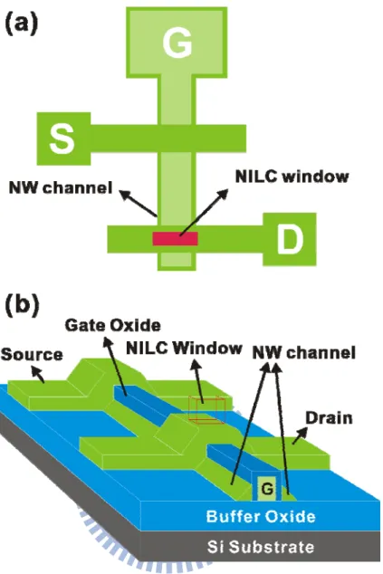
the cross‐sectional view along the dashed line A to B in Fig. 4‐2a, and (c) the Ni‐gettering structure. ‐‐‐‐‐‐‐‐‐‐‐‐‐‐‐‐‐‐‐‐‐‐‐‐‐‐‐‐‐‐‐‐‐‐‐‐‐‐‐‐‐‐‐‐‐‐‐‐‐‐‐‐‐‐‐‐‐‐‐‐‐‐‐‐‐‐‐‐‐‐‐‐‐‐‐‐‐‐‐‐ 74 Figure 4‐3 (a) Top view of the proposed NILC poly‐Si NWs TFT structure, and (b) the 3‐D
schematic of poly‐Si NWs TFTs. ‐‐‐‐‐‐‐‐‐‐‐‐‐‐‐‐‐‐‐‐‐‐‐‐‐‐‐‐‐‐‐‐‐‐‐‐‐‐‐‐‐‐‐‐‐‐‐‐‐‐‐‐‐‐‐‐‐‐‐‐‐‐‐‐‐‐‐‐‐ 75 Figure 4‐4 SEM images of (a) top view and (b) side view of the source/drain (S/D) formation with a couple of poly‐Si NW channels after an anisotropic etching. ‐‐‐‐‐‐‐‐‐‐‐‐‐‐‐‐‐‐‐‐‐‐ 76 Figure 4‐5 (a) Cross‐sectional TEM image of the NILC NWs TFT with a couple of poly‐Si NW channels, and (b) the high magnification of poly‐Si NWs in Fig. 4‐3a. ‐‐‐‐‐‐‐‐‐‐‐‐‐‐‐‐‐‐‐‐ 78 Figure 4‐6 Comparison of transfer characteristics among SPC, NILC, and GETR NWs TFTs. ‐‐‐ 80 Figure 4‐7 Plot of ln(ID/VG‐VFB) versus 1/(VG‐VFB)2 and the extracted trap state density of SPC,
NILC and GETR NWs TFTs. ID was measured at VD = 0.5 V. ‐‐‐‐‐‐‐‐‐‐‐‐‐‐‐‐‐‐‐‐‐‐‐‐‐‐‐‐‐‐‐‐‐ 82 Figure 4‐8 (a) VTH and IOFF were measured in ten SPC NWs TFTs to investigate the
device‐to‐device variation, and typical ID‐VG transfer curves of ten (b) SPC NWs TFTs measured at VD = 3 V and VD = 0.5 V, respectively. ‐‐‐‐‐‐‐‐‐‐‐‐‐‐‐‐‐‐‐‐‐‐‐‐‐‐‐‐‐‐‐‐‐‐‐‐‐‐‐‐‐‐‐‐ 84 Figure 4‐9 (a) VTH and IOFF were measured in ten NILC NWs TFTs to investigate the
device‐to‐device variation, and typical ID‐VG transfer curves of ten (b) NILC NWs TFTs measured at VD = 3 V and VD = 0.5 V, respectively. ‐‐‐‐‐‐‐‐‐‐‐‐‐‐‐‐‐‐‐‐‐‐‐‐‐‐‐‐‐‐‐‐‐‐‐‐‐‐‐‐‐‐‐‐ 85 Figure 4‐10 (a) VTH and IOFF were measured in ten NILC NWs TFTs to investigate the
device‐to‐device variation, and typical ID‐VG transfer curves of ten (b) NILC NWs TFTs measured at VD = 3 V and VD = 0.5 V, respectively. ‐‐‐‐‐‐‐‐‐‐‐‐‐‐‐‐‐‐‐‐‐‐‐‐‐‐‐‐‐‐‐‐‐‐‐‐‐‐‐‐‐‐‐‐ 86
Table Lists
Table 2‐1 Relevant parameters of the Ni‐gettering layers. ‐‐‐‐‐‐‐‐‐‐‐‐‐‐‐‐‐‐‐‐‐‐‐‐‐‐‐‐‐‐‐‐‐‐‐‐‐‐‐‐‐‐‐‐ 27 Table 3‐1 Device characteristics of the NILC TFTs and the GETR TFTs. Data were measured in ten devices, respectively. ‐‐‐‐‐‐‐‐‐‐‐‐‐‐‐‐‐‐‐‐‐‐‐‐‐‐‐‐‐‐‐‐‐‐‐‐‐‐‐‐‐‐‐‐‐‐‐‐‐‐‐‐‐‐‐‐‐‐‐‐‐‐‐‐‐‐‐‐‐‐‐‐‐‐‐‐ 62 Table 4‐1 Device characteristics of NILC, GETR and SPC NWs TFTs. Data were measured in ten devices, respectively. ‐‐‐‐‐‐‐‐‐‐‐‐‐‐‐‐‐‐‐‐‐‐‐‐‐‐‐‐‐‐‐‐‐‐‐‐‐‐‐‐‐‐‐‐‐‐‐‐‐‐‐‐‐‐‐‐‐‐‐‐‐‐‐‐‐‐‐‐‐‐‐‐‐‐‐‐ 81Chapter 1 Introduction
Low‐temperature polycrystalline silicon (LTPS) thin‐film transistors (TFTs) have attracted considerable interest for their use in active‐matrix liquid crystal displays (AMLCDs) [1‐3] and active‐matrix organic light emitting displayers (AMOLEDs) [4‐6] because they exhibit good electrical properties and can be integrated in peripheral circuits on inexpensive glass substrates. Since polycrystalline silicon (poly‐Si) TFTs require glass substrates, intensive studies have been carried out to lower the crystallization temperature of amorphous silicon (α‐Si) films. Ni‐metal induced lateral crystallization (NILC) is one of these efforts. [7‐12] Unfortunately, the NILC poly‐Si grain boundaries trap Ni and NiSi2 precipitates, which increase the leakage current and shift the threshold voltage. [12–16] Therefore, Ni contamination inside the NILC poly‐Si film should be reduced. The goal of this work is to getter nickel impurities within NILC poly‐Si to improve the performance of LTPS NILC TFTs.
In this chapter, an overview of poly‐Si TFTs is first reviewed. Then the processes of low temperature poly‐Si crystallization and the metal gettering from Si are introduced. Finally, the architectures of LTPS NILC nanowires (NWs) for improving the performance of TFTs are discussed, followed with the motivation of this work.
1.1 An Overview of Polycrystalline Silicon Thin-Film Transistors (TFTs)
The α‐Si TFTs as the pixel switching device for active matrix liquid crystal displays (AMLCDs) is the mainstream technology due to low processing temperature (<350oC) compatible with the glass substrate. [17, 18] However the poor field‐effect mobility (typically < 1 cm2/Vs) and the small on‐current in α‐Si TFTs limit themselves as the switching elements only. Therefore, the poly‐Si becomes an attractive candidate for AMLCDs.
In 1980, the high temperature poly‐Si TFTs with electron field‐effect mobility around 50 cm2/Vs were proposed. [19] This technique requires a high strain temperature substrate such as quartz, due to the gate insulator SiO2 grown thermally at 1050oC. Hence several techniques for poly‐Si TFTs fabrication at low temperature (below 600°C) began in 1980s. The low‐cost glass replaced quartz substrate and made high‐definition AMLCD more practical and less expensive. In fact, the field effect mobility in poly‐Si TFTs is significantly higher than that of α‐Si about two orders of magnitudes. [20] The higher drive current allows small TFTs to be used as the pixel switching elements, resulting in higher aperture ratio and lower parasitic gate‐line capacitance for improved display performance. [21]
Device structure of TFTs unlike MOSFETs, the active layer separately forms on the substrate, as shown in Fig 1‐1. The quality of crystallized poly‐Si films is therefore quite sensitive to the performance of poly‐Si TFTs. The crystallized poly‐Si fabricated by various
Figure 1‐1 The device structure of a top‐gated thin‐film transistor (TFT).
techniques at low temperature such as: (1) solid phase crystallization (SPC), (2) Ni‐metal induced lateral crystallization (NILC) will be reviewed in detail.
1.2 Low-Temperature Polycrystalline Silicon (LTPS) Crystallization
The most important step in the fabrication of LTPS TFTs has been considered as the crystallization of α‐Si films. The quality of crystallized poly‐Si films plays an important role on the performance of poly‐Si TFTs. Historically, solid phase crystallization (SPC) [22] is the first technology to produce poly‐Si films for display applications, followed by metal mediated induced crystallization. The ultimate goal of the LTPS technology is to integrate the pixel‐driving circuits on the display substrate. These two low‐temperature poly‐Si crystallization methods are introduced as follows:
1.2.1 Solid-Phase Crystallization (SPC)
Amorphous Si (α‐Si) is a thermodynamically meta‐stable phase. It requires a sufficient energy to overcome the initial energy barrier for transformation to polycrystalline phase. The transformation is carried out by annealing in a furnace at certain temperature (typically at 600oC) for duration time (about 24 h) to break and reorganize Si bonds. Since the solid state still stays during the phase transformation, the technique is called solid‐phase crystallization (SPC). Deposited α‐Si thin films transformed to poly‐Si using SPC method have obtained better TFT device electrical performance than as‐deposited poly‐Si films. [23]
In general, the poly‐Si crystallized from α‐Si usually has larger grain size than that of as‐deposited poly‐Si. Most defects are generated at the grain boundaries in poly‐Si films.
The phase transformation occurs through two processed, the nucleation and grain growth, and both have characteristic activation energies. [24] The nucleation activation energy is normally larger than the grain growth activation energy. [25] To enlarge poly‐Si grains by SPC, it’s necessary to suppress nucleation; therefore SPC is typically carried out at low temperature. Higher disorder structure requires higher energy barrier to form the Si nuclei. [26, 27] Hence SPC poly‐Si grain size could be controlled by the selected α‐Si deposition method and condition.
Moreover, many surface‐nucleation techniques during SPC are proposed to improve the quality of poly‐Si films by oxygen [28], silicon [29], argon [30] doping at α‐Si/SiO2 interface. After ion implantation, the heterogeneous nucleation at α‐Si/SiO2 interface is suppressed, and fewer homogeneous nucleation sites initiate on the top free surface of α‐Si films. Therefore the larger SPC poly‐Si grain size could be obtained.
1.2.2 Metal-Mediated Induced Crystallization
Several techniques based on the crystallization of the α‐Si film were reported since 1964 as Wagner and Ellis [31] found that the presence of small amounts of a metallic phase could enhance the Si crystal growth. In general, two groups can be classified in the MIC/MILC
mechanism. One is to form eutectics with Si (Al [32], Au [33], and Sb [34]) and another is metastable silicide forming metals (Ni [35‐38], Pd [39, 40] and Co [41]). For example, the Al/silicon eutectic temperature is 577oC [42], but crystallization and type conversion of α‐Si films in contact with Al occurs at temperatures as low as 200oC.
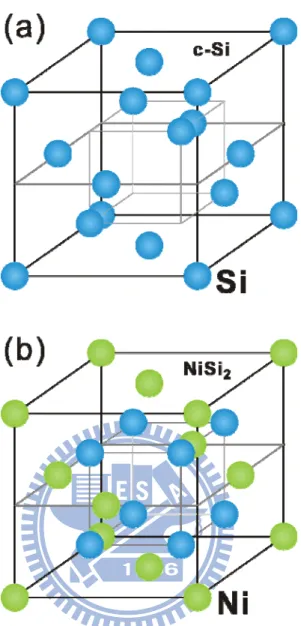
Figure 1‐2 shows the diamond structure of Si and the fluorite structure of NiSi2. The lattice constant of Si and NiSi2 is 5.430 Å and 5.406 Å, respectively, leading to very small lattice mismatch of 0.4 % with Si. The Ni‐metal is considerably suitable for the formation of epitaxial Si and is therefore employed for the fabrication of NILC poly‐Si films in this thesis. When a Ni film is deposited on a c‐Si substrate and annealed, the Ni2Si with PdCl2 structure forms at ~200oC and transforms into NiSi with the MnP structure at 350‐750oC. [43] These two phase‐transformations are diffusion‐controlled processes. Finally the NiSi transforms into the end phase NiSi2 by a nucleation‐controlled process at high transformation temperature in the range 450‐750oC. However, the NiSi transforming into the NiSi2 is a diffusion‐controlled process for the α‐Si. Hence it’s a low‐temperature process as 350oC for NiSi2 precipitate formation, as shown in Fig. 1‐3 [44]. Subsequently, the NiSi2 crystallites serve as the nuclei for crystallization. The diffusivity of Ni [45] in α‐Si is higher than that in c‐Si. Thus the needle‐like Si crystallite forms due to the diffusion of Ni in the α‐Si network.
Figure 1‐2 The crystalline structures: (a) the diamond structure of Si and (b) the fluorite structure NiSi2.
Figure 1‐3 The formation temperature map of thin‐film Ni silicides on (a) α‐Si, and (b) c‐Si [44].
Figure 1‐4 The equilibrium molar free‐energy diagram for NiSi2 in contact with α‐Si and c‐Si [38].
with α‐Si and c‐Si. Initially, several Ni‐Si phases form in the silicide region and the NiSi2 phase is found near the Si region [37]. The chemical potential of the Ni atoms is lower at the NiSi2/α‐Si interface and that of the Si atoms is lower at the NiSi2/c‐Si interface. Thus there is a driving force for Ni atoms diffusing through NiSi2 to α‐Si and for Si atoms diffusing reversely. This result indicates that the α‐Si is consumed at the NiSi2/α‐Si during the migration of NiSi2 crystallite. In 1993, C. Hayzelden and J. L. Batstone [38] found that a few layers of c‐Si exist at the leading edge of the NiSi2 precipitate. Therefore they propose a possible modification of the growth mechanism, as shown in Fig 1‐5. The nucleation of c‐Si on NiSi2 initially occurs and Si atoms then diffuse through NiSi2 to c‐Si, as illustrated in Fig 1‐5a. Next a c‐Si nucleates at the leading edge of a migrating NiSi2 precipitate. Ni atoms then diffuse through NiSi2 to α‐Si due to its ability to lower the chemical potential at the NiSi2/α‐Si, as shown in Fig 1‐5b. A fresh c‐Si forms at the NiSi2/α‐Si interface and the process repeats. Finally the needle‐like Si crystallite is formed after the migration of NiSi2 in a‐Si network, as shown in Fig 1‐5c
To enlarge poly‐Si grain size, SPC is typically carried out at 600oC to increase the incubation time and decrease the grain growth rate. Therefore a long annealing time is required for the SPC method. In the NIC/NILC method, a short annealing time and the low temperature (>600oC) could be obtained, because of lower energy barrier of crystallization resulting from the reaction between Ni‐metal and Si. However the undesirable Ni and NiSi2
Figure 1‐5 A possible modification of the c‐Si growth mechanism involving the formation of a thin layer of c‐Si at the α‐Si/NiSi2 interface [38].
precipitates would be trapped NILC poly‐Si grain boundaries. The metal gettering from Si is a candidate to solve this issue.
1.3 Metal Gettering from Silicon
Transition‐metals (Fe, Co, Ni and Pd) are ubiquitous in Si wafers, being introduced both during wafer growth and in subsequent processing. These metal impurities degrade the minority carrier lifetime and increase the leakage current. [46] The degradation of Si devices by metal impurities could be improved by metal gettering which is employed extensively in microelectronics and photovoltaics. In general, the gettering process involves three steps: (1) the release of the impurities from the device region, (2) the diffusion of the impurities to the gettered region, and (3) the capture of the impurities at the gettered region, as shown in Fig. 1‐6. [47] The energy barrier of the release of the impurities should be low and the captured impurities should not be release simply. Moreover, the distance between the captured region and the device region should be short; the impurities should diffuse quickly through the interface or the interlayer.
In 2000, S. M. Myers et al [48] proposed at least five distinct types of gettering mechanism, as follows: (1) metal‐silicide precipitation, (2) segregation into second phase, (3) atomic trapping by defects, (4) interaction with electronic dopants, and (5) phosphorous‐ diffusion gettering and nonequilibrium processes. Gettering by metal‐silicide precipitation
Figure 1‐6 The concept of the gettering process including release, diffusion, and capture of the metal impurities [47].
is an effective method to remove metal impurities from the device region. This mechanism, as introduced in chapter 1‐2‐2, has been implemented by back‐side polycrystalline silicon gettering [49]. The next mechanism also involves a second phase, but one formed by a third elemental species, with the transition metal being a dilute constituent. For example, gettering by segregation into a deposited Al can take place using Al–Si liquid on the back side of the wafer [50, 51]. That is because of a higher solubility of the metallic impurity in the liquid Al‐Si phase compared with that in solid Si.
The imperfections or defects in Si are expected to be the gettering sits. These defects are incompletely coordinated being associated with open regions in the lattice and with Si atoms and therefore reactive. S. M. Myers et al refers to such solute‐defect reactions not involving second‐phase formation as trapping, Most researchers introduce the cavities into Si to getter metal (Fe [52], Co [53], Ni [54, 55], Pt [56], Au [57, 58], and Cu [59, 60]) by ion‐implanting He or H. Trapping is believed to occur through a complex chemisorption‐like reaction on the cavity walls.
Most transition‐metal solutes are charged in Si and this characteristic can be developed for gettering by the electronic dopants. A charged metal atom and a dopant atom with opposite charge may form a bound pair, due to the electrostatic attraction. Moreover the energy of the charged metal atom is reduced, as the level of electronic doping is sufficient to
shift the Fermi level. Therefore metal impurity (Mn, Fe, and Co) segregates from an intrinsic or lightly doped region into a highly doped zone (B‐doped and P‐doped Si). [61, 62]
W. Schröter found that SiP precipitates form near Si/PSG interface in phosphorous‐ diffusion gettering and are capable of removing Ni impurities to produce NiSi2 particles [63]. An influence of SiP precipitation during gettering is suggested by metal‐silicide precipitation at the SiP particles. This phenomenon is also found during phosphorous‐ diffusion gettering of Pt [64].
These gettering methods have been effectively employed to reduce metallic impurities in Si. However these gettering methods are complicated and require high process temperatures. Even back‐side gettering by ion‐implanting damage is not suitable for TFTs device, due to a 500‐nm‐thick buffer oxide located between NILC poly‐Si and the Si substrate. Hence we proposed a gettering structure, as shown in Fig. 1‐7. [65‐67] The mechanism of gettering is classified in metal‐silicide precipitation. For effective gettering, the solubility of Ni impurities in the Ni gettering layer should be higher than that in the device region and the Ni diffusivity in the etching stop layer should be high. Thus the etching stop layer should be thin for Ni atoms diffusing quickly and well protect the device region during the removal of the Ni gettering layer. In addition, C.‐M. Hu proposed the contact holes gettering [68] and wafer bonding gettering [69] with no etching stop layers.
Figure 1‐7 (a) A gettering structure with a Ni gettering layer and an etching stop layer, and (b) the device region protected well by an etching stop layer during the removal of the Ni gettering layer.
1.4 Silicon Nanowires (NWs) Fabrication
Low temperature poly‐Si TFTs have been employed in flat panel displays. [1‐6] The major advantage of poly‐Si TFTs technology is its integration of driver electronics, sensors, memories, and peripheral circuits on the glass substrate for multifunctional active‐matrix displays. Several techniques have been proposed to scale down poly‐Si TFTs’ device geometries for increasing the device density. Unfortunately, the undesirable short‐channel effects (SCEs) in electrical characteristics have been found in the conventional planar short‐channel poly‐Si TFTs. Recently, lots of efforts on nonplanar device structures have been developed for better gate electrostatic control of the channel potential, such as nanowire channel. [70, 71] Si NWs with high surface‐to‐volume ratio feature have been adopted in memory devices [72], NW thin‐film transistors (TFTs) [73], and biosensors [74]. In general, Si NWs fabrication could be classified into two types: top‐down, and bottom‐up, introduced as follows:
1.4.1 Top-Down Method
Top‐down method generally requires the advanced lithography techniques, such as deep UV [75], e‐beam [76]. Fist, nano‐scale patterns are defined on the substrates and Si NWs then form by dry‐etching. These approaches are well developed for mass production, but very expensive equipments and cutting‐edge technologies are required. In addition,
several techniques, like thermal flow [77], chemical shrink [78], and spacer patterning [79] have been reported to assist the nano‐scale patterns fabrication by the conventional lithography tools (G‐line and I‐line steppers). The conventional lithography is relatively cheap for Si NWs fabrication.
1.4.2 Bottom-Up Method
In general, Si NWs fabricated by bottom‐up method need to be assembled and align for the electronics compared with top‐down method. The assembly techniques such as electric‐field‐directed assembly [80], microfluidic channel [81] and Langmuir‐Blodgett (LB) technique [82] have been proposed. Electric field method is via interaction between electric field of two parallel electrodes and polarity of NWs. Fluidic channel method could obtain assembled NW arrays by flowing NWs suspension inside a polydimethylsiloxane (PDMS) mold and LB method could assemble large‐area anisotropic NWs by a compression process.
Typically the bottom‐up method contains three steps: (a) deposition methods to prepare the NWs, (2) synthesis of the NWs on a substrate, and (3) dispersion of NWs into a solution. Some deposition methods have been proposed including, laser ablation catalyst growth [83], chemical deposition catalyst growth [84] and oxide‐assisted catalyst‐free method [85]. The first two techniques use a metal nanocluster catalyst as the nucleation
site for NWs growth. Hence metal contamination is a potential concern in this approach. Oxide‐assisted catalyst‐free method could fabricate NWs without metal contamination, but it is not adapted to electronic devices due to lots of defects in NWs.
Recently, H.‐C. Lin et al proposed a novel TFT structure with sidewall‐spacer poly‐Si nanowire channels. [86‐88] The feature of process is the simple method of forming sidewall‐spacer of MOSFET, as shown in Fig. 1‐8b. Here we fabricate NILC poly‐Si NWs TFTs similar to the sidewall‐spacer method to investigate the effect of Ni residues on the performance of NILC poly‐Si NWs TFTs.
1.5 Motivation and Thesis Organization
High‐performance low‐temperature polycrystalline silicon (poly‐Si) thin‐film transistors (TFTs) have attracted considerable interest for their application in flat panel displays. NILC is particularly attractive for forming superior, poly‐Si films with good electrical characteristics However, NILC poly‐Si grain boundaries trap Ni and NiSi2 precipitates which increase the leakage current and shift the threshold voltage.
Here, we propose a technique that could effectively resolve the Ni‐residue issues. Our method is using a gettering structure (Ni gettering layer/etching stop layer) to getter Ni impurities inside NILC poly‐Si based on metal‐silicide precipitation mechanism. It’s a simple and effective process for improving the electrical properties of large area NILC TFTs. To
Figure 1‐8 (a) Photoresist patterns on top of the poly‐Si surface by the conventional lithography, and (b) the sidewall spacer NW channels fabricated by an anisotropic etching.
reduce thermal budget of the previous PECVD‐SiNx gettering, around 5‐nm‐thick chemical oxide is proposed as an etching stop layer. This approach is compatible to traditional TFTs fabrication and costs cheaper compared with PECVD deposition. To further improve the gettering efficiency of α‐Si gettering layers, phosphorous dopant is introduced into α‐Si film. This is because phosphorous‐diffusion could obtain solubility enhancement of Ni impurities.
In addition to improving the performance of NILC poly‐Si thin‐film and NW channel transistors, the gettering of nickel impurities within NILC poly‐Si is carried out. Reduction of Ni‐related defects trapped in the channel layer due to NILC poly‐Si nature, could suppress the leakage current and negative shift of the threshold voltage. Moreover, NiSi2 precipitates are randomly trapped at poly‐Si/gate oxide interfaces and poly‐Si grain boundaries. Hence the uniformity of device performance could be improved through a Ni‐gettering process.
The dissertation is divided into five chapters listed below:
In chapter 1, an overview of poly‐Si TFTs is reviewed, and then the processes of low temperature poly‐Si crystallization, the metal gettering from Si, and Si NWs fabrication are introduced. Finally, the motivation of this study and the outline of the dissertation are provided.
In chapter 2, a simple and effective Ni‐gettering process is proposed to reduce Ni impurities inside NIC and NILC poly‐Si films. The phosphorous‐doped α‐Si/chemical oxide
served as a gettering structure is introduced. Moreover, the influence of the phosphorous dopant concentration on the gettering efficiency is investigated. In this chapter, we also compare the effects of the phosphorous dopant and the argon dopant on NILC rate.
In chapter 3, the effects of Ni‐gettering layers (p‐α‐Si/chem‐SiO2 films) on electrical characteristics of large area NILC TFTs is studied. The leakage current, threshold voltage, and the uniformity of NILC TFTs are studied after a Ni‐gettering process.
In chapter 4, the fabrication of NILC poly‐Si TFTs with a couple Si NWs is introduced. The effect of Ni residues on the performance of NILC poly‐Si NWs TFTs is investigated. The proposed gettering method is employed to improve the electrical characteristics of NILC poly‐Si NWs TFTs.
Chapter 2 Ni Reduction of Nickel-Mediated
Crystallization Polycrystalline Silicon
Using A Ni-Gettering Process
2.1 Introduction
Several metal gettering methods have been employed to reduce the amount of undesired metallic impurities in Si. However these gettering methods are complicated and require high process temperatures. In previous studies [65], we have proposed a simple method for reducing Ni concentration inside the NILC film. It involves using α‐Si and silicon‐nitride (SiNx) films as Ni‐gettering layers. The top α‐Si layer served as a gettering layer, while the middle SiNx layer was used as an etching stop layer. However the gettering time required was 90 h due to low Ni diffusivity in SiNx. To reduce the thermal budget of the Ni‐gettering process, we use α‐Si and chemical oxide (chem‐SiO2) films as Ni‐gettering layers, because Ni atoms transfer quickly through the nanothick‐SiO2 layer [89].
During the gettering process, Ni atoms were diffused from the NILC film to the α‐Si layer due to the concentration gradient. When the system reached equilibrium, no more Ni diffused into the gettering layer. At this point, the Ni concentration in the α‐Si layer was the
same as that in NILC. To improve the Ni‐gettering efficiency, phosphorus‐doped α‐Si (p‐α‐Si) films and chemical SiO2 (chem‐SiO2) layers are used as gettering layers. The effect of phosphorus dopant on the Ni‐gettering efficiency is investigated in this chapter.
2.2 Experimental Procedure
2.2.1 Gettering of Ni Residues from NILC Poly-Si Films
Three kinds of poly‐Si films are investigated in this study. One is a poly‐Si film fabricated by traditional NILC method without the gettering process (referred to as NoGET), and the others are poly‐Si films fabricated by the same NILC method with different Ni‐gettering layers (referred to as ASiGET and PSiGET). The NILC fabrication process began with capping 4‐inch Si (100) wafers with 500‐nm‐thick wet thermal oxide. Silane‐based 100‐nm‐thick α‐Si films were then deposited using low‐pressure chemical vapor deposition (LPCVD) at 550oC in N2 ambient. The photoresist was patterned to form desired Ni lines, and a 5‐nm‐thick Ni film was deposited on the α‐Si.
To form NoGET poly‐Si films, samples were annealed at 540oC for 24 h in N2 ambient, as shown in Fig. 2‐1a. The unreacted Ni was then removed by a mixed solution of H2SO4 and H2O2 for 20 min. Finally, poly‐Si films were dipped into 1% diluted hydrogen fluoride (DHF) solution to remove the annealing surface oxide, as illustrated in Fig. 2‐1b.
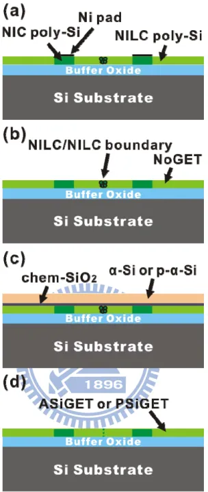
Figure 2‐1 Schematic illustration of the Ni‐gettering process: (a) fabrication of the NILC poly‐Si film, (b) removal of unreacted Ni pads, (c) capped with an etching stop layer (chem‐SiO2) and a gettering layer (α‐Si or p‐α‐Si), and (d) removal of the gettering layer and the chem‐SiO2 layer.
H2SO4 and H2O2 for 10 min to form a chem‐SiO2 layer on the top of NILC poly‐Si films. A 100‐nm‐thick α‐Si film was then deposited on the chem‐SiO2 layer using LPCVD at 550oC for 1 h in N2 ambient, as shown in Fig. 2‐1c. The top α‐Si film served as the Ni‐gettering layer.
As for the PSiGET poly‐Si films, phosphorus ions were implanted into α‐Si to form a p‐α‐Si film, as shown in Fig. 2‐1c. The projection range (Rp) of ions was set at the middle of the α‐Si film. The ion‐accelerating energy was 35 keV. The dosage of phosphorus ions were 1×1014 cm‐2, 1×1015 cm‐2 and 1×1016 cm‐2, respectively. Relevant parameters for the samples studied are summarized in Table 2‐1.
Samples undergoing Ni‐gettering were then annealed at 550oC for 12 h in N2 ambient with the goal of removing the unwanted Ni metal inside the NILC poly‐Si. Following the annealing process, the top Ni‐gettering films were removed using 5% tetramethylammonium hydroxide (TMAH) solution for 2 min at 55oC, and the chem‐SiO2 layers were removed using 1% DHF solution, as illustrated in Fig. 2‐1d. For the purpose of comparison, the NoGET poly‐Si film was also subjected to an extended heat treatment at 550oC for 12 h in N2 ambient.
2.2.2 Gettering of Ni Residues from NIC Poly-Si Films
The fabrication process of NIC poly‐Si is shown in Fig. 2‐2. Silane‐based 100‐nm‐thick α‐Si films were deposited using LPCVD at 550oC in N2 ambient, as displayed in Fig. 2‐2a. A
Table 2‐1 Relevant parameters of the Ni‐gettering layers.
Figure 2‐2 Schematic illustration of the Ni‐gettering process of the NIC poly‐Si: (a) fabrication of the NIC poly‐Si film (b) removal of unreacted Ni films, and (c) capped with a chem‐SiO2 layer and a gettering layer (α‐Si or p‐α‐Si).
5‐nm‐thick Ni film was then deposited on the α‐Si, and subsequently annealed at 540oC for
24 h to form NIC poly‐Si. The unreacted Ni was then removed by a mixed solution of H2SO4 and H2O2 for 20 min. Finally, poly‐Si films were dipped into 1% DHF solution to remove the annealing surface oxide, as shown in Fig. 2‐2b. The poly‐Si film was dipped into a mixed solution of H2SO4 and H2O2 to form a chem‐SiO2 layer. A 100‐nm‐thick α‐Si film was then deposited on the chem‐SiO2 layer using LPCVD at 550oC for 1 h in N2 ambient to form the α‐Si gettering layer, as illustrated in Fig. 2‐2c. Phosphorous ions were implanted into α‐Si to form the p‐α‐Si gettering layer. The dosage of phosphorus ions and the ion‐accelerating energy were 1×1016 cm‐2 and 35 keV, respectively. Samples were then annealed at 550oC for 12 h in N2 ambient.
2.2.3 Dopant Effect on NILC Rate
Three kinds of α‐Si films are investigated in this study. One is intrinsic α‐Si, and the others are α‐Si films introduced by argon ions and phosphorus ions, respectively. First, silane‐based 100‐nm‐thick α‐Si films were deposited on oxide Si substrates using LPCVD, followed by ion implantation. The Rp of ions was then set at the middle of the α‐Si film and the dosage was 1×1014 cm‐2, 1×1015 cm‐2, and 1×1016 cm‐2, respectively. Then 5‐nm‐thick Ni lines were selectively deposited on sample surfaces. Finally the traditional NILC method was carried out at 540oC for 16 h in N2 ambient.
2.3 Results and Discussion
2.3.1 Characterization of NILC Poly-Si Films
The length of the NILC poly‐Si is about 79μm and almost saturated, as shown in Fig. 2‐3. Since solid‐phase crystallization (SPC) poly‐Si grains formed near interface between α‐Si and NILC poly‐Si, the NILC poly‐Si grains laterally growth was blocked. Therefore we can obviously see the winding interface (α‐Si/NILC poly‐Si). Before the NILC got saturated, we can examine NICL rate as 3.59 μm/h, as shown in Fig. 2‐4.
After a NILC fabrication process, the α‐Si and Ni silicide were etched away with Secco etching solution [90] and examined by scanning electron microscope (SEM). The NILC poly‐Si is composed of needle‐like poly‐Si grains and grain size is about 100 nm, as displayed in Fig. 2‐5.
2.3.2 Quality of chem-SiO2 Layers
To examine the quality of the chem‐SiO2 film, after the chem‐SiO2 layer was formed, platinum was deposited on top of the chem‐SiO2 film for image contrast in transmission electron microscopy (TEM) sample preparation. As shown in Fig. 2‐6, the oxide layer is only about 5 nm thick. This chem‐SiO2 layer was used as an etching stop layer in the 5% TMAH etching solution. Moreover, this nano oxide layer also served as a diffusion interlayer during the Ni‐gettering process. Ni atoms needed to diffuse from the NILC poly‐Si through
Figure 2‐3 OM image of the α‐Si film after a NILC process carried out at 540oC for 24 h in N2 ambient.
Figure 2‐4 The dependence of the NILC length on the anneal time. The NILC was carried
Figure 2‐5 SEM image of the NILC poly‐Si grains treated with Secco‐etching.
Figure 2‐6 (a) Cross‐sectional TEM images of the NILC Poly‐Si films capped with the chemical oxide films, and (b) the high magnification of a chemical oxide film around 5 nm thick. Platinum (Pt) films were deposited on top of the chem‐SiO2 layers for image contrast.
the thin chem‐SO2 into the Ni‐gettering layer. The chem‐SiO2 in Fig. 2‐6b tends to be porous and amorphous. Therefore Ni atoms possibly diffused through 5‐nm‐thick chem‐SiO2 faster compared with 30‐nm‐thick SiNx [65] used before.
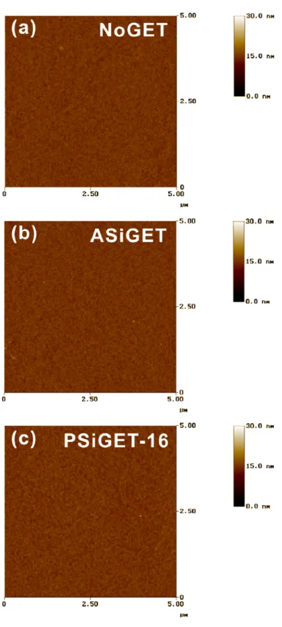
To study the effect of Ni‐gettering on the surface roughness of the NILC poly‐Si after gettering layers removal, the NILC poly‐Si surfaces were measured using atomic force microscopy (AFM). As shown in Fig 2‐7, the metal gettering did not change the surface roughness greatly: the root‐mean‐square (RMS) roughness of ASiGET (0.65 nm) and PSiGET‐16 (0.69 nm) are almost the same as that of NoGET (0.64 nm). This seems that 5‐nm‐thick chem‐SiO2 layer did protect ASiGET and PSiGET‐16 poly‐Si surfaces during wet etching by 5% TMAH solution.
2.3.3 Ni-Gettering Using chem-SiO2 Interlayer
Figure 2‐8a shows the optical microscopy (OM) images of the Ni‐gettering layers after it was deposited on top of the chem‐SiO2 layer using LPCVD at 550°C for 1 h in N2 ambient. The pink region is α‐Si and the green regions are disk‐like poly‐Si. This result indicates that during the deposition of α‐Si film, some Ni atoms had already diffused from the NIC area through the chem‐SiO2 layer into the gettering layer and caused α‐Si to be transformed into poly‐Si grains by the NILC mechanism. However in the case of the α‐Si/SiNx‐gettering process [65], no NILC poly‐Si was observed on the gettering layer during the deposition of
Figure 2‐7 AFM images of the NILC poly‐Si surfaces (a) without Ni‐gettering, and with Ni‐gettering by (b) a α‐Si layer, and (c) a p‐α‐Si layer (the dosage was 1×1016 cm‐2).
Figure 2‐8 OM images of the Ni‐gettering layers: (a) a α‐Si film deposited on a chem‐SiO2
layer by LPCVD and then phosphorous ions implanted at a dosage of (b) 1×1014 cm‐2, (c) 1×1015 cm‐2, and (d) 1×1016 cm‐2, respectively.

![Figure 1‐3 The formation temperature map of thin‐film Ni silicides on (a) α‐Si, and (b) c‐Si [44].](https://thumb-ap.123doks.com/thumbv2/9libinfo/8710445.199945/26.892.310.629.107.802/figure-formation-temperature-map-film-ni-silicides-si.webp)