行政院國家科學委員會專題研究計畫 成果報告
過渡性金屬氧化物及硫屬化合物單晶與奈米結構之製備,
特性研究及其可能應用之探討(3/3) 研究成果報告(完整版)
計 畫 類 別 : 個別型
計 畫 編 號 : NSC 96-2112-M-011-001-
執 行 期 間 : 96 年 08 月 01 日至 97 年 10 月 31 日 執 行 單 位 : 國立臺灣科技大學電子工程系
計 畫 主 持 人 : 黃鶯聲
計畫參與人員: 碩士班研究生-兼任助理人員:王必先 碩士班研究生-兼任助理人員:黃進緯 碩士班研究生-兼任助理人員:李孟勳 碩士班研究生-兼任助理人員:戴棋緯 碩士班研究生-兼任助理人員:陳奎羽 碩士班研究生-兼任助理人員:施勇志 碩士班研究生-兼任助理人員:黃文彥 碩士班研究生-兼任助理人員:黃彥能 碩士班研究生-兼任助理人員:紀建光 碩士班研究生-兼任助理人員:葉建男 博士班研究生-兼任助理人員:許宏彬 博士班研究生-兼任助理人員:陳麒安 博士班研究生-兼任助理人員:陳宜民
報 告 附 件 : 出席國際會議研究心得報告及發表論文
處 理 方 式 : 本計畫可公開查詢
中 華 民 國 97 年 11 月 13 日
I
行政院國家科學委員會補助專題研究計畫 ■ 成 果 報 告
□ 期中進度報告 過渡性金屬氧化物及硫屬化合物之製備、特性研究
及其可能應用之探討
Growth, Characterization and Applications of Transition Metal Dioxide and Dichalcogenide Compounds
計 畫 類 別 : ■ 個 別 型 計 畫 □ 整 合 型 計 畫 計畫編號:NSC94-2112-M-011-001,NSC95-2112-M-011-001, NSC96-2112-
M-011-001
執行期間: 94 年 8 月 1 日 至 97 年 10 月 31 日
計 畫 主 持 人 : 黃 鶯 聲
計畫參與人員: 許宏彬、陳麒安、陳宜民
國立台灣科技大學電子工程所博士班研究生
王必先、黃進緯、李孟勳、戴棋緯、陳奎羽、施勇志、
黃文彥、黃彥能、紀建光、葉建男
國立台灣科技大學電子工程所碩士班研究生
成果報告類型(依經費核定清單規定繳交):□精簡報告 ■完整報告
執行單位:國立台灣科技大學電子工程所
中 華 民 國 97 年 11 月 13 日
II
一、中文摘要
本計畫主要反應式濺鍍法與有機金屬化學汽相沈積法成長過渡性(異質)金屬氧化物、二 氧化釕(IrO2)、二氧化銥(RuO2) 、二氧化鈦(TiO2)奈米結構晶體,並利用X光繞射(XRD)、
場發射式掃瞄式電子顯微鏡(FESEM)、拉曼散射實驗(Raman scattering)、與X光光電子發 射譜(XPS)來檢測所成長之奈米晶體物理與光學之特性,除此之外也利用場發射穿透式電子顯 微鏡(TEM)來觀測奈米晶體細微結構成長機制。另外也利用場發射實驗來觀測其不同形貌方向 之IrO2、RuO2 、TiO2一維奈米晶體。另一方面,也利用化學汽相傳導(chemical vapor transport method)方法成長不同摻雜之MoS2, MoSe2, WS2, WSe2, ReS2, ReSe2層狀單晶,另外也利用極化 的光導(photoconductivity), 表面光電壓 (surface photovoltage spectroscopy),調製光譜(modulation spectroscopy)及吸收(absorption)來量測層狀單晶的特性,此外也利用溫度變化(12 K-300 K)的實 驗來量測此樣品之特性,利用Varshni及Bose-Einstein方程式來得到其溫度變化之相關係數並加 以討論。
關鍵詞:過 渡 金 屬 硫 屬 化 合 物 、過 渡 金 屬 氧 化 物 、層狀單晶、奈米晶體、化學汽相傳輸 法、有機金屬化學汽相沈積法、調制反射式光譜、X 光繞射、X 光光電子發射譜、拉曼散 射、掃瞄式電子顯微鏡、穿透式電子顯微鏡
III
Abstract
We report the results of synthesis of well-aligned TiO2, IrO2 and RuO2 nanocrystals (NCs) via reactive magnetron sputtering and metal-organic chemical vapor deposition. The surface morphology and structural properties of the as–deposited NCs were characterized. A strong substrate effect on the alignment of the TiO2, IrO2 and RuO2 NCs deposition has been revealed in terns of field emission scanning electron microscopy (FESEM) micrographs The roles of different substrates in the formation of various textures of nanocrystalline TiO2, IrO2 and RuO2 are studied and the possible mechanisms have been discussed.
Raman spectroscopy (RS) has been used as a technique for the characterization of well-aligned TiO2,
IrO2 and RuO2 nanocrystals (NCs) grown on a number of different oriented substrates under various conditions. The relative intensity of the three strongest Raman-active modes, namely, the A1g, B2g and Eg modes, depends on the orientation of NCs and has been used to determine the preferred growth direction of the NCs. The redshifts and asymmetric linewidth broadening of the Raman features of IrO2 and RuO2 NCs with respect to that of their bulk counterparts were analyzed by a modified spatial correlation (MSC) model, which includes a factor of stress-induced shift. The MSC model showed that the effects of stress and nanometric size could be separated in analyzing the observed Raman features.
The usefulness of experimental RS together with the MSC model analysis as a structural and residual stress characterization technique for NCs has been demonstrated.
Chemical vapor transport (CVT) process with Br2 as a transporting agent has been utilized for growing large size MoS2, MoSe2, WS2, WSe2, ReS2, ReSe2 single crystals. The anisotropy of the direct and indirect band gap parallel and perpendicular to the crystal c (or b)-axis are characterized by polarization dependent piezoreflectace, photoreflectance, surface photovoltage spectroscopy and photoconductivity. The parameters that describe the temperature dependence of the indirect absorption edges and direct excitonic transitions are evaluated by the Varshni and Bose–Einstein empirical expression.
Keywords : Transition Metal Dichaclogenide, Transition Metal Oxide, Layer Crystals, Nanocrystals, Chemical Vapor Transport, Metalorganic Chemical Vapor Deposition, Modulation Spectroscpoy, X- Ray Diffraction, Raman Scattering, X-Ray Photoelectron Spectroscopy, Scanning Electron Microscpopy, Transmission electron microscopy, 1-D RuO2 NCs, 1-D IrO2 NCs, 1-D TiO2
NCs, Heteronanocrystals.
IV
二、計畫緣由與目的
近幾年來,過渡金屬硫屬化合物在光電化學及能源工業應用方面,頗受重視。其中 MoS2
的用途甚廣,因其本身質軟,潤滑性佳,對高溫高壓的穩定性好,是其他潤滑劑所無法比擬 的。而用於碳氫化合物中,則是加氫、去氫的良好催化劑。近年來更被用為作石油中加氫去
硫的主要觸媒。而在照光後產生 d-d 能帶間的轉換,不須破壞化學鍵,即不產生光腐蝕的現
象,可作為光電化學太陽電池的理想電極。過渡金屬硫屬化合物(Dichalcogenides), 層狀 結構者:如、二硒化鉬(MoS2), 二硒化鉬鈮(MoSe2), 二硫化鎢(WS2), 二硫化鎢鈮(WSe2), 二硫化錸(ReS2), 二硫化錸鈮(ReSe2)、等皆具有半導體之特性。過渡金屬氧化物( Dioxides )。
近幾年來,在光電化學及能源工業應用方面,頗受重視。其中二硫化鉬的用途甚廣,因其本 身質軟,潤滑性佳,對高溫高壓的穩定性好,是其他潤滑劑所無法比擬的。而用於碳氫化合 物 中 , 則 是 加 氫 、 去 氫 的 良 好 催 化 劑 。 近 年 來 更 被 用 為 作 石 油 中 加 氫 去 硫
(Hydrodesulfurization)的主要觸媒。而在照光後產生 d-d 能帶間的轉換,不須破壞化學鍵,
即不產生光腐蝕(Photocorrosion)的現象,可作為光電化學太陽電池的理想電極。因此若能 有效的探討其基本物性,對於實際應用上極有價值。在應用鐵電材料做為記憶體的介電層 時,不同於以往所使用的介電材料,在製程技術上仍有所多未克服的難題,在底電極的下方 為阻擋層,上方為鐵電性材料,故底電極材料的特性將直接影響鐵電薄膜的特性,進而影響 元件特性的優劣。而底電極材料的主要考量要素,有漏電流的大小、電阻值、高溫時是否易 氧化、可靠性、附著性及蝕刻性。Pt(鉑)是目前最常用的電極材料,但因其不易蝕刻與低 附著性,顯示 Pt 在未來製程中的不便性。而 Ir、IrO2/Ir、Ru、RuO2/Ru 則是近來廣為受到注 目的新興電極材料。TiO2,RuO2,IrO2雖為氧化物,但具有金屬般的導電性,是近來廣受注
目的新興電極材料,在光電化學及能源工業應用方面,也頗受重視。應用上尚有以 RuO2 與
CdS 組成蕭特基界面應用於積體光學,與玻璃混合燒結製成厚膜電阻,利用 RuO2 薄膜作為
VLSI 中阻擋鋁擴散之屏障,利用 RuO2 薄膜與 SrTiO3 製作高效率的 DRAM。IrO2與 RuO2奈
米結構可作為元件中理想的場發射材料。因此若能有效的探討 IrO2與RuO2的基本物性,對於
實際應用於元件上極有價值。至於 TiO2因期結晶特性有銳鈦礦(Anatase)、金紅石(Rutile)等晶 相,將其銳鈦礦二氧化鈦因為本身有極佳的光化學特性因此被利用於光觸煤應用,至於金紅 石二氧化鈦因為自身擁有高介電常數之光學特性所以常用於光學鏡片之鍍膜等應用,除此之 外也常應用於綠色能源-太陽能電池(Solar cell)之電極與表層導電玻璃(ITO)之介面層。
三、研究方法及計畫成果 研究方法
1. 利用反應式濺鍍法法成長 RuO2, IrO2一維奈米晶體。
2. 利用有機金屬化學汽相沈積法成長 TiO2, RuO2, IrO2一維奈米晶體。
3. 利用 X 光繞射與拉曼散射實驗檢測 TiO2,RuO2, IrO2 一維奈米晶體之結構特性及結晶相 變化。
4. 利用掃瞄式電子顯微鏡檢視 TiO2,RuO2, IrO2一維奈米晶體之表面結晶狀況。
5. 利用拉曼光譜檢視 TiO2, RuO2, IrO2 一維奈米結構因為應力與尺寸效應所個別造成拉曼 光譜訊號紅移的現象。
6. 利用 X 光光電子發射譜檢測 TiO2, RuO2, IrO2一維奈米晶體之成分與固態鍵結狀態。
7. 利用穿透式電子顯微鏡檢視TiO2, RuO2 與IrO2 一維奈米晶體與異質奈米晶體之細微結構。
8. 利用光導(photoconductivity)來量測MoS2, MoSe2, WS2, WSe2, ReS2, ReSe2層狀單晶的特性。
9. 利用電阻率(resistively)及霍爾效應(Hall effect)量測技術來量測MoS2, MoSe2, WS2, WSe2,
V
ReS2, ReSe2層狀單晶的特性。
10. 利用調製光譜(modulation spectroscopy)來量測MoS2, MoSe2, WS2, WSe2, ReS2, ReSe2層狀單晶 的特性。
11. 利用表面光電壓(surface photovoltage)來量測MoS2, MoSe2, WS2, WSe2, ReS2, ReSe2層狀單晶 的特性。
12.溫度變化(12K-300K)的光導(photoconductivity)實驗來量測MoS2, MoSe2, WS2, WSe2, ReS2, ReSe2層狀單晶。
13.溫度變化(12K-300K)的電阻率(resistively)及霍爾效應(Hall effect)實驗來量測MoS2, MoSe2, WS2, WSe2, ReS2, ReSe2層狀單晶。
研究計畫相關成果:
計畫執行期間發表層狀半導體及奈米氧化物相關論文共 44 篇
I. Layered Crystal Semiconductors
1. Dumcenco, D. O., Y. S. Huang, C. H. Liang, and K. K. Tiong, “Optical characterization of Au- doped rhenium diselenide single crystals,” J. Appl. Phys., Vol. 104, 063501 (2008).
In this paper, the optical properties of Au-doped rhenium diselenide (ReSe2:Au) single crystals have been reported. The doping effects of the material were characterized by polarization dependent transmittance, piezoreflectance (PzR) and photoreflectance (PR) measurements in the temperature range of 15–300 K. The indirect energy gap of ReSe2:Au shows a slight red-shift with respect to the undoped sample. The low temperature PzR and PR spectra reveal an E1ex feature at E||b polarization as well as two features,
E2ex and E3ex, at E⊥b polarization. The angular dependence of the excitonic feature amplitudes agrees well with Malus’ law. In comparison with the undoped ReSe2, the excitonic transition energies remain practically unchanged, while the broadening parameter of the excitonic transition features slightly increases due to impurity scattering. In addition, the parameters that describe the temperature variations of the band-edge excitonic transitions were evaluated and discussed.
2. Liang, C. H., C. H. Chen, K. K. Tiong, D. O. Dumcenco and Y. S. Huang, “In-plane anisotropic electrical and optical properties of gold–doped rhenium disulphide,” Journal of Materials Science:
Materials in Electronics, DOI 10.1007/s10854-008-9685-2.
Au-doped ReS2 layer crystals were grown by chemical vapour method with iodine as the transport agent. Room temperature Hall effect measurement showed p-type semiconducting character for the doped sample. The electrical conductivities parallel and perpendicular to the crystal b-axis were investigated. The near band-edge temperature- dependent in-plane anisotropic optical properties were studied by the polarization-dependent photoconductivity measurements, with the incident light beam parallel and perpendicular to the crystal b-axis, in the temperature range from 20 to 300 K. The influence of Au in the measured conductivity anisotropy and photoconductivity spectra of doped ReS2 were analysed and discussed.
3. Ho, C. H., S. T. Wang, Y. S. Huang, and K. K. Tiong, “Structural and luminescent property of gallium chalcogenides GaSe1-xSx layer compounds,” Journal of Materials Science: Materials in Electronics, DOI 10.107/s10854-007-9539-3.
Structural and luminescence properties of GaSe1-xSx (0 ≤ x ≤1) series optical materials have been studied by X-ray diffraction, photoluminescence (PL), and piezoreflectance (PzR) measurements. Powder X-ray diffraction patterns showed the whole series layers present three different kinds of stacking formula with respect to the compositional change of sulfur from x = 0 to 1. The PL results show the whole series GaSe1-xSx layers emit the luminescences from red to blue visible region. The PL and PzR spectra of the GaSe1-xSx are analyzed. The structural variation in between the layers is discussed.
4. Dumcenco, D. O., H. P. Hsu, Y. S. Huang, C. H. Liang, K. K. Tiong, and C. H. Du, “Optical properties of tungsten disulfide single crystals doped with gold,” Mater. Chem. Phys., Vol. 111, pp.
VI
475~479 (2008).
Single crystals of WS2 doped with gold have been grown by the chemical vapor transport method using iodine as a transporting agent. X-ray diffraction (XRD) pattern analysis revealed presence of mixed three-layer rhombohedral (3R) and two-layer (2H) hexagonal polytypes for the doped crystals while the undoped one shows only 2H form. Hall measurements indicate that the samples are p-type in nature. The doping effects of the materials are characterized by surface photovoltage (SPV), photoconductivity (PC) and piezoreflectance (PzR) measurements. Room temperature SPV and PC spectra reveal a feature located at ~60 meV below the A exciton and has been tentatively assigned to be an impurity level caused by Au dopant. The excitonic transition energies of the A, B, d and C excitons detected in PzR spectra show red shift due to the presence of a small amount of Au and the broadening parameters of the excitonic transition features increase due to impurity scattering. The values of the parameters that describe the electron (exciton)-phonon interaction of excitonic transitions of A–B are about two times larger than that of d–C excitonic pairs. The possible assignments of the different origins of A–B and d–C excitonic pairs have been discussed.
5. Lee, Y. C., S. Y. Hu, K. K. Tiong, J. L. Shen, K. W. Chen, and Y. S. Huang, “Temperature dependence anisotropic photoconductivity in 2H-MoSe2 single crystals,” J. Alloy. Compd., Vol.
448, pp. 44~48 (2008).
Single crystals of 2H-MoSe2 were investigated by the anisotropic photoconductivity (PC) measurements as a function of temperature in the range of 12–300 K. A significant shift towards lower energy has been observed in the PC spectra of the edge plane with respect to the van der Waals plane. The anisotropy in the indirect energy gap is being attributed to crystal anisotropy.
The parameters that describe the temperature dependence of the anisotropic indirect energy gap are evaluated and discussed utilizing the Varshni and Manoogian–Woolley semi-empirical relationships. The Debye temperature of the sample has also been estimated by the fitted values.
6. Dumcenco, D. O., Y. S. Huang, C. H. Liang, and K. K. Tiong, “Optical characterization of niobium-doped rhenium disulphide single crystals,” J. Appl. Phys., Vol. 102, 083523 (2007).
In this study, the optical properties of niobium-doped rhenium disulphide (ReS2: Nb) single crystals have been reported. The doping effects of the material were characterized by polarization-dependent transmittance, photoluminescence PL, and piezoreflectance PzR measurements in the temperature range of 10–300 K. The indirect energy gap of ReS2: Nb shows a slight redshift with respect to the undoped sample. The low temperature PL spectra reveal two near direct band-edge excitonic peaks as well as two additional prominent features at higher energy side. The results agree well with that of the PzR investigation of the sample. In comparison with the undoped ReS2, the excitonic transition energies remain practically unchanged, while the broadening parameter of the excitonic transition features slightly increases due to impurity scattering. In addition, the parameters that describe the temperature variations of the band-edge excitonic transitions were evaluated and discussed.
7. Ho, C. H., M .H. Hsieh, C. C. Wu, Y. S. Huang, and K. K. Tiong, “Dichroic optical and electrical properties of rhenium dichalcogenides layer compounds,” J. Alloy. Compd., Vol. 442, pp. 245~248 (2007).
Dichroic optical and electrical behaviors of layered ReX2 (X = S, Se) have been characterized using angular dependent polarized- absorption and resistivity measurements in the van der Waals plane. The polarized energy gaps of ReS2 and ReSe2 were analyzed from the polarized-absorption spectra with polarization angles from θ = 0º (E || b-axis) to θ = 90º (E⊥b-axis). The angular- dependent relationships of the polarized energy gaps of ReX2 were analyzed. Angular dependent resistivity measurements of ReX2
were carried out in the layer plane. The cutting edge of each sample was varied from θ = 0º (|| b) to θ = 120º with an increment of 10º with respect to the layer crystal’s b-axis. The angular dependency of the resistivities in the layered plane was analyzed. The experimental evidences of angular dependent in-plane resistivities and polarized energy gaps of ReX2 (X = S, Se) show that for ReX2 not only an optical dichroism but also an electrical dichroism in the van der Waals plane occurs.
8. Hu, S. Y., C. H. Liang, K. K. Tiong, Y. S. Huang, “Effect of Re and Nb dopants on the electrical and optical properties of MoSe2 single crystals,” J. Alloy. Compd., Vol. 442, pp. 249~251 (2007).
Chemical vapor transport (CVT) process with Br2 as a transporting agent has been utilized for growing large size MoSe2 single crystals by adding Re (rhenium) dopant (nominal concentration of ∼1%) during the growth process. The maximum size crystals are about 10 mm ×10 mm in surface area and 2 mm in thickness. The large edge plane facilitates easier study of the influence of crystal anisotropy on the electrical and optical properties of the layered crystals. The anisotropy of the conductivity and indirect band gap parallel and perpendicular to the crystal c-axis due to the interlayer van der Waals interaction and red shift of the indirect and direct band gaps due to doping have been measured. It is found that the conductivity anisotropy decreases drastically as a result of doping and the crystal anisotropy has a more pronounced influence on the indirect gap in comparing to the direct gap of the layered crystals.
9. Hu, S. Y., Y. C. Lee, J. L. Shen, K. W. Chen, and Y. S. Huang, “Urbach tail in the absorption spectra of 2H-WSe2 layered crystals,” phys. stat. sol. (a), Vol. 204, pp. 2389~2395 (2007).
VII
Urbach’s rule and steepness parameter of 2H-WSe2 layered crystals have been studied via the absorption spectra from the photoconductivity (PC) measurements in the temperature range of 15–300 K. From the analysis of the temperature-dependent band gap with Varshni semi-empirical equation, the Debye temperature was estimated as 160 K while the Einstein temperature was around 125 K from the Einstein oscillator model. The effective phonon energy was estimated successfully from the temperature dependence of the Urbach energy extracted from the PC spectra and the value was found out to be well correlated to the active E1g
mode observed in the Raman spectra of 2H-WSe2.
10. Hu, S. Y., Y. Z. Chen, K. K. Tiong, and Y. S. Huang, “Growth and characterization of molybdenum-doped rhenium diselenide,” Mater. Chem. Phys., Vol. 104, pp. 105~108 (2007).
Single crystals of molybdenum-doped ReSe2 have been grown by chemical vapor transport (CVT) process with Br2 as a transporting agent. XRD has been used to confirm the triclinic-layered structure of the as-grown undoped and doped samples. The optical properties are studied by anisotropic photovoltage and electrolyte electroreflectance measurements at 300 K. Both indirect and direct transition energies of the doped samples all show different degrees of red shifts for molybdenum-doped samples. The broadening parameters of the excitonic transition features broadened significantly for Mo-doped ReSe2 due to impurity scattering in layered structures. The electrical properties are investigated by the anisotropic conductivity and Hall measurements at 300 K. The influence of optical and electrical properties from the molybdenum dopant were compared and discussed.
11. Hu, S. Y., C. H. Liang, K. K. Tiong, Y. S. Huang, and Y. C. Lee, “Electrical anistropy of W-doped ReSe2 crystals,” J. Electrochem. Soc., Vol. 153, pp. J100~J102 (2006).
Single crystals of W-doped ReSe2 have been grown by chemical vapor transport process with bromine as the transporting agent.
Single crystalline platelets up to 3 x 3 mm2 surface area and 100 μm in thickness were obtained. From the X-ray diffraction patterns, the doped crystals are found to crystallize in the triclinic-layered structure. The electrical anisotropy has been investigated along and perpendicular to the b-axis on the van der Waals plane by temperature-dependent conductivity and Hall effect measurements. The influence of the dopant will be compared and discussed.
12. Hu, S. Y., Y. C. Lee, J. L. Shen, K. W. Chen, K. K. Tiong, and Y. S. Huang, “Temperature dependence of absorption edge anisotropy in 2H-MoSe2 layered semiconductors,” Solid State Communications, Vol. 139, pp. 176-180 (2006).
The absorption-edge anisotropy of 2H-MoSe2 was studied by photoconductivity (PC) measurements as a function of temperature in the range of 12–300 K. A significant shift towards lower energies has been observed in the PC spectra on the edge plane with respect to those corresponding to the van der Waals (VdW) plane. The parameters that describe the temperature dependence of the absorption edges are evaluated by the Bose–Einstein empirical expression. Effective phonon energy was estimated from the temperature dependence of the Urbach energy. The estimated effective phonon energy for the VdW and edge planes, respectively, can be correlated to the observed Raman active E1g and A1g modes.
13. Lee, Y. C., J. L. Shen, K. W. Chen, W. Z. Lee, S. Y. Hu, K. K. Tiong, and Y. S. Huang,
“Observation of persistent photoconductivity in 2H-MoSe2 layered semiconductors,” J. Appl.
Phys., Vol. 99, 063706 (2006).
We report the observation of persistent photoconductivity (PPC) effect in 2H-MoSe2 layered semiconductors. The decay behavior of PPC can be well described by a stretch-exponential function. Experimental results indicate that the lattice relaxation of DX-like impurity is responsible for PPC in MoSe2. In addition, the small capture barrier created by lattice relaxation and the temperature- dependent resistance measurement exhibit that the magnitude of PPC effect in MoSe2 is small, consistent with the PPC behavior in indirect gap materials.
14. Hu, S. Y., C. H. Liang, K. K. Tiong, Y. C. Lee, and Y. S. Huang, “Preparation and characterization of large niobium-doped MoSe2 single crystals,” J. Cryst. Growth, Vol. 285, pp. 408~414 (2005).
Chemical vapor transport (CVT) process with bromine as a transporting agent has been utilized for growing largesize MoSe2 single crystals by adding niobium dopant (nominal concentration = 0.5%) duringthe growth process. The maximum-size crystals are about 10 x 10mm2 in surface area and 2 mm in thickness. The large edge plane facilitates an easier study of the influence of crystal anisotropy on the electrical and optical properties of the layered crystals. Anisotropy of the conductivity and indirect band gap parallel and perpendicular to the crystal c-axis due to the interlayer van der Waals interaction and red shift of the indirect and direct band gaps due to doping have been measured. It is found that the electrical and optical properties of niobium-doped MoSe2 are almost similar to those of the pure MoSe2 single crystal apart from a drastic reduction in the conductivity anisotropy and red shift of the band gap.
15. Hu, S. Y., M. C. Cheng, K. K. Tiong, and Y. S. Huang, “The electrical and optical anisotropy of rhenium-doped WSe2 single crystals,” J. Physics: Conden. Matter, Vol. 17, pp. 3575~3583 (2005).
VIII
Single crystals of rhenium-doped WSe2 with large edge plane have been grown by the chemical vapour transport method using bromine as the transporting agent. From the x-ray diffraction patterns, both the doped and undoped crystals are found to crystallize in the 2H structure. The role of rhenium in affecting both the electrical and optical properties of the WSe2 crystals is examined. The thicker Re-doped WSe2 samples enable easier exploration of the electrical and optical anisotropies of the materials both parallel and perpendicular to the crystal c-axis. The samples are n-type in nature from Hall measurements and the conductivity anisotropy decreases drastically as a result of doping. Photovoltage measurements revealed that both undoped and Re-doped WSe2 are indirect semiconductors. The indirect band gap of the doped sample showed considerable red shift compared with the undoped sample and also exhibited anisotropy along and perpendicular to the c-axis. The anisotropy in the band gap is attributed to crystal anisotropy, which was also studied via the polarizationdependent electrolyte electroreflectance measurements taken along the van der Waals plane (E⊥c; k || c) and the as-grown edge plane (E⊥c, E || c; k⊥c). The strong dependence of excitonic transitions A and B on polarization compared with that of the undoped samples.
16. Wu, C. C., C. H. Ho, J. Y. Wu, S. L. Lin, and Y. S. Huang, “Characterization of Ge(Se1-xSx)2 series layered crystals grown by vertical Bridgman method,” J. Cryst. Growth, Vol. 281, pp. 377~383 (2005).
Single crystals of Ge(Se1−xSx)2 with x = 0, 0.2, 0.4, 0.6, 0.8 and 1.0 were grown by vertical Bridgman method. The crystalline phase and stochiometry of the layered crystals were investigated by X-ray, SEM and EPMA techniques. The energy band gaps of the whole series crystals were examined by thermoreflectance (TR) and transmission measurements. Compositional dependences of the band gap and broadening parameter for Ge(Se1−xSx)2 were evaluated. The relationship for the composition-dependent direct band gaps of Ge(Se1−xSx)2 is determined to be Eg(x) = (2.43 ± 0.03) + (0.38 ± 0.02) x + (0.26 ± 0.02) x2 eV.
II. Transition Metal Oxide Nanocrystals
17 Chen, C. A., Y. M. Chen, Y. S. Huang, D. S. Tsai, K. K. Tiong, and C. H. Du, “Growth and characterization of V-shaped IrO2 nanowedges via metal-organic vapor deposition,”
Nanotechnology, Vol. 19, 465607 (2008).
We report in details the synthesis and characterization of V-shaped IrO2 nanowedges (NWs) with an angle of 110º between the two arms. The NWs were grown on top of rutile (R) phase TiO2 nanorods (NRs) sitting on sapphire (SA)(100) substrate via metal- organic chemical vapor deposition (MOCVD) by using (C6H7)(C8H12)Ir and titanium-tetraisopropoxide (TTIP, Ti[OCH(CH3)2]4) as the source reagents. The surface morphology, structural and spectroscopic properties of the as–deposited nanocrystals (NCs) were characterized by field-emission scanning electron microscopy (FESEM), X-ray diffraction (XRD), micro-Raman spectroscopy, transmission electron microscopy (TEM) and selected-area electron diffractometry (SAED). The FESEM images and XRD patterns indicated growth of V-shaped IrO2(101) NWs on top of R-TiO2 NRs. The Raman spectrum showed the nanosize induced redshift and peak broadening of the IrO2 and rutile phase of TiO2 signatures with respect to that of the bulk counterparts. TEM and SAED characterizations of IrO2 NCs showed that the nanowedges were crystalline IrO2 with a twin plane of (101) and twin direction of
] 01 1
[ at the V-junction. The probable mechanism for the formation of the NWs are discussed.
18 Chen, C. A., Y. M. Chen, Y. S. Huang, D. S. Tsai, P. C. Liao, and K. K. Tiong, “Synthesis and structural characterization of V-shaped IrO2 nanowedges on TiO2 nanorods via MOCVD,” J. Alloy.
Compd., DOI:10.1016/j.jallcom.2008.09.173.
IrO2 nanocrystals (NCs) were grown on top of rutile (R) TiO2 nanorods (NRs) sitting on sapphire (SA)(100) substrate via metalorganic chemical vapor deposition by using (C6H7)(C8H12)Ir and Ti[OCH(CH3)2]4 as source reagents. The surface morphology and structural properties of the as–deposited NCs were characterized. The field-emission scanning electron microscopy images and X-ray diffraction patterns indicate growth of V-shaped IrO2(101) nanowedges (NWs) on top of R-TiO2 NRs. Transmission electron microscopy and selected-area electron diffractometry characterizations of IrO2 NCs showed that the NWs were crystalline IrO2 with a twin plane of (101) and twin direction of [101] at the V-junction.
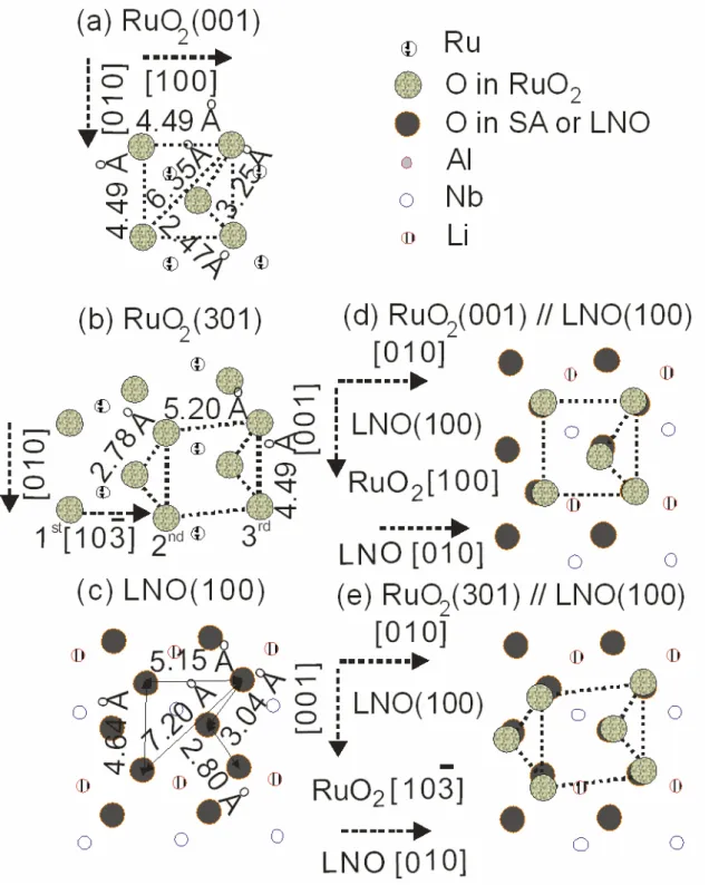
19 Liao, P. C., C. A. Chen, J. G. Chi, Y. S. Huang, D. S. Tsai, and K. K. Tiong, “Growth and structural characterization of well aligned RuO2 nanocrystals on LiNbO3 (100) via MOCVD,” J.
Alloy. Compd., DOI:10.1016/j.jallcom.2008.09.205.
We report the preparation of well aligned RuO2 nanocrystals (NCs) on LiNbO3(100) by metal organic chemical vapor deposition (MOCVD) using bis(ethylcyclopentadienyl) ruthenium (II) as the source reagent. The surface morphology and structural properties of the as-grown NCs were characterized by using field emission scanning electron microscopy (FESEM) and X-ray diffractometry (XRD). The growth pattern initiated with nucleation of both (001) and (301) planes at the substrate surface, but eventually NCs with (001) growth plane outgrew and formed a vertically aligned NCs on top of the mixed alignments at the interface. The observed
IX
epitaxial growth patterns are explained in terms of the relationship between the atomic arrangements of the substrate and the NCs and the c-directional growth mechanism.
20 Chen, C. A., K. Y. Chen, Y. S. Huang, D. S. Tsai, K. K. Tiong, and F. Z. Chien, “X-ray diffraction and Raman scattering study of thermal-induced phase transformation in vertically-a ligned TiO2 nanocrystals grown on sapphire(100) via metal organic vapor deposition,” J. Cryst.
Growth, Vol. 310, pp. 3663~3667 (2008).
We report a detailed study of thermal-induced phase transformation in TiO2 nanocrystals (NCs) via X-ray diffraction (XRD) and Raman scattering (RS) spectroscopy. Vertically-aligned anatase TiO2(110) NCs are grown on sapphire (SA)(100) substrate at 550
°C by metal-organic chemical vapor deposition, using titanium-tetraisopropoxide (TTIP, Ti[OCH(CH3)2]4) as the source reagent.
The effects of thermal annealing of TiO2 NCs in oxygen atmosphere between 600 and 1000 °C are investigated. XRD and RS spectra show the onset of the phase transformation process from the as-grown anatase TiO2(110) NCs into rutile TiO2(001) at the annealing temperature of 800 °C. At annealing temperature higher than 900 °C, pure rutile phase of TiO2(001) NCs are formed and the crystalline quality of TiO2 NCs can be further improved upon higher annealing temperature.
21 Chen, C. A., A. Korotcov, Y. M. Chen, Y. S. Huang, D. S. Tsai, K. K. Tiong, and P. C. Liao,
“Growth and characterization of vertically aligned densely packed TiO2 nanocrystals on sapphire(100) via metal-organic chemical vapor deposition,” ECS Transactions, Vol.11, pp. 19~25.
(2008).
Vertically aligned anatase- and rutile-phase TiO2 nanorods (NRs) have been grown by metal-organic chemical vapor deposition (MOCVD) on sapphire (SA)(100) substrates under different conditions, using titanium-tetraisopropoxide (Ti(OC3H7)4) as a source reagent. The surface morphology, structural and spectroscopic properties of the as-deposited NCs were characterized in detail using field emission scanning electron microscopy (FESEM), transmission electron microscopy (TEM), X-ray diffractometry (XRD) and micro-Raman scattering. FESEM and TEM micrographs reveal the growth of vertically aligned NRs on SA(100) substrates. The XRD results indicate that the anatase- and rutile-TiO2 NRs are, respectively, (110) and (001) oriented on SA(100).
Raman spectra show that pure anatase- and rutile- phase have been deposited. The roles of different growth conditions in the formation of different phases of the vertically aligned TiO2 NRs are studied and the probable mechanisms have been discussed.
22 Chen, C. A., Y. M. ChenA. Korotcov, Y. S. Huang, D. S. Tsai, and K. K. Tiong, “Growth and characterization of well-aligned rutile TiO2 nanorods on sapphire substrates via metal-organic chemical vapor deposition,” Nanotechnology, Vol. 19, 075611 (2008).
Self-assembled and well-aligned rutile TiO2 nanorods (NRs) have been grown on sapphire (SA) (100) AND (012) substrates via metal-organic chemical vapor deposition (MOCVD), using titanium-tetraisopropoxide (TTIP, Ti(OC3H7)4) as a source reagent. The surface morphology as well as structural and spectroscopic properties of the as-deposited NRs were characterized using field- emission scanning electron microscopy (FESEM), transmission electron microscopy (TEM), selected-area electron diffractometry (SAED), X-ray diffraction (XRD), and micro-Raman spectroscopy. FESEM micrographs reveal that vertically aligned NRs were grown on SA(100), whereas the NRs on the SA(012) were grown with a tilt angle of ~33° from the normal to substrates. TEM and SAED measurements showed that the TiO2 NRs on SA(100) with square cross section have long axis directed along the [001]
direction. The XRD results reveal TiO2 NRs with either (002) orientation on SA(100) substrate or (101) orientation on SA(012) substrate. A strong substrate effect on the alignment of the TiO2 NRs growth has been demonstrated and the probable mechanism for the formation of these NRs has been discussed. Micro-Raman spectrum shows the red-shift and peak broadening of the TiO2
signatures with respect to that of the bulk counterparts can be attributed to both the size and residual stress effects.
23 Chen, C. A., A. Korotcov, Y. S. Huang, D. S. Tsai, and K. K. Tiong, “Growth and characterization of well-aligned titanium dioxide nanocrystals via metal organic vapor deposition,”
Journal of Materials Science: Materials in Electronics, DOI:10.1007/s10854-008-9595-3.
Raman spectroscopy (RS) was used to study the phase transformations of nanocrytalline TiO2 thin films. The films were grown by a vertical-flow cold-wall metal organic chemical vapour deposition system, using Ti(C10H14O5) as the source reagent, at different substrate temperatures. The results indicate that the anatase phase is present at around 550 ºC and the rutile phase starts to form at 650 ºC. The anatase phase completely transforms into the rutile phase at 680 ºC. We have demonstrated that RS can be used as a powerful nondestructive technique for a quick and efficient determination of the phase of TiO2 thin films.
24 Chen, C. A., A. Korotcov, Y. S. Huang, W. H. Chung, D. S. Tsai, and K. K. Tiong, “Raman scattering study of the phase transformation on nanostructured titania prepared via metal organic
X
vapor deposition,” Journal of Materials Science: Materials in Electronics, DOI:10.1007/s10854- 008-9611-7.
Well-aligned TiO2 nanocrystals (NCs) were prepared by metalorganic chemical vapour deposition on sapphire (SA) (100) and (012) substrates, using Ti[OCH(CH3)2]4 as precursor. The surface morphology, structural and spectroscopic properties of the deposited NCs were characterized using field emission scanning electron microscopy (FESEM), X-ray diffractometry (XRD) and Raman spectroscopy (RS). FESEM micrographs show that the NCs on SA(100) are vertically aligned. XRD determines the preferable orientations of the as-deposited NCs. RS confirms rutile phase of the NCs. The roles of substrate orientations for the formation of different textures of TiO2 NCs are discussed.
25 Korotcov, A., R. S. Chen, H. P. Hsu, Y. S. Huang, D. S. Tsai, and K. K. Tiong, “Well-aligned IrO2 nanocrystals,” Journal of Nanomaterials, DOI:10.1155/2007/84845.
We review the results of synthesis of well-aligned IrO2 nanocrystals (NCs) on sapphire (SA), LiNbO3 (LNO), LiTaO3 (LTO) substrates via reactive magnetron sputtering and metal-organic chemical vapor deposition. The surface morphology and structural properties of the as-deposited NCs were characterized. Field emission scanning electron microscopy micrographs reveal that NCs grown on SA(100)/LNO(100) are vertically aligned, while the NCs on SA(012)/LTO(012) and SA(110) contain singly and doubly tilted alignments, respectively, with a tilt angle of ∼35∘ from the normal to the substrates. NCs grown on SA(001) show in-plane alignment with mosaic structure. The X-ray diffraction results indicate that the NCs are (001), (101), and (100) oriented on SA(100)/LNO(100), SA(012)/LTO(012)/SA(110), and SA(001) substrates, respectively. A strong substrate effect on the alignment of the IrO2 NCs deposition has been demonstrated. The roles of different substrates in the formation of various textures of nanocrystalline IrO2 are studied and the possible mechanisms have been discussed.
26 Korotcov, A., Y. S. Huang, K. K. Tiong, and D. S. Tsai, “Raman scattering characterization of well aligned RuO2 and IrO2 nanocrystals,” J. Raman Spectrosc., Vol. 38, pp.737~749 (2007).
Raman spectroscopy (RS) has been used as a technique for the characterization of well-aligned IrO2 and RuO2 nanocrystals (NCs) grown on a number of different oriented substrates under various conditions. The IrO2 and RuO2 NCs were grown via etalorganic chemical vapor deposition and reactive magnetron sputtering. The relative intensity of the three strongest Raman-active modes, namely, the A1g, B2g and Eg modes, depends on the orientation of NCs and has been used to determine the preferred growth irection of the NCs. The redshifts and asymmetric linewidth broadening of the Raman features of IrO2 and RuO2 NCs with respect to that of their bulk counterparts were analyzed by a modified spatial correlation (MSC) model, which includes a factor of stress-induced shift.
The MSC model showed that the effects of stress and nanometric size could be separated in analyzing the observed Raman features.
The usefulness of experimental RS together with theMSC model analysis as a structural and residual stress haracterization technique for NCs has been demonstrated.
27 Korotcov, A., H. P. Hsu, Y. S. Huang, P. C. Liao, D. S. Tsai, and K. K. Tiong, “Deposition and characterization of 1-D RuO2 nanocrystals by reactive sputtering,” J. Alloys and Compounds, Vol.
442, pp.310~312 (2007).
Well-aligned 1D RuO2 nanocrystals (NCs) have been grown on sapphire (SA)(1 0 0), SA(0 0 1) and LiNbO3 (LNO)(1 0 0) substrates via reactive magnetron sputtering using a Ru metal target. The surface morphology, structural and spectroscopic properties of the as-deposited NCs are characterized using field-emission scanning electron microscopy (FESEM), X-ray diffraction (XRD), and micro-Raman spectroscopy (RS). FESEM micrographs show that NCs grown on SA(1 0 0)/LNO(1 0 0) are vertically aligned, while NCs grown on SA(0 0 1) show in-plane alignment with mosaic structure. The XRD results indicate that the NCs are (0 0 1) and (1 0 0) oriented on SA(1 0 0)/LNO(1 0 0) and SA(0 0 1) substrates, respectively. A strong substrate effect on the alignment of the RuO2 NCs deposition has been observed and the probable mechanism for the formation of these NCs has been discussed. The usefulness of the Raman spectroscopy as a structural characterization technique of NCs has been demonstrated.
28 Liao, P. C., A. Korotcov, C. W. Huang, Y. S. Huang, D. S. Tsai and K. K. Tiong, “Synthesis of IrO2 nanocrystals on sapphire via metal-organic chemical vapor deposition,” J. Alloys and Compounds, Vol. 442, pp.313~315 (2007).
We report the results of the synthesis of IrO2 nanocrystals (NCs) on sapphire (SA) substrates with different orientations via metal- organic chemical vapor deposition (MOCVD) using (MeCp)(COD)Ir as the source reagent. The surface morphology and structural properties of the as-deposited NCs were characterized using field emission scanning electron microscopy (FESEM), and X-ray diffractometry (XRD). FESEM micrographs reveal that vertically aligned NCs were grown on SA( 1 0 0), the NCs on SA(0 1 2) and SA( 1 1 0) contained, respectively, single- and double-aligned directions with a tilt angle of 35° from the normal to the substrates, while NCs parallel in-plane alignment were gown on SA(00 1). The XRD results indicate that the IrO2NCs are (001), (101), and (1 00) oriented on SA(1 00), SA(0 1 2)/SA(1 10) and SA(00 1) substrates, respectively. A strong substrate effect on the alignment of the IrO2 NCs growth has been demonstrated and the probable mechanism for the formation of the NCs is discussed.
XI
29 Chen, Y. M., A. Korotcov, H. P. Hsu, Y. S. Huang, and D. S. Tsai, “Raman scattering characterization of well-aligned RuO2 nanocrystals deposited on sapphire substrates by reactive magnetron sputtering,” New Journal of Physics, Vol. 9, 130 (2007).
Raman scattering (RS) spectroscopy is a popular measurement technique that uses inelastic scattering of monochromatic light to study vibrational characteristics of a material system. A typical application of RS is for material structure determination. This paper describes the application of RS for the characterization of the preferable growth direction of well-aligned nanocrystals (NCs) deposited on sapphire substrates. The results indicate that RS could become a powerful technique for the quick determination of the NCs orientation. The redshifts and asymmetric linewidth broadening of the Raman features of RuO2 NCs are analysed by a modified spatial correlation (MSC) model, which includes the factor of stress-induced shift. The usefulness of experimental RS together with the MSC model analysis as a nondestructive structural and residual stress characterization technique for NCs has been demonstrated.
30 Shan, C. C., D. S. Tsai, Y. S. Huang, S. H. Jian, and C. L. Cheng, “Pt-Ir-IrO2NT thin- wall electrocatalysts derived from IrO2 nanotubes and their catalytic activities in methanol oxidation,” Chemistry of Materials, Vol.19, pp. 424~431 (2007).
The structural features and catalytic activities of PtIr electrocatalysts derived from vertical IrO2 nanotubes (IrO2NT) of 1100 nm in height and 80-100 nm in diameter have been studied using scanning electron microscopy, transmission electron microscopy, X-ray powder diffraction, and cyclic voltammetry toward COad and methanol oxidation. Lattice oxygen of IrO2NT is removed under high- vacuum thermal annealing to facilitate nucleation of 3-5 nm Ir grains and subsequent synthesis of PtIr catalyst on the tube walls.
Interestingly, the apparent dimensions and orientation of IrO2NT can be preserved via pore generation in the oxygen removal process. The tubular wall was transformed from a thin dense plate of IrO2(110) single crystal into a porous plate consisting of connected Ir grains that exhibit lattice fringes of the Ir{110} spacing with preferential orientation of Ir[110] parallel to the IrO2NT growth direction. The amount of Ir being reduced, the Ir grain size, and the deposited Pt size strongly influence the surface area and the catalytic activity. The Pt-Ir-IrO2NT catalyst reduced at 500 °C exhibits a significantly higher activity than Pt-IrO2NT and Pt- IrNT in methanol oxidation and also a higher current density than that of a Johnson-Matthey PtRu catalyst in the high potential region.
31 Chao, T. W., C. J. Liu, A. H. Hsieh, H. M. Chang, Y. S. Huang, and D. S. Tsai, “Quartz crystal microbalance sensor based on nanostructured IrO2,” Sensors and Actuators B- Chemistry, Vol.122, pp. 95~100 (2007).
Nanostructured IrO2 crystals are grown on a gold-coated quartz substrate by metal organic chemical vapor deposition (MOCVD), and their gas sensing properties are studied by quartz crystal microbalance (QCM) technique. Several morphologies, such as nanoblade, layered-column, incomplete-nanotube and square-nanorod, are observed at various combinations of substrate temperature and precursor reservoir temperature. Propionic acid is found to be adsorbed and desorbed reversibly on the IrO2
surface at room temperature, and the adsorption property depends on the nanostructure of the IrO2. IrO2 crystals with nanoblade and layered-column morphologies show higher sensitivities to propionic acid than those with incomplete-nanotube and square- nanorod morphologies. An IrO2 QCM sensor sensitive to ppm-level propionic acid vapor at room temperature is demonstrated.
32 Tsai, H. M., P. D. Babu, C. W. Pao, J. W. Chiou, J. C. Jan, K. P. Krishna Kumar, F. Z.
Chien, W. F. Pong, M. H. Tsai, C. H. Chen, L. Y. Jang, J. F. Lee, R. S. Chen, Y. S.
Huang, and D. S. Tsai, “Comparison of electronic structure of RuO2 and IrO2 nanorods investigated by x-ray absorption and scanning photoelectron microscopy,” Appl. Phys.
Lett., Vol.90, 042108 (2007).
Electronicstructures of the nanorods of RuO2 and IrO2 metallic oxideswere investigated by x-ray absorption near-edge structure (XANES) and scanningphotoelectron microscopy (SPEM). O K-, Ru, and Ir L3-edge XANESresults reveal that hybridization between O 2p and metal t2gorbitals is weaker in IrO2 than in RuO2. The enhancementof the tip-region SPEM intensities relative to those in thesidewall regions for both RuO2 and IrO2 nanorods is foundto extend over a large energy range in contrast tothose of carbon nanotubes and ZnO nanorods, which are confinedto deep below and near the Fermi level, respectively.
33 Korotcov, A., H. P. Hsu, Y. S. Huang, and D. S. Tsai, “Raman scattering characterization of well aligned IrO2 nanocrystals grown on sapphire substrates via reactive sputtering,” J. Raman
XII
Spectrosc., Vol.37, pp.1411~1415 (2006).
Raman spectroscopy (RS) was used for the characterization of well-aligned IrO2 nanocrystals (NCs) grown on sapphire substrates with different orientations via reactive magnetron sputtering. Three Raman-active modes, Eg, B2g and A1g, were observed in the range 500-800 cm-1. The intensity of certain modes depended on the orientation of NCs and followed the selection rules reasonably well. The result indicates the possibility of determining the preferred growth direction of NCs using RS. Raman spectra show red shifts and peak broadening of the IrO2 signatures with respect to those of the bulk counterpart. The red shifts and asymmetric broadening of the Raman line shapes of the NCs were analyzed by a modified spatial correlation (MSC) model, which included a factor of stress-induced shift. The MSC model showed that the effects of stress and nanometric size could be separated by analyzing the observed Raman features. The usefulness of experimental RS together with the MSC model analysis as a structural and residual stress characterization technique for NCs is demonstrated.
34 Korotcov, A., Y. S. Huang, D. S. Tsai, and K. K. Tiong, “Growth and characterization of high densely packed RuO2 nanocrystals on oxide substrates via reactive sputtering,” Crystal Growth and Design, Vol. 6, No. 11, pp. 2501~2506 (2006).
Well-aligned, densely packed RuO2 nanocrystals (NCs) have been grown on sapphire (SA), LiNbO3 (LNO), and LiTaO3 (LTO) substrates with different orientations via reactive magnetron sputtering using a Ru metal target. The surface morphology and structural and spectroscopic properties of the as-deposited NCs are characterized using field-emission scanning electron microscopy (FESEM), X-ray diffraction (XRD), X-ray photoelectron spectroscopy (XPS), and micro-Raman spectroscopy (RS). FESEM micrographs reveal that NCs grown on SA(100)/LNO(100) are vertically aligned, whereas the NCs on SA(012)/LTO(012) and SA(110) contain singly and doubly tilted alignments, respectively, with a tilted angle of _35° from the normal to the substrates. NCs grown on SA(001) show in-plane alignment with the mosaic structure. The XRD results indicate that the NCs are (001), (101), and (100) oriented on SA(100)/LNO(100), SA(012)/LTO(012)/SA(110), and SA(001) substrates, respectively. A strong substrate effect on the alignment of the RuO2 NCs deposition has been demonstrated. XPS analyses reveal the coexistence of higher oxidation states of Ru in the as-deposited RuO2 NCs. The Raman spectra show the red-shift and asymmetric peak broadening of the RuO2
signatures with respect to that of the bulk counterpart, which are attributed to both the size and residual stress effects, whereas the intensity of certain modes follows the selection rules for the different oriented NCs.
35 Korotcov, A., Y. S. Huang, T. Y. Tsai, D. S. Tsai, and K. K. Tiong, “Effect of length, spacing andmorphology of vertically aligned RuO2 nanostructures on field emission properties,”
Nanotechnology, Vol.17, pp. 3149~3153 (2006).
The length, spacing and morphology of vertical aligned nanostructural RuO2 one-dimensional (1D) arrays are varied independently to investigate their effect on the field-emission properties. It is shown that, in general, the lowest turn-on field, highest emission current density and apparent field enhancement factor can be achieved in nanocrystals (NCs) with the smallest emitter radius for the tips and the highest aspect ratio. Moreover, the lower-density NCs exhibit better field-emission characteristics, which are related to the screening effect. The results could be valuable for the application of field-emission-based devices using RuO2 NCs arrays as cathode materials.
36 Chen, R. S., A. Korotcov, Y. S. Huang, D. S. Tsai, “One dimensional conductive IrO2
nanocrystals,” Nanotechnology, Vol.17, pp.R67~R87 (2006).
We review the results of the synthesis of IrO2 nanocrystals (NCs) on different substrates via metal-organic chemical vapour deposition (MOCVD) using (MeCp)(COD)Ir as the source reagent. The surface morphology, structural and spectroscopic properties of the as-deposited NCs were characterized using field emission scanning electron microscopy (FESEM), transmission electron microscopy (TEM), selected-area electron diffractometry (SAD), x-ray diffractometry (XRD), x-ray photoelectron spectroscopy (XPS) and Raman spectroscopy. The roles of different substrates for the formation of various textures of nanocrystalline IrO2 are studied. Several one-dimensional (1D) nanostructures have evolved by decreasing the degree of interface instability. The morphological evolution occurs from triangular/wedged nanorods via incomplete/scrolled nanotubes to square nanotubes and square nanorods (NRs), with increasing morphological stability. The results show that the three-dimensional (3D) grains composing traditional film belong to the most stable form as compared to all the ID NCs, and the sequential shape evolution has been found to be highly correlated to a morphological phase diagram based on the growth kinetics. In addition, area selective growth of IrO2NRs has been demonstrated on sapphire(012) and sapphire(100) substrates which consist of patterned SiO2 as the nongrowth surface.
The initial growth of IrO2 nuclei is studied. Selectivity, rod orientation, and other morphological features of the nanorod forest can find their origins in the nucleation behaviour during initial growth. XPS analyses show the coexistence of higher oxidation states of iridium in the as-grown IrO2 NCs. The usefulness of the experimental Raman scattering together with the modified spatial correlation (MSC) model analysis as a residual stress and structural characterization technique for ID IrO2 NCs has been demonstrated. The field emission properties of the vertically aligned IrO2 NRs are studied and demonstrated as a high-performance and robust field emitter material owing to its low work function, low resistivity and excellent stability against oxygen.
37 Wang, G., D. S. Tsai, Y. S. Huang, A. Korotcov, W. C. Yeh and D. Susanti, “Selective growth of

![Fig. 1. FESEM images of IrO 2 NCs deposited on top of TiO 2 (001) NRs: (a) 30˚ perspective view and (b) cross-sectional view images, the insets show the orientation relationship between IrO 2 [001] and the preferred orientation of (101) plane](https://thumb-ap.123doks.com/thumbv2/9libinfo/9123755.408312/42.892.274.615.125.883/fesem-deposited-perspective-sectional-orientation-relationship-preferred-orientation.webp)
![Fig. 3. (a) The TEM image of a free standing V-shaped IrO 2 NW with SAED patterns showing the junction and the arms; (b) the SAED pattern along the [010] zone axis of the junction; (c) the HRTEM images in the vicinity of the V-shaped junction regime](https://thumb-ap.123doks.com/thumbv2/9libinfo/9123755.408312/44.892.130.765.132.771/standing-patterns-showing-junction-pattern-junction-vicinity-junction.webp)
