國 立 交 通 大 學
電子工程學系 電子研究所碩士班
碩 士 論 文
一個
一個
一個
一個 10GHz 快速鎖定之全數位式頻率合成器
快速鎖定之全數位式頻率合成器
快速鎖定之全數位式頻率合成器
快速鎖定之全數位式頻率合成器
A 10GHz, Fast-Locking All-Digital Frequency
Synthesizer
研 究 生 : 楊松諭
指導教授 : 陳巍仁
一個
一個
一個
一個 10GHz 快速鎖定之全數位式頻率合成器
快速鎖定之全數位式頻率合成器
快速鎖定之全數位式頻率合成器
快速鎖定之全數位式頻率合成器
A 10GHz, Fast-Locking All-Digital Frequency
Synthesizer
研 究 生:楊松諭 Student : Song-Yu Yang
指導教授:陳巍仁 Advisor : Wei-Zen Chen
國立交通大學
電子工程學系 電子研究所 碩士論文
A Thesis
Submitted to Department of Electronics Engineering and Institute of Electronics College of Electrical and Computer Engineering
National Chiao-Tung University in Partial Fulfillment of the Requirements
for the Degree of Master
in
Electronics Engineering November 2008
Hsin-Chu, Taiwan, Republic of China
i
一個
一個
一個
一個 10GHz 快速鎖定之全數位式頻率合成器
快速鎖定之全數位式頻率合成器
快速鎖定之全數位式頻率合成器
快速鎖定之全數位式頻率合成器
研究生: 楊松諭 指導教授:陳巍仁教授國立交通大學
電子工程學系電子研究所碩士班
摘要
摘要
摘要
摘要
本論文提出一個具有動態迴路濾波器的 10GHz 快速鎖定之全數位式頻 率合成器。其中,動態迴路濾波器主要由一個鎖定追蹤監測器(Locking Process Monitor, LPM)控制,可在追蹤相位時自動調整迴路濾波器的參數, 使得整體迴路頻寬可自動調整直到頻率鎖定。利用此機制可使得整體鎖定 時間低於 8µs,且當輸出頻率為 9.92GHz 時,其抖動(jitter)的均方根低於 1 ps。在此論文中,並提出一個具偏斜補償的相位累加器電路,使其不只能夠 在高速下運作,亦可有低功率的優勢。此論文中的晶片是使用 90nm CMOS 技術實現,整體晶片面積為 0.902mm2,核心電路的部份只佔 0.352mm2,使 用電壓為 1V,消耗功率約 7.1 mW,其中數位輸入/輸出單元的電壓為 3.3V, 消耗功率為 2.7 mWii
A 10GHz, Fast-Locking All-Digital Frequency Synthesizer
Student: Song-Yu Yang Advisor: Wei-Zen Chen
Department of Electronics Engineering & Institute of Electronics
National Chiao-Tung University
Abstract
A 10 GHz all digital frequency synthesizer with dynamic digital loop filter is presented. Governed by a locking process monitor (LPM), the digital loop filter is automatically reconfigured during the frequency acquisition and phase tracking process. Also, the loop bandwidth is self-adjusted to a moderate bandwidth as the loop settles to phase and frequency lock. With less than 8 µsec locking time, the measured rms jitter from a 9.92 GHz carrier is less than 1 ps. A skew-compensated phase accumulator is proposed for high speed operation, which preserves the advantages of low power dissipation while eliminating the accumulated timing skew issue. Implemented in a 90 nm CMOS technology, the core area is only 0.352 mm2, and the chip size including bonding pad is 0.902mm2. The ADPLL core consumes 7.1 mW from a 1V supply, and the digital I/O cells drains 2.7 mW from a 3.3V supply for chip measurement.
iii
Acknowledgement
歷經四年的時間,從一開始連 PLL 是什麼都搞不清楚,到這本論文的 完成,實在很感謝我的指導教授,陳巍仁老師的帶領。在此過程,無論是 在專業領域以及待人處世,都讓我受益匪淺。 在這段漫長的研究生涯,特別感謝本實驗室金牌-台祐學長、在工作的 大建文和岱原學長,唯有你們的幫助,才有本論文的誕生。也感謝 lulu 裕、 黃董、小神童、國忠、順哥、晏維、鯉魚、科科、塔哥、宗恩、歐大大、 歐陽、國維、小州哥、阿宅、小凡、邱 99、小賴、彥緯、育祥、順天、Kitty、 新爺、還有本實驗室的新血書謹、旻毅、文杰、健軒、郭老師實驗室的同 學與學弟…等。由於你們的陪伴以及幫忙,帶給我許多的方便以及快樂的 回憶,祝福你們未來在工作或學業上都能夠一路順風,而還沒畢業的學弟 妹能早日畢業。 另外,我也特別感謝我的閃光-巧伶和在背後默默支持我的家人,在這 段期間的對與我的關懷和付出。最後,感謝主,讓我能夠順利的畢業了! 楊松諭 17, Nov, 2008iv
Contents
摘要 摘要 摘要 摘要 ... i Abstract ...ii Acknowledgement ...iii Contents... ivList of Tables ...vii
List of Figures ...viii
Chapter 1 Introduction ... 1
1.1 Motivation ... 1
1.1.1 Introduction of Frequency Synthesizers ... 1
1.1.2 Target Application and its Requirements ... 4
1.2 Overview of Thesis... 5
Chapter 2 ADPLL Architecture ... 7
2.1 Architecture of BBPLL ... 7
2.1.1 Analog PLL ... 7
2.1.2 All-Digital PLL ... 9
2.2 Proposed Solution... 11
2.2.1 Proposed Dual Mode ADPLL Architecture ... 11
2.2.2 Overview of the Operation... 12
2.2.3 Dynamic Loop-Gain Control ... 14
Chapter 3 Analysis of the ADPLL ... 18
3.1 ADPLL in Frequency Acquisition Mode ... 18
3.2 ADPLL in Phase Tracking Mode ... 22
3.2.1 Locking Transient of the ADPLL during Phase Tracking Mode 22 3.2.2 Stability Conditions of the ADPLL during PT Mode ... 28
3.2.3 Locking Range of the ADPLL during PT Mode... 28
v
3.2.5 Input jitter tolerance of the ADPLL during PT Mode... 36
3.3 Output Noise Performance of the ADPLL ... 37
3.3.1 Output Spur ... 38
3.3.2 The Linear Model of the ADPLL during PT Mode ... 40
3.3.3 Generated Timing Jitter and Phase Noise ... 46
Chapter 4 Design and Implementation of the ADPLL ... 55
4.1 Block Diagram of the ADPLL... 55
4.2 Phase Detection Circuits ... 57
4.2.1 Modulo arithmetic of the phase detection circuit ... 59
4.2.2 PAC2 ... 62
4.3 Digital Loop Filter and LPM... 70
4.4 Digital Controlled Oscillator (DCO)... 75
4.4.1 Varactor Banks ... 77
4.4.2 Inductor Coil ... 84
4.4.3 Simulation results of DCO ... 85
4.5 Divided-by-4 Prescaler... 87
Chapter 5 Experimental Results ... 90
5.1 IC Chip ... 90
5.2 Evaluation Board ... 91
5.3 Measurement Setup ... 93
5.4 DCO Measurement Results ... 94
5.4.1 DCO Tuning Curve ... 94
5.4.2 Open loop DCO phase noise... 98
5.5 Closed-Loop Performance... 99
5.5.1 Output Spectrum ... 99
5.5.2 Output Phase Noise ... 101
5.5.3 Jitter Performance ... 103
5.6 Locking Behavior ... 107
5.7 Performance Summary ... 109
vi
Reference ... 112 Vita... 115
vii
List of Tables
Table 4-1 Tuning characteristics of the DCO... 85
Table 4-2 Tuning characteristics of the DCO... 87
Table 5-1 Summary of the power consumption ... 109
viii
List of Figures
Fig. 1-1 Block diagram of a phase-locked loop ... 2
Fig. 1-2 Block diagram of optical transmitter and receiver. ... 4
Fig. 2-1 Typical charge-pump-based PLL... 7
Fig. 2-2 Block diagram of the ADPLL architecture proposed in [3] ... 9
Fig. 2-3 Block diagram of the digital BBPLL architecture proposed in [4]. ... 11
Fig. 2-4 Block diagram of the proposed ADPLL... 12
Fig. 2-5 Frequency detection by edge counting... 13
Fig. 2-6 Equivalent frequency locked loop during FA mode... 13
Fig. 2-7 Equivalent Block diagram of the ADPLL during PT mode. ... 14
Fig. 2-8 The block diagram of LPM and its time diagram. ... 16
Fig. 2-9 Simulated locking behavior with and without LPM for the same steady state loop bandwidth (100 kHz). ... 17
Fig. 3-1 System block diagram during frequency acquisition mode. ... 18
Fig. 3-2 Equivalent system block diagram during frequency acquisition mode. 19 Fig. 3-3 (a) Pole-zero plot and (b) the damping factor as a function of KFA of the ADPLL during frequency acquisition mode ... 20
Fig. 3-4 Simulated time domain response of the ADPLL in frequency acquisition mode with 3 different KFA value. ... 20
Fig. 3-5 System block diagram during bang-bang phase tracking mode... 23
Fig. 3-6 Equivalent system block diagram during bang-bang phase tracking mode. ... 23
Fig. 3-7 (a) Simulated output frequency, (b) phase error versus time and (c) the phase plane of the BBPLL. ... 25
Fig. 3-8 Time diagrams of the signals in the BBPLL (Adapted from [7])... 26
Fig. 3-9 Simulated locking behavior of BBPLL with (a) constant delay (D=0.5) and (b) constant α and β (α=1, β=8)... 29
Fig. 3-10 The locking transient of the BBPLL. ... 30
Fig. 3-11 Phase plane illustrating the boundary used to derive the locking range. ... 31
Fig. 3-12 Allowed maximum initial frequency error versus loop parameters KDCOα and KDCOβ for BBPLL. ( fREF=40MHz, N=248, D=0.5, and υ=8.) .. 33
Fig. 3-13 Trajectory plot for the computation of the locking time. (Adapted from [7]) ... 34 Fig. 3-14 Simulation result of DCO output frequency versus time during locking
ix
process of BBPLL. (∆f0=6MHz, KDCO=20kHz, α=1, β=32, D=0.5 and
fREF=40MHz.) ... 35
Fig. 3-15 Maximum input noise power sufficient to cause slew-limiting as a function frequency and with KDCOα as a parameter. ... 37
Fig. 3-16 (a) The simulation results of the output frequency versus time and (b) the output spectrum in locked state of the ADPL with the following parameters: fREF=40MHz, α=1, β=128, KDCO=500, D=0.5 and N=248. ... 39
Fig. 3-17 BPD linearized model... 41
Fig. 3-18 State chain to approximating the BBPLL... 43
Fig. 3-19 (a) Discrete time model and (b) continuous time approximation of the digital loop filter. ... 45
Fig. 3-20 Complete linearized model of the ADPLL during bang-bang phase tracking mode. ... 46
Fig. 3-21 Simplified linearized model of the ADPLL during bang-bang phase tracking mode with internal and external noise sources. ... 47
Fig. 3-22 Example computation of ADPLL transfer functions and contribution of each noise source... 51
Fig. 3-23 Output phase noise with KDCOα=3×10 2 and KDCOβ=3.84×10 4 ... 51
Fig. 3-24 Output phase noise with KDCOα=3×10 2 and KDCOβ=7.68×10 4 ... 52
Fig. 3-25 Output phase noise with KDCOα=3×10 2 and KDCOβ=3.07×10 5 ... 52
Fig. 3-26 Output phase noise with KDCOα=3×10 2 and KDCOβ=4.9×10 6 ... 52
Fig. 3-27 Output phase noise with KDCOα=4.8×10 3 and KDCOβ=7.68×10 4 ... 53
Fig. 3-28 Output phase noise with KDCOα=1.92×10 4 and KDCOβ=7.68×10 4 ... 53
Fig. 3-29 Output jitter versus KDCOβ and KDCOα... 54
Fig. 4-1 Block diagram of the implemented ADPLL ... 56
Fig. 4-2 Block diagram of the phase detector ... 58
Fig. 4-3 Behavior model of υ-bit accumulator... 59
Fig. 4-4 Simplified block diagram of phase detector. ... 60
Fig. 4-5 Rotating vector interpretation of the reference and feedback phases. .. 61
Fig. 4-6 Asynchronous counter. ... 63
Fig. 4-7 Synchronous counter. ... 64
Fig. 4-8 Example of a 1-bit counter with sample phase generator. ... 66
Fig. 4-9 Example of a 1-bit counter with an additional D type flip-flop... 67
Fig. 4-10 Bock diagram and time diagram of the proposed high speed counter.68 Fig. 4-11 Schematic of the tactical flip flop [13] ... 69
Fig. 4-12 Implementation of the digital loop filter... 71
Fig. 4-13 Implementation of the gain controller ... 72
x
Fig. 4-15 Implementation of the LPM. ... 73
Fig. 4-16 Flowchart of the ADPLL locking process. ... 74
Fig. 4-17 Implemented block diagram of DCO system. ... 76
Fig. 4-18 Gate capacitance v.s. drain and source voltage, VC, of a simulated NMOS varactor with L=0.08µm, W=0.16µm... 78
Fig. 4-19 DCO quantization noise model. ... 79
Fig. 4-20 Phase noise due to frequency quantization of different frequency resolution step... 80
Fig. 4-21 Phase noise due to Σ∆-shaped frequency quantization with different dithering frequency... 81
Fig. 4-22 Phase noise due to Σ∆-shaped frequency quantization with different order of Σ∆ modulator. ... 82
Fig. 4-23 Schematic of the fine tune cell shown in Fig. 4-17... 83
Fig. 4-24 Block diagram of the 2nd MASH-II order Σ∆ modulator. ... 84
Fig. 4-25 The layout view (a) and the EM simulation results (b) of the inductor. ... 84
Fig. 4-26 Simulated phase noise performance of the DCO. ... 85
Fig. 4-27 Simulated time domain waveform of the DCO... 86
Fig. 4-28 Schematic of the divided-by-2 frequency divider [13]. ... 87
Fig. 4-29 Simulated time domain waveform of the divided-by-4 prescaler. ... 88
Fig. 5-1 Chip photograph of the implemented ADPLL. ... 90
Fig. 5-2 (a)AC PCB and (b)DC PCB for evaluating the chip... 91
Fig. 5-3 GUI program for controlling the chip ... 92
Fig. 5-4 Measurement setup of the test chip. ... 93
Fig. 5-5 Measured DCO frequency versus control code of coarse tuning bank CDCO[24:18]. ... 95
Fig. 5-6 Measured DCO frequency versus control code of fine tuning bank CDCO[17:8]. ... 96
Fig. 5-7 Measured DCO frequency step versus control code of Σ∆ bank CDCO[17:8]. ... 96
Fig. 5-8 Measured DCO frequency versus control code of Σ∆ bank CDCO[7:0]. 97 Fig. 5-9 Measure open loop phase noise from 9.98GHz carrier. ... 98
Fig. 5-10 Measured synthesizer output spectrum of 9.92GHz carrier with α=1 and β=256. ... 99
Fig. 5-11 Measured synthesizer output spectrum of 10.08GHz carrier with α=1 and β=256. ... 100
Fig. 5-12 Output spectrum of β=64,256 and 1024... 101
xi
Fig. 5-14 Measured phase noise for 9.92GHz output with α=1 and β=256. .... 102
Fig. 5-15 Measured phase noise for 4 different loop filter setting... 103
Fig. 5-16 Measured output waveform from 9.92GHz carrier with α=1 and β=256. The rms jitter is 904fs... 104
Fig. 5-17 Measured output waveform from 9.92GHz carrier with α=1 and β=512. The rms jitter is 890fs... 105
Fig. 5-18 Measured output waveform from 10.08GHz carrier with α=1 and β=256. The rms jitter is 1001fs. ... 105
Fig. 5-19 Measured output waveform from 10.08GHz carrier with α=1 and β=512. The rms jitter is 998fs. ... 106
Fig. 5-20 Measured rms jitter from 9.92GHz carrier with constant α and different β values. ... 106
Fig. 5-21 The measured settling time for the output frequency changes from 9.92GHz to10.08GHz (divided-by-8 clock changes from 1.24GHz to 1.26GHz). ... 107
Fig. 5-22 Zoomed in version of the measured settling behavior. ... 108
Fig. 5-23 The measured DCO control code during frequency hopping. ... 108
1
Chapter 1
Introduction
1.1
Motivation
1.1.1
Introduction of Frequency Synthesizers
Frequency synthesizers are the key building blocks for most of the modern electronic and communication systems, including radio receivers, mobile telephones, and satellite receivers. The basic goal of a frequency synthesizer is to generate a periodic signal with a given frequency and phase relationship with respect to a reference signal. The generated clock signal can be served as clock source for processors, transmit clock in high speed data interfaces, sampling clock for analog to digital convertor, and local oscillator signal for wireless transceiver which mixes the signal of interest to a different frequency. Many approaches of frequency synthesizers have been devised over the years, such as phase-locked loops (PLLs), direct digital synthesis (DDS), and frequency mixing. Among different approaches of frequency synthesizer, most state of the art high-performance frequency synthesizers are based on the phase-locked loops technique.
A phase-locked loop is a frequency control system with negative feedback. By sensing the phase difference between the feedback path of a controlled oscillator and the input reference signal, a PLL generates a signal with the phase that has a fixed relation to the phase of a reference signal. It responds to both the frequency and the phase of the reference signal and automatically raises or lowers the frequency of a controlled oscillator until output signal is matched to the reference in both frequency and phase. A PLL can be used to generate a
2
signal, modulate or demodulate a signal, reconstitute a signal with less noise, or multiply or divide a frequency.
The basic structure of a phase-locked loop is illustrated in Fig. 1-1 [1], which consists of a controlled oscillator, a phase frequency detector, a loop filter, and a feedback frequency divider. In this architecture a controlled oscillator generates a periodic signal with a frequency fOUT determined by the value of
controlled oscillator input. The output clock is divided by a feedback frequency divider having a frequency fFB=fOUT/N, where N is the divided ratio of the
frequency divider. A phase frequency detector compares the phase or frequency difference between the feedback clock and a reference clock, having a frequency fREF. The output signal of phase frequency detector which carries the frequency
or phase error information is then processed by a loop filter. The abrupt changes in the error information generated by phase frequency detector are then smoothed out by loop filter. Finally, the output of the loop filter feeds to the controlled oscillator and adjusts the frequency fOUT of the output clock. The loop
reaches a steady state condition where fOUT=fREFN, and the given relationship
between the output clock and reference clock is established if the loop is properly designed.
3
The design of the CMOS integrated PLL based RF synthesizers remains one of the most challenging tasks in communication systems because they must meet the strict requirements of low-cost, low-power, monotonic implementation while also meeting the noise and transient specifications. In general, a frequency synthesizer design can be evaluated by the following considerations: Phase noise or jitter performance, spurious noise performance, frequency hopping speed, tuning bandwidth, rejection of supply or substrate noise, chip area, power consumption and portability for the design to transfer to a different technology node. However, there exist complicated design trade-offs among these criteria mentioned above. Therefore the requirements that a synthesizer must fulfill depend heavily on the specific application.
The conventional PLL based RF synthesizer is usually made as an analog building block. As the feature size of the CMOS technology becomes smaller, the low-voltage deep-submicrometer digital CMOS process allows more and more digital circuits to be integrated in a single ship with higher operation frequency while consuming less power due to smaller parasitic capacitance and lower supply voltage. The analog circuits, however, does not benefit much from the scaling of the CMOS devices. Indeed, the small voltage headroom, high leakage current and the noisy environment on a SOC make the design of high-performance synthesizers more and more difficult. Thus, many research efforts recently focus on the digitally intensive or digitally assisted approach of the RF synthesizer [2]-[4]. Next, a description of the target application and its requirements on the synthesizer will be given.
4
1.1.2
Target Application and its Requirements
The rapidly growing volume of data transfer in telecommunication networks has motivated the widespread usage of the optical communication, which permits transmission over longer distances and at higher data rates than other forms of communication channels. Fig. 1-2 shows the block diagram of a generic optical communication system [5].
At the transmit side, the input parallel data is first converted to serial data by the serializer. Since the output of the serializer may suffer from nonidealities such as jitter and inter-symbol interference (ISI). The serial data is resampled by a flip-flop triggered by the clock multiplication unit (CMU) before the signal is sent to the laser driver. The output of retimer is then amplified to drive the laser diode. Finally, the optical signal is generated by the laser diode and guided by the optical fiber.
At the end of the fiber, a photodiode senses the light and produces electrical
5
current signal to the transimpedance amplifier (TIA). A high gain limiting amplifier (LA) follows the TIA and generates output signal with large voltage swing to provide logical levels. In order to perform synchronous operations such as retiming and deserializing on the random data, the receiver side must generate a clock. The task of generating such a clock from input data and retiming the data are performed by the clock and data recovery circuit (CDR). Finally, the original parallel data is reproduced by the deserializer.
The clock multiplication unit has been selected as our target in this thesis. In the synchronous optical network (SONET) standard, the data rate of the bitstream carried by the digital signal is defined by the optical carrier (OC) level. For example, the SONET OC-192 is a network line with transmission speeds of up to 9953.28 Mbit/s. Another major design consideration is the output jitter performance. The SONET specifications impose output peak-to-peak and rms jitter at the transmitter optical interface below 0.1UI and 0.01UI when integrated between 50 kHz and 80 MHz. These correspond to 10ps and 1ps for an OC-192 carrier. The goal of this work is to design a frequency synthesizer which generates a low jitter 10 GHz clock satisfying the SONET OC-192 specifications.
1.2
Overview of Thesis
The thesis is organized as follows. In chapter 2, the conventional analog PLL implementations and the state of the art digital frequency synthesizers will be shortly addressed with comments on systems and technology trend. The proposed all-digital phase locked loop (ADPLL) architecture and its operation principle will be presented.
6
In chapter 3, we make some investigations on the dynamic of the ADPLL. The conditions for stability and the expression of locking range will also be derived. To obtain the noise transfer function of the loop, a linear model for the ADPLL is introduced. The output phase and jitter will be analyzed with the help of the linear model.
Chapter 4 starts with the top level block diagram of the ADPLL. The implementation details of the most important building block, namely the phase detection circuits, the digitally controlled oscillator and the high speed frequency divider, will be described.
In chapter 5, the experiment setup and the measurement results of the implemented prototype will be presented. Finally, a brief conclusion of this work is given in chapter 6.
7
Chapter 2
ADPLL Architecture
2.1
Architecture of BBPLL
2.1.1
Analog PLL
A great majority of high performance analog PLL are based on the charge-pump PLL structure [5]. The structure of the charge-pump PLL is shown in Fig. 2-1. The phase frequency detector (PFD) estimates the phase difference between the reference clock fREF and the divided-by-N voltage controlled oscillator (VCO)
clock fFB by measuring the time difference between their closest edges and
generates either an Up or a Down pulse with width proportional to the time difference measured. The current pulse generated by the charge pump is converted into the control voltage of the VCO at the loop filter. The main task of the loop filter is to suppress the glitches introduced by the charge pump on every phase comparison instance. The loop automatic adjusts the VCO control voltage by the feedback mechanism, so that under locked conditions, the average output
PFD 1/N fREF fFB fOUT=fREF×N VCO Up Down Charge Pump Frequency Divider Loop Filter
8
frequency establishes an exact relationship to the reference input frequency. With proper design of the loop parameters, the performance of the charge-pump PLL can meet the requirements of different applications including Ethernet receivers, disk drive read/write channels, wireless transceivers, high-speed memory interfaces. Unfortunately, big challenges to the implementation of low-jitter analog synthesizers are coming from future system and technology trends.
The explosive growth of today’s telecommunication market has brought an increasing demand for low cost, reduced power consumption and more functionality of the silicon chip. These requirements are driving an unprecedented degree of integration of digital and analog circuitry on the same die forming what is known as System-on-Chip (SoC).
As the technology paradigm shifts into the nano-meter CMOS arena, the advanced process presents the new integration opportunities but complicates the implementation of traditional RF and analog circuits. For example, charge-pump-based PLL implementations in the deep-submicron CMOS may encounter capacitor leakage, current mismatch, and limited dynamic range under low supply voltage, leading to higher noise floor and spurious tone emission. Moreover, the high degree of integration allows more digital switching noise to be coupled into the high-precision analog section through the power supply network and the low-resistance substrate. This degrades the noise signal to noise ratio of the analog circuit and the problem gets worse with the scaling down of the supply voltage.
On the other hand, migrating to the digitally intensive frequency synthesizer can benefit from the advantages of the digital design, including robustness against process-voltage-temperature (PVT) variation and substrate
9
noise, higher flexibility of the loop filter design, fast design turnaround cycles, ease of testability, smaller silicon area and less power dissipation, which can get better with each process node. Consequently, digital intensive or digital assistance approached of the frequency synthesizers have drawn tremendous research efforts recently [2]-[4]. In next section, some of the state of the art all digital synthesizer will be illustrated.
2.1.2
All-Digital PLL
Due to the lack of the low-jitter digitally controlled oscillator (DCO), all digital PLLs really took off in practical high-performance RF applications in the past decade. Recently, a digitally controlled oscillator, which deliberately avoids any analog tuning voltage controls, was first ever presented in [2] for RF wireless applications. The phase domain ADPLL which uses this DCO is also reported in [3]. Its block diagram is shown in Fig. 2-2. Excellent phase noise performance and fine frequency resolution is achieved through the LC-tank based DCO and high-speed Σ∆ dithering. The variable phase RV[i] is determined by counting the
10
number of rising clock transitions of the DCO oscillator clock, while the reference phase RR[k] is obtained by accumulating the frequency command
word (FCW) with every rising edge of the retimed reference clock CKR. The phase error is resolved by subtracting RV[i] from RR[k] and then filtered by a
digital loop filter. Finally, the output of the filter is fed to the normalized DCO to adjust the output frequency.
Due to the edge counting nature, the quantization resolution is limited by the DCO clock period. For wireless applications, a finer resolution is required. This is achieved by using the time to digital converter (TDC), which measures the fractional time difference between the reference clock and the next rising edge of the DCO clock. It has a resolution of a single inverter delay, which is better than 40ps in the deep-submicrometer CMOS process. In order to accomplish good phase noise performance, great care must be taken with the TDC layout matching and the accuracy of the DCO period normalization factor for the output of TDC.
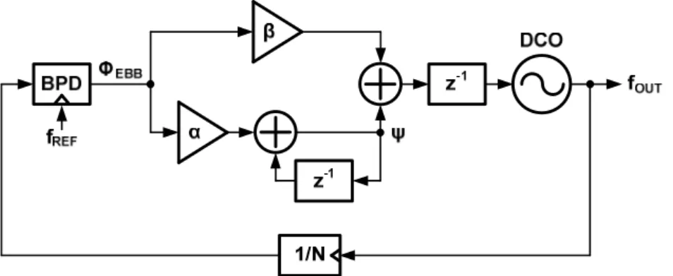
In [4] an all digital bang-bang PLL (BBPLL) with spread-spectrum capability is presented for the application of memory controller. The structure of the BBPLL is addressed in Fig. 2-3, where the phase information between the reference clock Fref and the feedback clock Fdiv is estimated by a simple binary phase detector (BPD). Its operation is equivalent to a one bit quantizer for the phase error. Since the BPD is sensitive only to the polarity of the phase information, it may suffer from long locking time with large initial frequency error.
11
According to the method of the phase sensing, the ADPLL can be roughly classified into two major categories: linear phase detection and binary phase detection. [3] is belong to linear phase detection while [4] may represent the latter one. The ADPLL with linear phase detection may resort to the TDC or more complicated phase detector design compared to the one with binary phase detector. However, its counterpart that utilizes the binary phase detection suffers from larger output jitter, higher spur energy and longer settling time.
2.2
Proposed Solution
2.2.1
Proposed Dual Mode ADPLL Architecture
The architecture of the 10GHz ADPLL is illustrated in Fig. 2-4, which is composed of a dual-mode phase frequency detector (DPD), a PI digital loop filter composed of programmable integral (α) and proportional (β) path, a locking process monitor (LPM), an LC based digital controlled oscillator (DCO), a divide-by 4 prescaler, and two phase accumulators PAC1 and PAC2. The PAC1 accumulates quarter of the frequency multiplication factor (N/4), while
12
PAC2 accumulates the prescaler output phase. The phase difference (ΦE)
between fREF and fOUT/N is then resolved by a subtracter. In the locked state, the
difference between the contents in PAC1 and PAC2 is constant. The DPD is operated in the linear mode during frequency acquisition (FA), and is turned into binary mode during the phase tracking (PT) process. In order to reduce the power consumption of PAC2, a divided-by 4 prescaler is introduced after the DCO. In the following section, the operation principle of the ADPLL will be discussed in detail.
2.2.2
Overview of the Operation
In the initial phase of the locking process, the loop starts with the FA mode. During this mode, the DPD is operated in linear mode (Mode=0) and the integral path of the digital loop filter is disabled (α=0), leading the PLL to become a second order frequency acquisition loop. To accelerate frequency acquisition, a larger forward path gain βFA1 is first applied and then switched to a smaller βFA2
after the loop is settled [15].
13
The principle of the frequency detection can be explained as following. Consider the case shown in Fig. 2-5. If M denotes the number of the rising edge appeared during a reference clock cycle, the relationship between the output frequency fOUT and the reference frequency fREF can be expressed as
REF OUT
f f
M = . (2-1)
The difference between M and the frequency multiplication factor N is
REF TARGET OUT f f f N M − = − , (2-2)
where fTARGET is the target output frequency NfREF. Thus the frequency error can
be estimated by (M-N), which can lead to the frequency locked loop as shown in Fig. 2-6. It can be shown that this architecture is equivalent to the structure
Fig. 2-5 Frequency detection by edge counting.
N fOUT + -DCO Z-1 M fREF Z-1 1 Z-1 Z-1 fREF + -Accumulator fREF Loop Filter β
14
shown in Fig. 2-4, by moving the accumulator of the loop filter before the subtracter and noting that α=0.
After ΦE variation is within 1 LSB, the LPM will launch the PT mode. The
integral path is then activated, and the whole system is turned into a 2nd order phase-locked loop. In the meantime, PAC1 and PAC2 are reset, while the content of the integrator in the loop filter (ΨI) is preset to the current DCO
control code. Afterwards, the DPD is switched to the binary phase detection mode by asserting the control signal Mode to 1 without resorting to sophisticated time to digital converter. In the mode, the DPD senses the phase difference ΦE on every reference period and generates the output bit stream to
the loop filter according to its polarity. For example, if ΦE is less than zero, DPD
outputs -1. If ΦE is equal or larger than zero, DPD outputs 1. Therefore, the loop
behavior can be simplified and described by the bang-bang PLL (BBPLL) as shown in Fig. 2-7. The term BBPLL will be used to represent the ADPLL during PT mode in this thesis.
2.2.3
Dynamic Loop-Gain Control
During PT mode, a larger β intends to broaden the loop bandwidth and speed up the locking process, but induces in larger steady state jitter. On the contrary, a
15
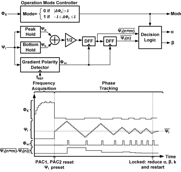
smaller counterpart can suppress the spur and reduce peak to peak jitter, but may result in a lengthy locking time and a narrower lock-in range. To overcome this trade-off, a dynamic loop gain control scheme is proposed. The α and β are adjusted under the constraint of loop stability [7], while optimizing in locking speed, timing jitter, and reference spur prospects.
According to the Σ∆ analogy in the bang-bang PLL behavior [7], the mean value of ΨI (ΨI) could represent the locking frequency of the PLL. Thus the
proximity of frequency-locked can be detected by monitoring the ripple superimposed on ΨI, which will diminish as the loop approaching the locked
state.
Based on this principle, the LPM is realized as shown in Fig. 2-8. It is composed of an operation mode controller, peak/bottom hold detectors, a gradient polarity detector (GPD), registers, and a decision logic for adjusting α and β. The LPM rapidly captures ΨI by sensing the phase error ΦE and ΨI, so
as to adjust α, β and the operation mode (FA and PT mode) accordingly. The GPD generates pulse Φsc as the slope of ΨI changes its polarity. The local
maximum (Ψp) and minimum (Ψb) of ΨI can then be updated by the peak/bottom
hold detector, which is toggled by Φsc. Without resorting to time consuming
filters, ΨI can be approximated as the average of successive peak and bottom
values
2
Ψ Ψ
ΨI ≈ p + b . (2-3)
The criterion of approaching lock (ΨI ≈constant) can be expressed as:
(
n+m)
−Ψ( )
n ≤k16
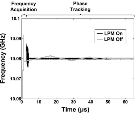
where k is the locking window and m denotes the time interval between two adjacent peak/bottom values. Under this circumstance, α, β and k are decreased to resume LPM, making the loop bandwidth being dynamically adjusted from a wide-band mode to a narrow band mode. The loop parameters, α, β and k will remain unchanged until the loop reach the next locked state again. After 5 times of the switching gain operations, the loop will finally stay with the state where the loop parameters is optimizing for low output jitter. Fig. 2-9 shows the simulated locking behavior with and without LPM for the same steady state loop
1 ∆Φ 1≤ E≤ − 1 ∆ΦE >
17
bandwidth. The simulation result shows 10 times locking speed improvement (locking time reduced from 50µs to 5µs) with the aid of the proposed scheme.
In the next chapter, the loop dynamic, and the noise performance will be analyzed.
Fig. 2-9 Simulated locking behavior with and without LPM for the same steady state loop bandwidth (100 kHz).
18
Chapter 3
Analysis of the ADPLL
3.1
ADPLL in Frequency Acquisition Mode
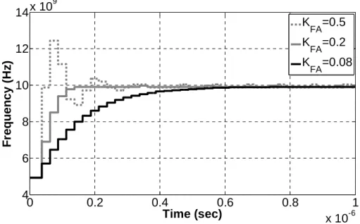
At the beginning of the locking process, the frequency acquisition mode is first activated and the DCO is locked roughly to the desired frequency. During this mode, the integral path of the digital loop filter is disabled (α=0), and the system block diagram can be simplified as shown in Fig. 3-1. The scaling factor βFA
introduced in the figure denotes the forward path gain during frequency acquisition mode. In the frequency domain it controls the gain of the frequency detected in response to the frequency changed at the DCO output. The gain factor βFA also controls several key loop characteristics such as the loop stability,
the transient response and the frequency error in the steady state.
In order to investigate in detail how βFA affect the loop behavior, a discrete
time z-domain model is build. As mentioned in chapter 2, the block diagram can be rearranged by moving the accumulation operation after the subtractor and places a differential operator on feedback path as illustrated in Fig. 3-2. Two
19
approximations are used in order to simplify the model. The first is to force the uniform sampling or PLL update rate, despite the presence of a small amount of jitter in the reference clock. This approximation is very accurate since the period deviation due to jitter is several orders of magnitude smaller than the DCO period. The second approximation is the infinite resolution of the phase detection which neglects the fact that the phase information is quantized by the divided DCO clock fDIV4. If the free running frequency of the DCO is ignored
and is assumed to be 0, the closed loop transfer can be express as
( )
( )
( )
REF FA C DCO FA FA FA FA REF OUT C FA f K K z K z K z K f z N z f z H 8 where ) 1 ( 1 2 , 2 1 2 3 , β = + − + = = − − − , (3-1)where KDCO,C denotes the frequency step per control code of the active varactor
bank in the DCO during frequency acquisition mode.
According to the discrete time signal process theorem, the conditions for stability of a causal system can be derived by examining the position of its poles. For a given system function of a linear and time invariant system, if the outermost pole is included in the unit circle on the pole-zero plot, the system is stable. Considering the system function of the ADPLL in frequency acquisition mode HFA,C(z), the pole-zero plot is illustrated in Fig. 3-3(a) for different KFA. It
is clear that the loop stability requires KFA to be less then 1.To gain more clear
20
insight into the time domain behavior, the damping factor which is derived from the equivalent continuous time poles by solving z=esT is shown in Fig. 3-3(b). The result shows that for an over damping system, KFA<0.244 for a critically
damped system, KFA=0.244; and for an under damped system, KFA>0.244.
In order to validate the z-domain model of the ADPLL developed here, some simulations are performed by using MATLAB Simulink. Fig. 3-4 shows
-2 0 2 -2 -1 0 1 2 Real Part Real PartReal Part Real Part KFA=1 KFA=0 Real Part Im a g in a ry P a rt 0.20 0.4 0.6 0.8 1 0.2 0.4 0.6 0.8 1 KFA D a m p in g F a c to r (a) (b)
Fig. 3-3 (a) Pole-zero plot and (b) the damping factor as a function of KFA of the
ADPLL during frequency acquisition mode
0 0.2 0.4 0.6 0.8 1 x 10⁻⁶ 4 6 8 10 12 14x 10 9 Time (sec) F re q u e n c y ( H z ) K FA=0.5 K FA=0.2 K FA=0.08
Fig. 3-4 Simulated time domain response of the ADPLL in frequency acquisition mode with 3 different KFA value.
21
the simulation results of the time domain response with an initial frequency error of 5GHz. For KFA=0.5 it shows a fast response with overshooting while a slow
response with longer settling time is obtained for KFA=0.08. The result shows a
good agreement between simulation and the analytical model.
It should be noted by inspecting the result shown in Fig. 3-4 where some ripples appear on the output frequency in the steady state. This can be explained by taking the quantization effects into consideration. Due to the edge counting nature of the phase detection, the phase error between the reference clock and feedback is quantized with the resolution step determined by DCO clock rate. When the loop settles, the phase error will be located between two quantization steps, leading to constant output of the phase detection. The phase error will remain unchanged until the accumulated phase error exceeds one quantization step. Then the phase error is corrected by the feedback loop. Thus ripples are generated on the output of phase detector and the output frequency.
Due to the limitation of the capture range, the frequency error after the loop is settled must be taken into consideration before entering the bang-bang phase tracking mode. As mentioned before, the output of the phase detector iterates between two adjacent values when the loop reaches steady state. In other words, the average of the output frequency in steady state indicates the desired clock rate NfREF. Therefore, the frequency offset of the loop can be characterized by
the frequency step
C DCO FA FA RES K f , =β , ∆ . (3-2)
Equation 3-2 suggests that the forward gain βFA should be kept lower to
enhance the frequency resolution. Unfortunately, this suggestion is in conflict with the requirement for shortening the locking time. The frequency
22
quantization step could be mode finer at the cost of the slower loop response. Take the critical damping case as an example, substituting KFA=0.244 and
fREF=40MHz in equation 3-1, we can obtain ∆fRES,FA=βFAKDCO,C=78.08MHz,
which is too large for efficient phase tracking.
To speed up the locking process while keeps the frequency resolution high, two different βFA is used during frequency acquisition mode. A larger value
βFA=8 is first applied to achieve high loop bandwidth and fast frequency tracking.
As the loop settles, the second value βFA=1 is then applied to improve frequency
resolution. Since only the coarse tuning bank is active during this mode, KDCO,C
is the frequency variation correspond to one LSB of the coarse tuning bank and is about 4MHz/LSB in this design. Thus form equation 3-1, KFA for βFA=1 and
βFA=8 is 0.1 and 0.0125, respectively. At the end of the frequency acquisition
mode, the frequency resolution is 4MHz. From the simulation results, the time expended is less than 1µsec in frequency acquisition mode.
3.2
ADPLL in Phase Tracking Mode
3.2.1
Locking Transient of the ADPLL during Phase
Tracking Mode
After the initial frequency is locked roughly using the frequency acquisition mode, the fine tuning varactor bank of the DCO and the integral path of the loop filter are activated. Then the bang-bang phase tracking (PT) mode is entered and the system block diagram during this mode is illustrated in Fig. 3-5.
As already mentioned in Chapter 2, the architecture can be further simplified as a digital bang-bang PLL (BBPLL) where a binary phase detector (BPD) and a divided-by-N frequency divider are used instead of the binary
23
quantizer, the accumulators and the subtracter as shown in Fig. 3-6. The binary phase detector output ΦEBB is set to -1 when the rising edge of the feedback
clock leads the reference clock edge. Otherwise, ΦEBB is set to 1 to indicate that
the feedback clock lags the reference clock. The variables D and ΨI introduced
in Fig. 3-6 denotes the loop delay time normalized to one reference clock period 1/fREF and the integral path output of the loop filter, respectively. In our design,
the value of D is 0.5 which is introduced by the re-synchronizing operation before the digital loop filter output feds to the DCO.
The classical treatment of linear PLLs is done in the frequency domain by using of the Laplace transform or the Z-transform. Due to the presence of the
Fig. 3-5 System block diagram during bang-bang phase tracking mode.
Fig. 3-6 Equivalent system block diagram during bang-bang phase tracking mode.
24
nonlinear binary phase detector block in the loop, this approach cannot be used for the ADPLL during PT mode. The fundamental aspect of BBPLL is the presence of limit cycles in the loop dynamics. In fact, a BBPLL cannot lock to the reference clock in a traditional sense, where the output of the phase detector and the loop filter voltages settle asymptotically around a fixed value, disturbed only by thermal noise.
In order to achieve more insight into the BBPLL characteristics before the analytic equations of the loop property are given, some results of the behavior
0 0.5 1 1.5 2 x 10⁻⁵ 9.8 9.85 9.9 9.95 10 x 109 Time (sec) F re q u e n c y ( H z ) (a) 0 0.5 1 1.5 2 x 10⁻⁵ -2 -1 0 1 2 Time (sec) P h a s e E rr o r φφφφ ( ra d ) (b)
25
simulations are shown. Fig. 3-7 shows the simulation results of the locking behavior and the phase plane of a BBPLL with D=0.5, where the phase error φ is the un-quantized phase difference between the reference clock and feedback signal.
It is clear from Fig. 3-7(a) that the BBPLL output frequency oscillates around a fixed value in locked state. The simulated phase plane is shown in Fig. 3-7(c), where the x-axis is the phase error and the y-axis is the integral path output ΨI of the loop filter. Since the loop dynamic tends to produce a phase
detector output with duty cycle proportional to the loop frequency error when β is much lager the α, the integral path can be viewed as an inner frequency tracking loop [6]. Thus the dynamics of the integral path output ΨI can be treated
as the behavior of the tracking frequency. When the stability conditions are met, the trajectory converges toward center and then enters a periodic orbit. In order to investigate the loop dynamics of the BBPLL, the time domain based approach proposed in [7] is used. Since only the loop dynamics in the presence of the hard
-2 -1.5 -1 -0.5 0 0.5 1 1.5 2 0 20 40 60 80 100 120 140
Phase Error φφφφ (rad)
In te g ra l P a th O u tp u t ψψψψ I (c)
Fig. 3-7 (a) Simulated output frequency, (b) phase error versus time and (c) the phase plane of the BBPLL.
26
nonlinearity is interested in this approach, it is assumed that all the PLL building blocks are free from any kind of physical noise source.
By indicating with tr and td the time instants of the rising edges of the
reference and divided clocks, respectively, the logical output of the BPD can be express as:
( )
tEBB = ∆
Φ sgn , (3-3)
where ∆t=tr-td. The DCO can be modeled as a linear block with output clock
period TOUT depending linearly on the input control code CDCO:
DCO T free DCO OUT T K C T = , − , (3-4)
where TDCO,free is the DCO free running period and KT is the period gain of the
DCO which can be expressed in term of the frequency gain KDCO of the DCO
KT=-KDCO(TDCO,free)
2
.
Fig. 3-8 reveals the time diagram of the BBPLL. By inspecting Fig. 3-6 and Fig. 3-8, the behavior of the BBPLL can be described by the following nonlinear
27 map:
[ ]
[ ]
[
]
(
[
]
)
[ ]
[ ]
(
[ ]
)
+ + = + − − − − − + = + 1 sgn 1 sgn 1 k ∆t α k Ψ k Ψ D k ∆t K Nβ D k Ψ NK NT T k ∆t k ∆t I I T I T DCO,free REF . (3-5)With the definition of the following quantities:
β α R K N NT T x K N t T free DCO REF T = − = ∆ = ∆ β β τ , 0 , (3-6)
equation 3-5 can be rewritten in the following simplified form:
[ ] [ ]
(
[
]
)
[ ]
[ ]
(
[ ]
)
+ + = + − − − − + = + 1 τ sgn Ψ 1 Ψ τ sgn ] [ Ψ x τ 1 τ I I I 0 k k k D k D k α R k k α . (3-7)In equation 3-6, some words are defined. The symbol τ denotes the timing error normalized to the quantization step NβKT of the loop, and x0 is the
normalized difference between the period of the reference clock and the DCO free running period multiplied by N. The value of x0 is zero only if the two
periods are identical which can never be met in a practical BBPLL implementation. However, the assumption x0=0 can be used as a starting point in
order to simplify the analysis. It can be proved that a system with x0≠0 is
described by the same nonlinear map as a system with x0=0 with offset in
ΨI-axis. For x0=0, equation 3-7 can be reduced to
[ ] [ ]
(
[
]
)
[ ]
[ ]
(
[ ]
)
+ + = + − − − − = + 1 τ sgn Ψ 1 Ψ τ sgn ] [ Ψ τ 1 τ I I I k k k D k D k α R k k α . (3-8)From this equation, the characteristics of the system can be described using only two state variables, namely τ and ΨI.
28
3.2.2
Stability Conditions of the ADPLL during PT Mode
Next the conditions for stability will be given for ADPLL during PT mode. Due to the presence of the nonlinear BPD, the conditions for stability of a BBPLL can not be derived directly form frequency domain analysis. Instead, the conditions for the BBPLL stability can be described by the existence of the orbit in the phase plane and can be expressed as [7]D R 1 2 2 + < , (3-9)
which is independent of the multiplied ratio N and DCO frequency gain KDCO.
From this equation for a given α, the minimum β is limited to (2D+1)α/2. Thus reducing β or increasing the loop latency would drive the BBPLL toward the instability limit. The conditions and characteristic mentioned above could be confirmed by the simulation results as shown in Fig. 3-9, where the simulations are performed with different combinations of loop parameters.
With constant loop delay, larger β tends to improve loop stability and locking speed. With the same loop filter parameters the longer the loop latency, the longer time the loop expends to achieve locked state. Further increasing of the delay will make the loop to diverge. It is worth noting that the BBPLL produces longer duration of the limit cycles with larger D which results in wider frequency variation in steady state.
3.2.3
Locking Range of the ADPLL during PT Mode
The time domain approach proposed in [7] seems to have an unbounded frequency capture range due to the introduced integral path of loop filter as an inner frequency tracking loop. However, the oscillator and phase detector suffers from the limited tuning range and detection range in practical implementations, leading to possibility of false-locking. In other words, the loop may reach
29
steady-state with the output frequency other than NfREF in presence of
non-idealities of the circuit components.
In order to derive the analytical expressions of the BBPLL locking range, the dynamic range of the phase error is first investigated. Assume that the PAC1 ,PAC2 and the subtracter of the phase detector are all wordlength limited to υ-bits. This limitation carries over to the phase error signal ΦE. Consequently,
0 1 2 3 4 5 x 10⁻⁵ 9.75 9.8 9.85 9.9 9.95 10 10.05 10.1x 10 9 Time (sec) F re q u e n c y ( H z ) α=4 β=1 α=4 β=4 α=4 β=8 (a) 0 1 2 3 4 5 x 10⁻⁵ 9.8 9.85 9.9 9.95 10 10.05x 10 9 Time (sec) F re q u e n c y ( H z ) D=8 D=4 D=0.5 (b)
Fig. 3-9 Simulated locking behavior of BBPLL with (a) constant delay (D=0.5) and (b) constant α and β (α=1, β=8).
30
the range of ΦE signal is [-2 (υ-1)
, 2(υ-1)-1] and limits the dynamic range of the
un-quantized phase error to
( ) ) ( 2 4 2 2 3 rad N N range π π ϕ = υ× × = υ+ ∆ , (3-10)
where the phase error is normalized to reference period and the output frequency fOUT is assumed to be NfREF. More detail of the implementation of the phase
detector will be mentioned in section 4-2.
The limited range of the DCO tuning curve also sets another bound during the locking process of the BBPLL. With reference to Fig. 3-10, consider the locking behavior of the BBPLL starting with a initial frequency error ∆f0.The
DCO must have a linear tuning characteristic covering the range from NfREF-∆f1
to NfREF+∆f0 for the loop to be able to successfully lock to the target frequency
NfREF. It can be seen that under the conditions of the stability as expressed in
equation 3-9, ∆f0 is larger than or equal to∆f1. Thus, for a reasonable worst-case
estimation, the following equation must be met:
0
0 f Nf f
f
NfREF −∆ ≤ OUT ≤ REF +∆ . (3-11) The conditions expressed in equations 3-10 and 3-11 can be mapping to the
NfREF
Time
∆f0
∆f1
31
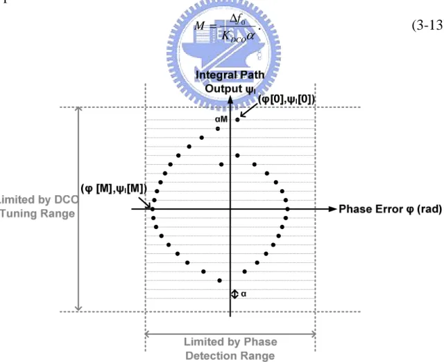
boundary for the trajectory in the phase plane as shown in Fig. 3-11. To derive the frequency capture range of the BBPLL, we will select (φ[0],ΨI[0]) as
starting condition the point immediately before the trajectory moves into the left half-plane. The trajectory starts from this point and it is assumed that the loop has a initial frequency error ∆f0 which implies ΨI[0]=∆f0/KDCO. It should be
noted that when the trajectory lies on the φ axis (ΨI[M]=0) at M-th clock cycle,
the phase error reaches it maximum negative value which is bounded by the phase detection range:
( ) N M π ϕ[ ] 2υ 2 + ≤ . (3-12)
By inspecting the second equation of equation 3-8, the iteration index M can be expressed as α DCO K f M = ∆ 0 . (3-13)
32
In order to calculate the value of φ[M], taking the sum for k=0…i-1 of both members of the first equation of equation 3-8, τ[i] can be written explicitly as [7].
[ ]
[ ]
[ ]
(
)
( )
2 2 ,for 2 2 1 1 0 1 for , 2 1 0 + ≥ + − − − + + + − − + ≤ − − + − − = D i i D i i iD D D iM R D i i i D M iR i τ α τ τ . (3-14)For simplicity, we assume that the initial phase error is negligibly small which leads to τ[0]=0. By noting that M>D+2 for large initial frequency offset, the value of τ[M] can be rewritten as
[ ]
M M M D(
D)
MD− D− +M + + − + − = 1 2 2 2 2 2 β α τ . (3-15)Substituting equation 3-12 and 3-13 into 3-15 and noting that φ=2πfREFNβKTτ
gives
(
)
( ) T REF DCO DCO DCO DCO K N f K f D D D K f D K f K f β α α α α β α υ 2 1 0 0 0 2 0 1 2 2 2 2 1 2 1 ≤ + ∆ − + + + − ∆ + ∆ + ∆ , (3-16) which can be further simplified as(
)
( ) 0 2 2 2 1 2 2 1 2 1 2 2 , 1 2 0 2 0 2 ≤ − + + + − + ∆ − + + ∆ + REF DCO free DCO DCO DCO DCO N K f f D D D f K K D f K β β α α β αβ υ . (3-17)Assume that the condition of equation 3-11 is met. Using a MATLAB script, the relation between loop filter parameters and the allowed maximum initial frequency error ∆f0,max can be solved for a BBPLL having the following
parameters corresponding to our design: fREF=40MHz, N=248, D=0.5, and υ=8.
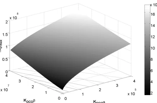
Fig. 3-12 shows the result and it can be seen that the locking range is proportional to the gain KDCOα and KDCOβ as expected.
33
3.2.4
Locking Time of the ADPLL during PT Mode
In the session, the locking time of the BBPLL will be calculated. A similar calculation has been already done in [10] for type II BBPLL where the delay introduced on proportional path is negligibly small compared to the period of reference signal. In our case, the locking time of the BBPLL can be calculated in a similar way. The locking time can be obtained from the number of iterations before the trajectory reaches the origin (BBPLL locked). As shown in Fig. 3-13, consider a trajectory starting from the point (0, M0) and intercepting again the ΨI
axis in (0, M1) at the iteration index i. Since the trajectory can be described by
the equation 3-14, for a given M0, the time index i can be found by solving
equation 3-14 with M=M0/α:
(
)
− − + − − + + + − + + = R R D D D R D M R D M i 1 2 1 2 2 2 1 1 2 1 0 2 0 α α . (3-18)Fig. 3-12 Allowed maximum initial frequency error versus loop parameters KDCOα and KDCOβ for BBPLL. ( fREF=40MHz, N=248, D=0.5, and υ=8.)
34
where the operator x indicates the biggest integer lower or equal to x. In practical cases
(
)
− − + >> − + + R R D D D R D M 2 2 1 2 1 2 1 2 0 α , (3-19)so that i can be simplified to:
− + + ≈ R D M i 2 0 2 1 2 α . (3-20)
The value of M1 is then can be found by noting that M1=M0−iα and from that the
reduction of the radius of the trajectory (∆M) in one half turn around the origin can be obtained:
(
)
α α 2 1 2 1 0 − + = − = ∆ D R M M M . (3-21)As ∆M does not depend on M0, the decrease of the trajectory radius for every
half turn is a constant. Thus, the number of half turns before the trajectory reaches the origin is M0/∆M. By inspecting Fig. 3-13, the total number of
iterations for the BBPLL to be locked is:
Fig. 3-13 Trajectory plot for the computation of the locking time. (Adapted from [7])
35 M M M k M M M M n M M k M M k k tot ∆ = ∆ − + = + =
∑
∑
∆ = ∆ = 2 0 1 0 0 1 0 0 0 2 2 . (3-22)From above expression, it can be seen that for β>>α, the locking speed is proportional to β. To put this equation into practice, the value M0 can be related
to the initial DCO frequency error ∆f0=fOUT-NfREF as
DCO K f M 0 0 ∆ = . (3-23)
In order to evaluate the expression above, consider a BBPLL with the following parameters: ∆f0=6MHz, KDCO=20kHz, α=1, β=32, D=0.5 and
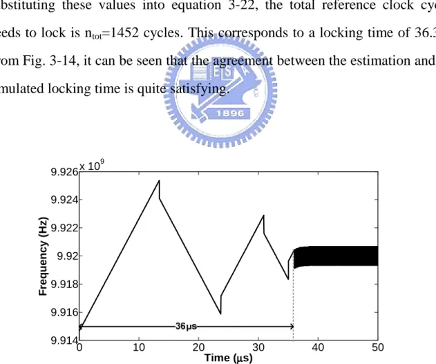
fREF=40MHz. From equation 3-23 and 3-21, M0=300 and ∆M=62. By
substituting these values into equation 3-22, the total reference clock cycles needs to lock is ntot=1452 cycles. This corresponds to a locking time of 36.3µs.
From Fig. 3-14, it can be seen that the agreement between the estimation and the simulated locking time is quite satisfying.
0 10 20 30 40 50 9.914 9.916 9.918 9.92 9.922 9.924 9.926x 10 9 Time (µµµµs) F re q u e n c y ( H z )
Fig. 3-14 Simulation result of DCO output frequency versus time during locking process of BBPLL. (∆f0=6MHz, KDCO=20kHz, α=1, β=32, D=0.5 and
36
3.2.5
Input jitter tolerance of the ADPLL during PT Mode
Since the output of the phase detector during phase tracking can be either +1 or -1, the feedback clock period rate of change is limited to NKTα per clock cycle.This indicates that the BBPLL has an intrinsic limited capability of tracking a reference clock whose period is changing with time. If the rate of the change of the reference frequency is larger than this limit, the loop will go into slew-rate limitation, losing its lock condition. Consider a reference clock fR with a
sinusoidal modulating signal.
( )
t f A(
t)
fR = R0+ modcosωmod , (3-24) where Amod and ωmod are the modulation amplitude and the modulation angular
frequency, respectively. The maximum frequency amplitude that the BBPLL can track can be expressed as [10]
< N K N f K A DCO R β DCO ω α , max mod 0 mod . (3-25)
From equation 3-24, the phase of the FM signal is
( )
t fR t A(
modt)
mod mod 0 sin 2 2 ω ωπ π θ = + . (3-26)Thus, the resulting signal is
( )
(
)
+ = A f t A t t SFM R mod mod mod 0 sin 2 2 sin ω ωπ π . (3-27)Assume that 2πAmod<<ωmod. Equation (14) could be rewritten after some
trigonometric expansion as follows:
( )
t A(
f t)
A A(
t) (
f t)
SFM R mod R0 mod mod 0 sin sin 2 2 2 cos ω π ωπ π − ≈ . (3-28)37
( )
− + ℜ ≈ j f t j t j t FM e A e A Ae t S R0 mod mod mod mod mod mod 2 1 ω ω π ω π ω π . (3-29)From equation 3-29, it is clear that Amod can be mapping to the sidebands with
power 20log(2πAmod/ωmod) dB below the main carrier tone. In this way, we can
define the minimum value of KDCOα and KDCOβ for a given input phase noise.
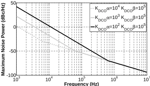
Fig. 3-12 illustrates the limit of the input noise power versus frequency with different KDCOα value.
3.3
Output Noise Performance of the
ADPLL
After the rapid frequency acquisition, the ADPLL will finally reach a steady-state condition in the bang-bang phase tracking mode. The output noise performance in locked state including the spurs, timing jitter and output phase will be investigated. In particular the spur emission will be derived using the
103 104 105 106 107 -100 -50 0 50 Frequency (Hz) M a x im u m N o is e P o w e r (d B c /H z ) K DCOα=10 4 K DCOβ=10 5 K DCOα=10 3 K DCOβ=10 5 K DCOα=10 2 K DCOβ=10 5
Fig. 3-15 Maximum input noise power sufficient to cause slew-limiting as a function frequency and with KDCOα as a parameter.
38
nonlinear model, while the output phase noise performance in the present of internal and external noise source will be analyzed with the help of the linear model.
3.3.1
Output Spur
Due to the presence of the limit cycles or orbit in the dynamics of the BBPLL, the output clock fOUT is frequency modulated by a periodic control signal in
locked state, leading to spurious tone emission.
To gain more insight into the loop dynamics, consider the BBPLL which is free from any internal or external noise source and has the following parameters: fREF=40MHz, α=1, β=128, KDCO=500, D=0.5 and N=248. Fig. 3-16(a) shows the
simulation result of the output frequency versus time in the locked state of the BBPLL with above setting. The result shows that the modulating signal of the carrier is similar to a square wave with some ripples and the modulating rate is equal to 1/4fREF.
Under the assumption of narrow-band frequency modulation, the power level of the spurious tones compared to the carrier can be approximated as [4]:
(dBc) 2 1 log 20 = β spur P , (3-30)
where β is modulation index defined as the ratio of the frequency deviation ∆ω to the frequency of the modulating wave ωm in a frequency modulation system
when using a sinusoidal modulating wave. However, for a symmetric square wave with frequency of ωm as the modulating input, it can be expressed in the
following Fourier series representation:
t n n t g m odd n square ω π sin 1 2 ) ( . 1
∑
∞ = = . (3-31)The modulation index of the nth harmonic for the Fourier series decomposition of a square modulating wave becomes:
![Fig. 2-3 Block diagram of the digital BBPLL architecture proposed in [4].](https://thumb-ap.123doks.com/thumbv2/9libinfo/8011370.160461/24.892.169.764.116.422/fig-block-diagram-digital-bbpll-architecture-proposed.webp)
![Fig. 3-13 Trajectory plot for the computation of the locking time. (Adapted from [7])](https://thumb-ap.123doks.com/thumbv2/9libinfo/8011370.160461/47.892.239.668.130.462/fig-trajectory-plot-computation-locking-time-adapted.webp)