Article
Formation Mechanism of Porous Cu
3
Sn Intermetallic
Compounds by High Current Stressing at High
Temperatures in Low-Bump-Height Solder Joints
Jie-An Lin1, Chung-Kuang Lin1, Chen-Min Liu1, Yi-Sa Huang1, Chih Chen1,*, David T. Chu2 and King-Ning Tu2
Received: 22 November 2015; Accepted: 11 January 2016; Published: 16 January 2016 Academic Editor: Duc Nguyen-Manh
1 Department of Materials Science and Engineering, National Chiao Tung University, Hsinchu 30010, Taiwan;
[email protected] (J.-A.L.); [email protected] (C.-K.L.); [email protected] (C.-M.L.); [email protected] (Y.-S.H.)
2 Department of Materials Science and Engineering, University of California at Los Angeles, Los Angeles,
CA 90095-1595, USA; [email protected] (D.T.C.); [email protected] (K.-N.T.) * Correspondence: [email protected]; Tel.: +886-3-5731814; Fax: +886-3-5724727
Abstract: Electromigration tests of SnAg solder bump samples with 15 µm bump height and Cu under-bump-metallization (UBM) were performed. The test conditions were 1.45 ˆ 104A/cm2at 185˝C and 1.20 ˆ 104A/cm2 at 0˝C. A porous Cu
3Sn intermetallic compound (IMC) structure
was observed to form within the bumps after several hundred hours of current stressing. In direct comparison, annealing alone at 185˝C will take more than 1000 h for porous Cu
3Sn to form, and it
will not form at 170˝C even after 2000 h. Here we propose a mechanism to explain the formation of
this porous structure assisted by electromigration. The results show that the SnAg bump with low bump height will become porous-type Cu3Sn when stressing with high current density and high
temperature. Polarity effects on porous Cu3Sn formation is discussed.
Keywords:intermetallic compounds; porous Cu3Sn; electromigration; side wall reaction
1. Introduction
In the pursuit of higher operation speed and improved performance of microelectronic devices [1], the application of flip chip solder joints has become a key technology for high-density packaging. The solder joints have been used in high power devices, such as central processing unit (CPU) and application processors (AP). The specification of operation temperatures for these devices range from 100 to 110˝C and the required lifetime is usually 10 years. To meet the demand for portable devices,
the input/output pin numbers continue to increase while the size of the solder joints continues to shrink. This inevitably leads to higher current densities and operating temperatures in the joints. Therefore, it raises serious reliability issues such as electromigration and thermomigration [2].
Over the past decades, electromigration behavior and metallurgical reactions of flip chip solder joints have been widely studied [3–9]. The intermetallic compounds (IMC) of Cu3Sn and Cu6Sn5are
commonly formed in solder reactions on Cu under-bump-metallization (UBM). The Cu column-type UBM (a structure with a thicker Cu) was developed to alleviate both the Joule heating and current crowding effects in flip-chip solder joints under normal device operating conditions, having a longer lifetime [10].
Dimensional shrinkage of the solder joints in portable devices may cause new reliability issues. The smaller solder joints tend to transform completely into IMC joints during electromigration tests [11]. Additionally, in low-bump-height solder joints, when they are combined with a thick column-type Cu
Crystals 2016, 6, 12 2 of 10
UBM, the solder reaction on the side wall of the Cu-column becomes one of the new reliability issues of concern. Liang et al. found that in reflow tests, the effect of side wall reaction would lead to the formation of large voids in the solder joints [12].
Panchenko et al. reported a porous Cu3Sn structure in 50 µm pitch Cu/Sn microbump
interconnects during reflow due to the degradation of the Cu6Sn5IMCs layer [13]. The proposed
explanation of the porous Cu3Sn formation is the dissolution of Sn atoms from the Cu6Sn5matrix
owing to the reaction between Cu6Sn5and flux residues. However, the formation mechanism of the
porous Cu3Sn structure has not yet been confirmed.
In this study, we investigated the microstructure evolution of solder joints with Cu column UBM, especially the porous Cu3Sn formation, under current stressing at 1.45 ˆ 104A/cm2at 185˝C and
1.20 ˆ 104A/cm2at 170˝C. We observed the porous Cu
3Sn formation enhanced by current stressing.
2. Experimental Methods
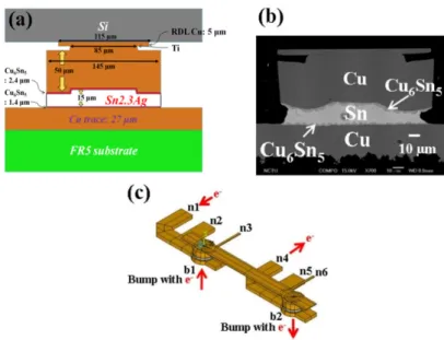
Typical flip-chip solder joints were used in our electromigration tests. Figure1a shows the schematic diagram of a bump with Cu column UBM. On the chip side, 100 nm Ti was sputtered as the adhesion layer. Then a 2 µm Cu layer was sputtered as the seed layer for the subsequent electroplating of a 50 µm Cu UBM column and SnAg solder. The composition of the solder was Sn-2.3Ag. The diameter of UBM and passivation opening is 145 and 85 µm, respectively. The Cu trace on the flame retardant 5 (FR5) substrate is 100 µm wide and 27 µm thick. Pre-solder of Sn-2.3Ag was used on the substrate side. The chips were flipped over to align with the substrates, and they were reflowed at 260˝C for 1 min to form flip-chip solder joints. Figure1b illustrates the cross-sectional SEM images
of a flip-chip bump before the Electromigration EM tests. A scallop-type Cu6Sn5layer was found at
the interface between the Cu metallization and the solder on the chip side, as well as on the substrate side [14].
Crystals 2016, 6, 12 2 of 10
reliability issues of concern. Liang et al. found that in reflow tests, the effect of side wall reaction would lead to the formation of large voids in the solder joints [12].
Panchenko et al. reported a porous Cu3Sn structure in 50 μm pitch Cu/Sn microbump interconnects during reflow due to the degradation of the Cu6Sn5 IMCs layer [13]. The proposed explanation of the porous Cu3Sn formation is the dissolution of Sn atoms from the Cu6Sn5 matrix owing to the reaction between Cu6Sn5 and flux residues. However, the formation mechanism of the porous Cu3Sn structure has not yet been confirmed.
In this study, we investigated the microstructure evolution of solder joints with Cu column UBM, especially the porous Cu3Sn formation, under current stressing at 1.45 × 10⁴ A/cm2 at 185 °C and 1.20 × 10⁴ A/cm2 at 170 °C. We observed the porous Cu3Sn formation enhanced by current stressing. 2. Experimental Methods
Typical flip-chip solder joints were used in our electromigration tests. Figure 1a shows the schematic diagramof a bump with Cu column UBM. On the chip side, 100 nm Ti was sputtered as the adhesion layer. Then a 2 μm Cu layer was sputtered as the seed layer for the subsequent electroplating of a 50 μm Cu UBM column and SnAg solder. The composition of the solder was Sn-2.3Ag. The diameter of UBM and passivation opening is 145 and 85 μm, respectively. The Cu trace on the flame retardant 5 (FR5) substrate is 100 μm wide and 27 μm thick. Pre-solder of Sn-2.3Ag was used on the substrate side. The chips were flipped over to align with the substrates, and they were reflowed at 260 °C for 1 min to form flip-chip solder joints. Figure 1b illustrates the cross-sectional SEM images of a flip-chip bump before the Electromigration EM tests. A scallop-type Cu6Sn5 layer was found at the interface between the Cu metallization and the solder on the chip side, as well as on the substrate side [14].
Figure 1. (a) Schematic of the flip-chip solder joints with Cu column UBM. The redistribution layer
(RDL) on the Si chip is 5-μm thick Cu. (b) Cross-sectional SEM images. (c) Layout for electromigration tests and four-point structure for measuring bump resistance.
Four-point probes were employed to monitor the resistance change during the EM tests of the bump. Figure 1c presents the schematic of the test layout. There are 6 nodes (n1 to n6) in the test layout, and the direction of the electron flow is pointed by the red arrows which shows the two bumps (b1 and b2) were stressed with opposite direction of electron flow. The electrons enter from n1, go upward through b1, then downward through b2, and finally flow out from n6. The resistance change in b1 (b2) can be measured by the voltage drop between n2 and n3 (n5 and n6). In the Figure 1.(a) Schematic of the flip-chip solder joints with Cu column UBM. The redistribution layer (RDL) on the Si chip is 5-µm thick Cu; (b) Cross-sectional SEM images; (c) Layout for electromigration tests and four-point structure for measuring bump resistance.
Four-point probes were employed to monitor the resistance change during the EM tests of the bump. Figure1c presents the schematic of the test layout. There are 6 nodes (n1 to n6) in the test layout, and the direction of the electron flow is pointed by the red arrows which shows the two bumps (b1 and b2) were stressed with opposite direction of electron flow. The electrons enter from n1, go upward through b1, then downward through b2, and finally flow out from n6. The resistance change in b1 (b2) can be measured by the voltage drop between n2 and n3 (n5 and n6). In the microelectronic industry, a
failure is typically defined when the resistance change increases to 20% of its initial value [15]. In our study, the early stage of the tests was defined when the bump resistance increment is smaller than 20% during the EM tests, while the later stage of test was defined when the increment was larger than 20%. The solder joints were stressed with 2.4 A and 2 A at 150˝C. The calculated current densities
were 1.45 ˆ 104A/cm2and 1.20 ˆ 104A/cm2, respectively, based on the UBM opening size. The real temperature in solder joints may be higher than the ambient temperature during current stressing due to Joule heating effect in the stressing condition [6]. Therefore, in our study the temperature coefficient of resistivity (TCR) were employed to measure the real temperature in the joints. The calibrated temperatures were about 185˝C and 170˝C when the test sample was stressed with 2.4 and
2 A, respectively.
Solder joints were cross-sectioned by grinding using abrasive papers #400, #1000, #2000, #2500, and #4000, and then polished by Al2O3of 1 and 0.3 µm. The microstructure and composition were
examined with a JEOL 6500 field-emission scanning electron microscope (SEM) (JEOL Ltd., Tokyo, Japan) and energy dispersive spectroscopy (EDS) (Oxford Instruments, Oxfordshire, UK). The SEM EDS was operated at 15 KeV with a current of 1.0 ˆ 10´5A and a beam size of 1000 nm. Focused ion beam (FIB, FEI Nova 200, FEI Company, Hillsboro, OR, USA) technique was adopted for cross-sectional observation, and transmission electron microscopy (TEM, JEOL-2100F, JEOL Ltd., Tokyo, Japan) and electron probe micro-analyzer (EPMA, JXA-8800M, JEOL Ltd., Tokyo, Japan) were utilized to verify the microstructure results. The operation conditions for the EPMA were at 12 KeV with a current of 1.0 ˆ 10´8A and a beam size of 500 nm.
3. Results and Discussion
3.1. Current-Enhanced IMC Formation
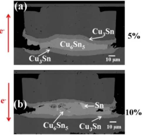
The formation of Cu-Sn IMCs can be significantly enhanced by current stressing. Figure2shows cross-sectional SEM images of a pair of solder joints stressed with 1.45 ˆ 104A/cm2at 185˝C. At the
early stage, the bump resistance increased by 5% (after 283 h in the upward electron flow) and 10% (after 283 h in the downward electron flow) of its initial value, are shown in Figure2a,b, respectively. The current enhanced the dissolution of Cu UBM to react with the solder joint and form a large volume of IMCs. The layer-type Cu6Sn5formed in the middle of the bump and the layer-type Cu3Sn formed
at the interfaces between the Cu and Cu6Sn5. The entire joint almost completely transformed into
IMC joints at the early stage in the EM tests, although there was still some Sn remaining in the bump, as indicated in Figure2b. The results showed that a large volume of IMCs formed at the early stage regardless of the direction of the electron flow.
Crystals 2016, 6, 12 3 of 10
microelectronic industry, a failure is typically defined when the resistance change increases to 20% of its initial value [15]. In our study, the early stage of the tests was defined when the bump resistance increment is smaller than 20% during the EM tests, while the later stage of test was defined when the increment was larger than 20%.
The solder joints were stressed with 2.4 A and 2 A at 150 °C. The calculated current densities were 1.45 × 10⁴ A/cm2 and 1.20 × 10⁴ A/cm2, respectively, based on the UBM opening size. The real temperature in solder joints may be higher than the ambient temperature during current stressing due to Joule heating effect in the stressing condition [6]. Therefore, in our study the temperature coefficient of resistivity (TCR) were employed to measure the real temperature in the joints. The calibrated temperatures were about 185 °C and 170 °C when the test sample was stressed with 2.4 and 2 A, respectively.
Solder joints were cross-sectioned by grinding using abrasive papers #400, #1000, #2000, #2500, and #4000, and then polished by Al2O3 of 1 and 0.3 μm. The microstructure and composition were examined with a JEOL 6500 field-emission scanning electron microscope (SEM) (JEOL Ltd., Tokyo, Japan) and energy dispersive spectroscopy (EDS) (Oxford Instruments, Oxfordshire, UK). The SEM EDS was operated at 15 KeV with a current of 1.0 × 10⁻⁵A and a beam size of 1000 nm. Focused ion beam (FIB, FEI Nova 200, FEI Company, Hillsboro, OR, USA) technique was adopted for cross-sectional observation, and transmission electron microscopy (TEM, JEOL-2100F, JEOL Ltd., Tokyo, Japan) andelectron probe micro-analyzer(EPMA, JXA-8800M, JEOL Ltd., Tokyo, Japan) were utilized to verify the microstructure results. The operation conditions for the EPMA were at 12 KeV with a current of 1.0 × 10⁻⁸ A and a beam size of 500 nm.
3. Results and Discussion
3.1. Current-Enhanced IMC Formation
The formation of Cu-Sn IMCs can be significantly enhanced by current stressing. Figure 2 shows cross-sectional SEM images of a pair of solder joints stressed with 1.45 × 10⁴ A/cm2 at 185 °C. At the early stage, the bump resistance increased by 5% (after 283 h in the upward electron flow) and 10% (after 283 h in the downward electron flow) of its initial value, are shown in Figure 2a,b, respectively. The current enhanced the dissolution of Cu UBM to react with the solder joint and form a large volume of IMCs. The layer-type Cu6Sn5 formed in the middle of the bump and the layer-type Cu3Sn formed at the interfaces between the Cu and Cu6Sn5. The entire joint almost completely transformed into IMC joints at the early stage in the EM tests, although there was still some Sn remaining in the bump, as indicated in Figure 2b. The results showed that a large volume of IMCs formed at the early stage regardless of the direction of the electron flow.
Figure 2. Cross-sectional SEM images of solder bumps with Cu column UBM stressed at 1.45 × 10⁴
A/cm2 at 185 °C with bump resistance increases (a) 5% with upward electron flow and (b) 10% with
downward electron flow.
Figure 2. Cross-sectional SEM images of solder bumps with Cu column UBM stressed at 1.45 ˆ 104A/cm2at 185˝C with bump resistance increases (a) 5% with upward electron flow and
Crystals 2016, 6, 12 4 of 10
3.2. Formation of Porous Cu3Sn
It is interesting that porous Cu3Sn IMCs may form at later stages of electromigration tests.
Figures3and4illustrate the cross-sectional SEM images at different stages in the EM tests with opposite direction of electron flow. Figure3shows the EM test results with upward electron flow. Figure3a–c are the cross-sectional SEM images with bump resistance increase, 8% (after 517 h), 32% (after 217 h), and 85% (after 429 h) of its initial value, respectively. When the bump resistance increased to 8% of its initial value, the layer-type Cu6Sn5in the middle started to transform into porous-type
Cu3Sn, as shown in Figure3a. We note that the porous-type Cu3Sn first formed on the periphery of
the bump. As the change in bump resistance increased to 32%, shown in Figure3b, the layer-type Cu6Sn5IMC had fully transformed into porous-type Cu3Sn IMC. Figure3c shows similar results,
from a different bump, as Figure3b which means the Cu6Sn5IMC had also totally transformed into
porous-type Cu3Sn IMCs in the later stage of the EM tests.
Crystals 2016, 6, 12 4 of 10
3.2. Formation of Porous Cu3Sn
It is interesting that porous Cu3Sn IMCs may form at later stages of electromigration tests.
Figures 3 and 4 illustrate the cross-sectional SEM images at different stages in the EM tests with opposite direction of electron flow. Figure 3 shows the EM test results with upward electron flow. Figure 3a–c are the cross-sectional SEM images with bump resistance increase, 8% (after 517 h), 32% (after 217 h), and 85% (after 429 h) of its initial value, respectively. When the bump resistance increased to 8% of its initial value, the layer-type Cu6Sn5 in the middle started to transform into
porous-type Cu3Sn, as shown in Figure 3a. We note that the porous-type Cu3Sn first formed on the
periphery of the bump. As the change in bump resistance increased to 32%, shown in Figure 3b, the layer-type Cu6Sn5 IMC had fully transformed into porous-type Cu3Sn IMC. Figure 3c shows similar
results, from a different bump, as Figure 3b which means the Cu6Sn5 IMC had also totally transformed
into porous-type Cu3Sn IMCs in the later stage of the EM tests.
Figure 3. Cross-sectional SEM images of solder bumps with Cu column UBM stressed at 1.45 × 10⁴
A/cm2 with upward electron flow at 185 °C with bump resistance increases (a) 8%, (b) 32%, and (c)
85% of its initial value.
Similarly, Figure 4 shows the EM tests results with downward electron flow, where Figure 4a–c illustrate the cross-sectional SEM images with the bump resistance increase 15% (after 517 h), 20% (after 217 h), and 100% (after 429 h) of its initial value, respectively. The results are similar to those in Figure 3. As the bump resistance increased, the layer-type Cu6Sn5 in the middle started to
transform into porous-type Cu3Sn.
In order to rule out the possibility that the porous structure was generated in the polishing process or by other external forces, FIB were utilized to provide a deeper cross-section in a selected solder joint, stressed at 1.45 × 10⁴ A/cm2 for 429 h as illustrated in Figure 5. The downward direction
of the electron flow was labeled in the figure. This second cross-section view indicated that the porous structure not only formed on the polished surface but in the entire bump.
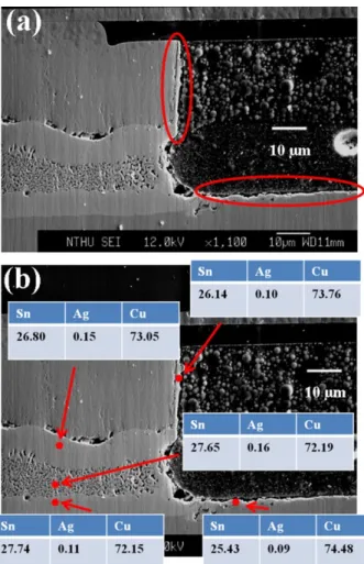
In the bumps with porous Cu3Sn, we observed that the effect of side wall reaction is very serious.
Park et al. reported that a high stressing current may lead to a serious side wall reaction effect [16]. Figure 6a shows the side wall of a bump. The bump has had porous-type Cu3Sn IMCs formation. We
can clearly observe that there are IMCs formation on the side wall, indicated by the ellipses. Since the thickness of the IMCs formed on the side wall is only about 3 μm, it is hard to verify the composition with EDS. Hence, EPMA was used instead. Figure 6b illustrates the results that all the IMCs formed on the side wall are Cu3Sn. The compositions of the layer-type and porous-type structures were also
confirmed with EPMA to be Cu3Sn, identical with the results measured with EDS. Therefore, the whole
joint has transformed completely into Cu3Sn with two different morphologies.
Figure 3. Cross-sectional SEM images of solder bumps with Cu column UBM stressed at 1.45 ˆ 104A/cm2 with upward electron flow at 185 ˝C with bump resistance increases (a) 8%,
(b) 32%, and (c) 85% of its initial value.
Similarly, Figure4shows the EM tests results with downward electron flow, where Figure4a–c illustrate the cross-sectional SEM images with the bump resistance increase 15% (after 517 h), 20% (after 217 h), and 100% (after 429 h) of its initial value, respectively. The results are similar to those in Figure3. As the bump resistance increased, the layer-type Cu6Sn5in the middle started to transform
into porous-type Cu3Sn.
In order to rule out the possibility that the porous structure was generated in the polishing process or by other external forces, FIB were utilized to provide a deeper cross-section in a selected solder joint, stressed at 1.45 ˆ 104A/cm2for 429 h as illustrated in Figure5. The downward direction of the electron flow was labeled in the figure. This second cross-section view indicated that the porous structure not only formed on the polished surface but in the entire bump.
In the bumps with porous Cu3Sn, we observed that the effect of side wall reaction is very serious.
Park et al. reported that a high stressing current may lead to a serious side wall reaction effect [16]. Figure6a shows the side wall of a bump. The bump has had porous-type Cu3Sn IMCs formation. We
can clearly observe that there are IMCs formation on the side wall, indicated by the ellipses. Since the thickness of the IMCs formed on the side wall is only about 3 µm, it is hard to verify the composition with EDS. Hence, EPMA was used instead. Figure6b illustrates the results that all the IMCs formed on the side wall are Cu3Sn. The compositions of the layer-type and porous-type structures were also
confirmed with EPMA to be Cu3Sn, identical with the results measured with EDS. Therefore, the whole
Figure7shows the cross-sectional TEM image and the electron diffraction patterns of point “a” in a porous Cu3Sn. In the diffraction pattern, the spots correspond to the principle reflections of a
basic hexagonal lattice. The zone axes are indexed with [0112]. The results show that the porous-type structure is hexagonal Cu3Sn.
Figure 7 shows the cross-sectional TEM image and the electron diffraction patterns of point “a” in a porous Cu3Sn. In the diffraction pattern, the spots correspond to the principle reflections of a
basic hexagonal lattice. The zone axes are indexed with [01 1 2]. The results show that the porous-type structure is hexagonal Cu3Sn.
Figure 4. Cross-sectional SEM images of solder bumps with Cu column UBM stressed at 1.45 × 10⁴ A/cm2 with downward electron flow at 185 °C with bump resistance increases (a) 15%,
(b) 20%, and (c) 100% of its initial value. Cross-sectional SEM images of solder bumps with Cu column UBM stressed at 1.45 × 10⁴ A/cm2 with downward electron flow at 185 °C with bump resistance
increases (a) 15%, (b) 20%, and (c) 100% of its initial value.
Figure 5. Cross-sectional FIB image of Cu3Sn IMC structures.
To determine the conditions under which porous Cu3Sn could form, we stressed the sample at
a lower current density and, hence, a lower temperature. Figure 8 shows cross-sectional SEM images of a pair of solder joints stressed with 1.2 × 10⁴ A/cm2 at 170 °C. The bump resistance increases 140%
(after 5094 h) and 530% (after 5094 h) of its initial value as indicated in Figure 8a and 8b, respectively. It can be seen that only layer-type Cu3Sn and layer-type Cu6Sn5 have formed, with no evidence of
porous Cu3Sn even in the case of Figure 8b. The results demonstrate that the solder joints do not
transform into porous structures at an insufficient current density and temperature.
Figure 4. Cross-sectional SEM images of solder bumps with Cu column UBM stressed at 1.45 ˆ 104A/cm2with downward electron flow at 185˝C with bump resistance increases (a) 15%,
(b) 20%, and (c) 100% of its initial value. Cross-sectional SEM images of solder bumps with Cu column UBM stressed at 1.45 ˆ 104A/cm2with downward electron flow at 185˝C with bump resistance
increases (a) 15%, (b) 20%, and (c) 100% of its initial value.
Figure 7 shows the cross-sectional TEM image and the electron diffraction patterns of point “a” in a porous Cu3Sn. In the diffraction pattern, the spots correspond to the principle reflections of a
basic hexagonal lattice. The zone axes are indexed with [01 1 2]. The results show that the porous-type structure is hexagonal Cu3Sn.
Figure 4. Cross-sectional SEM images of solder bumps with Cu column UBM stressed at 1.45 × 10⁴ A/cm2 with downward electron flow at 185 °C with bump resistance increases (a) 15%,
(b) 20%, and (c) 100% of its initial value. Cross-sectional SEM images of solder bumps with Cu column UBM stressed at 1.45 × 10⁴ A/cm2 with downward electron flow at 185 °C with bump resistance
increases (a) 15%, (b) 20%, and (c) 100% of its initial value.
Figure 5. Cross-sectional FIB image of Cu3Sn IMC structures.
To determine the conditions under which porous Cu3Sn could form, we stressed the sample at
a lower current density and, hence, a lower temperature. Figure 8 shows cross-sectional SEM images of a pair of solder joints stressed with 1.2 × 10⁴ A/cm2 at 170 °C. The bump resistance increases 140%
(after 5094 h) and 530% (after 5094 h) of its initial value as indicated in Figure 8a and 8b, respectively. It can be seen that only layer-type Cu3Sn and layer-type Cu6Sn5 have formed, with no evidence of
porous Cu3Sn even in the case of Figure 8b. The results demonstrate that the solder joints do not
transform into porous structures at an insufficient current density and temperature. Figure 5.Cross-sectional FIB image of Cu3Sn IMC structures.
To determine the conditions under which porous Cu3Sn could form, we stressed the sample at a
lower current density and, hence, a lower temperature. Figure8shows cross-sectional SEM images of a pair of solder joints stressed with 1.2 ˆ 104A/cm2at 170˝C. The bump resistance increases 140%
(after 5094 h) and 530% (after 5094 h) of its initial value as indicated in Figure8a,b, respectively. It can be seen that only layer-type Cu3Sn and layer-type Cu6Sn5have formed, with no evidence of porous
Cu3Sn even in the case of Figure8b. The results demonstrate that the solder joints do not transform
Crystals 2016, 6, 12 6 of 10
Crystals 2016, 6, 12 6 of 10
Figure 6. Cross-sectional SEM images of (a) IMCs formed on the side wall and (b) EPMA analysis. The composition data were shown in atomic percent.
Figure 7. (a) Cross-sectional TEM image of porous-type structure and (b) diffraction patterns of point A in (a). To further examine the temperature effect on the of porous Cu3Sn formation, another set of
bumps were aged at 185 °C in the oven without current stressing. In the case of 1000-h aging (Figure Figure 6.Cross-sectional SEM images of (a) IMCs formed on the side wall and (b) EPMA analysis. The composition data were shown in atomic percent.
Crystals 2016, 6, 12 6 of 10
Figure 6. Cross-sectional SEM images of (a) IMCs formed on the side wall and (b) EPMA analysis. The composition data were shown in atomic percent.
Figure 7. (a) Cross-sectional TEM image of porous-type structure and (b) diffraction patterns of point A in (a). To further examine the temperature effect on the of porous Cu3Sn formation, another set of
bumps were aged at 185 °C in the oven without current stressing. In the case of 1000-h aging (Figure Figure 7.(a) Cross-sectional TEM image of porous-type structure and (b) diffraction patterns of point A in (a).
To further examine the temperature effect on the of porous Cu3Sn formation, another set of bumps
were aged at 185˝C in the oven without current stressing. In the case of 1000-h aging (Figure9a), the
joints have fully transformed into IMC joints. Layer-type Cu6Sn5has formed in the middle of the bump
and layer-type Cu3Sn has formed between Cu and Cu6Sn5. In the case of 2000 h aging (Figure9b), the
layer-type Cu6Sn5in the middle has completely transformed into porous Cu3Sn. The results show that
porous Cu3Sn could form without current stressing at a sufficiently high temperature, which gives an
independent confirmation of temperature’s critical role in the formation of porous Cu3Sn.
Crystals 2016, 6, 12 7 of 10
9a), the joints have fully transformed into IMC joints. Layer-type Cu6Sn5 has formed in the middle of
the bump and layer-type Cu3Sn has formed between Cu and Cu6Sn5. In the case of 2000 h aging
(Figure 9b), the layer-type Cu6Sn5 in the middle has completely transformed into porous Cu3Sn. The
results show that porous Cu3Sn could form without current stressing at a sufficiently high
temperature, which gives an independent confirmation of temperature’s critical role in the formation of porous Cu3Sn.
Figure 8. Cross-sectional SEM images of solder bumps with Cu column UBM stressed at 1.20 × 10⁴ A/cm2 at 170 °C with bump resistance increases (a) 140% with upward electron flow and
(b) 530% with downward electron flow.
Figure 9. Cross-sectional SEM images of solder bumps with Cu column UBM aging at 185 °C for (a) 1000 h and (b) 2000 h.
So far, we have observed that the porous-type Cu3Sn IMCs can form during high current
stressing at high temperatures and the effect of side wall wetting is obvious. To explain its formation mechanism, a further discussion is presented in the next section.
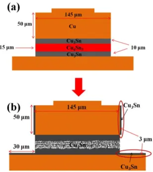
3.3. Formation Mechanism of Porous Cu3Sn IMCs
On the formation mechanism of porous Cu3Sn, first, the temperature must be high enough.
Second, the solder height must be low enough so that the Cu supply is enough for the whole joint to transform into IMC. This is because when there are unreacted solders in the joints, the major IMC is Cu6Sn5 after the metallurgical reactions, as illustrated in Figure 1b. Only a thin layer of Cu3Sn
presented between the Cu metallization layer and the Cu6Sn5 IMCs. The transformation process is
schematically illustrated in Figure 10. In the early stage of the EM tests, layer-type Cu6Sn5 and Cu3Sn
formed first, as shown in Figure 10a. As the bump resistance increased, the layer-type Cu6Sn5 started
to transform into porous-type Cu3Sn, as illustrated in Figure 10b. The IMCs formed on the side walls
due to the effect of side wall reaction are also shown in Figure 10b, labeled by the ellipses.
According to the experimental results, we have developed the following mechanism to explain the formation of the porous-type Cu3Sn. Previously, the Kirkendall void formation mechanism in
Cu3Sn was proposed [17]. When the layer-type Cu6Sn5 decomposes into Cu3Sn, it will release 3 Sn atoms: Figure 8. Cross-sectional SEM images of solder bumps with Cu column UBM stressed at 1.20 ˆ 104A/cm2 at 170 ˝C with bump resistance increases (a) 140% with upward electron flow
and (b) 530% with downward electron flow.
Crystals 2016, 6, 12 7 of 10
9a), the joints have fully transformed into IMC joints. Layer-type Cu6Sn5 has formed in the middle of
the bump and layer-type Cu3Sn has formed between Cu and Cu6Sn5. In the case of 2000 h aging
(Figure 9b), the layer-type Cu6Sn5 in the middle has completely transformed into porous Cu3Sn. The
results show that porous Cu3Sn could form without current stressing at a sufficiently high
temperature, which gives an independent confirmation of temperature’s critical role in the formation of porous Cu3Sn.
Figure 8. Cross-sectional SEM images of solder bumps with Cu column UBM stressed at 1.20 × 10⁴ A/cm2 at 170 °C with bump resistance increases (a) 140% with upward electron flow and
(b) 530% with downward electron flow.
Figure 9. Cross-sectional SEM images of solder bumps with Cu column UBM aging at 185 °C for (a) 1000 h and (b) 2000 h.
So far, we have observed that the porous-type Cu3Sn IMCs can form during high current
stressing at high temperatures and the effect of side wall wetting is obvious. To explain its formation mechanism, a further discussion is presented in the next section.
3.3. Formation Mechanism of Porous Cu3Sn IMCs
On the formation mechanism of porous Cu3Sn, first, the temperature must be high enough.
Second, the solder height must be low enough so that the Cu supply is enough for the whole joint to transform into IMC. This is because when there are unreacted solders in the joints, the major IMC is Cu6Sn5 after the metallurgical reactions, as illustrated in Figure 1b. Only a thin layer of Cu3Sn
presented between the Cu metallization layer and the Cu6Sn5 IMCs. The transformation process is
schematically illustrated in Figure 10. In the early stage of the EM tests, layer-type Cu6Sn5 and Cu3Sn
formed first, as shown in Figure 10a. As the bump resistance increased, the layer-type Cu6Sn5 started
to transform into porous-type Cu3Sn, as illustrated in Figure 10b. The IMCs formed on the side walls
due to the effect of side wall reaction are also shown in Figure 10b, labeled by the ellipses.
According to the experimental results, we have developed the following mechanism to explain the formation of the porous-type Cu3Sn. Previously, the Kirkendall void formation mechanism in
Cu3Sn was proposed [17]. When the layer-type Cu6Sn5 decomposes into Cu3Sn, it will release 3 Sn atoms: Figure 9. Cross-sectional SEM images of solder bumps with Cu column UBM aging at 185˝C for
(a) 1000 h and (b) 2000 h.
So far, we have observed that the porous-type Cu3Sn IMCs can form during high current stressing
at high temperatures and the effect of side wall wetting is obvious. To explain its formation mechanism, a further discussion is presented in the next section.
3.3. Formation Mechanism of Porous Cu3Sn IMCs
On the formation mechanism of porous Cu3Sn, first, the temperature must be high enough.
Second, the solder height must be low enough so that the Cu supply is enough for the whole joint to transform into IMC. This is because when there are unreacted solders in the joints, the major IMC is Cu6Sn5after the metallurgical reactions, as illustrated in Figure1b. Only a thin layer of Cu3Sn
presented between the Cu metallization layer and the Cu6Sn5IMCs. The transformation process is
schematically illustrated in Figure10. In the early stage of the EM tests, layer-type Cu6Sn5and Cu3Sn
formed first, as shown in Figure10a. As the bump resistance increased, the layer-type Cu6Sn5started
to transform into porous-type Cu3Sn, as illustrated in Figure10b. The IMCs formed on the side walls
Crystals 2016, 6, 12 8 of 10
According to the experimental results, we have developed the following mechanism to explain the formation of the porous-type Cu3Sn. Previously, the Kirkendall void formation mechanism in Cu3Sn
was proposed [17]. When the layer-type Cu6Sn5decomposes into Cu3Sn, it will release 3 Sn atoms:
Cu6Sn5Ñ2Cu3Sn ` 3Sn (1)
The Sn atoms will then attract nine Cu atoms to form three more Cu3Sn.
3Sn ` 9Cu Ñ 3Cu3Sn (2)
Crystals 2016, 6, 12 8 of 10
Cu6Sn5 → 2Cu3Sn + 3Sn (1)
The Sn atoms will then attract nine Cu atoms to form three more Cu3Sn.
3Sn + 9Cu → 3Cu3Sn (2)
Figure 10. Schematic diagrams of transformation process at (a) early stage and (b) final stage in the electromigration tests.
The vacancies which enable the diffusion of the Cu atoms tend to form Kirkendall voids in Cu3Sn. It implies that the growth of layer-type Cu3Sn IMCs is at the expense of layer-type Cu6Sn5
IMCs. However, in our experimental results, it can be observed that as the layer-type Cu3Sn IMCs
grew to certain thickness, the layer-type Cu6Sn5 would not transform into the layer-type but
porous-type Cu3Sn. Hsiao et al. found that Cu-Sn IMCs can become a diffusion barrier for the
Cu/solder reaction [18]. We assume that the layer-type Cu3Sn served as a diffusion barrier and
inhibited the Sn atoms released from the decomposition of Cu6Sn5 to react with Cu. Since the bumps
were stressed with high current density at high temperature, the released Sn diffused to the side wall to form Cu3Sn due to the effect of the side wall reaction. The place originally occupied by Sn became
empty and led to the porous-type structure.
3.4. Polarity Effect
We have observed the polarity effect in the final stage of the EM tests; namely, more porous structures formed on the anode side than on the cathode side. By the mechanism theorized above, the phenomenon was caused by an abundant Cu supply on the cathode side than on the anode side. Hence, there was more Cu3Sn formation on the cathode side. However, Cu atoms were less likely to
diffuse to the anode side to react with the released Sn. As a result, the porous structure was more obvious on the anode side. The polarity effect is, thus, a consequence of the proposed mechanism.
3.5. Theoretical Calculation of Pore Volume
This mechanism can be further verified by volume calculations. One mole of Cu6Sn5 decomposes
into two moles of Cu3Sn plus three moles of Sn. Approximately, one mole of Cu6Sn5 has a volume of
117.7 cm3, two moles of Cu3Sn has a volume of 69.5 cm3, and three moles of Sn has a volume of
48.4 cm3. In our observation, the volume before and after the Cu6Sn5 to Cu3Sn conversion was nearly
unchanged (117.7 to 117.9 cm3). Calculations also indicate that the volume change in phase
transformation is negligible. On the other hand, the diffusion of Sn to the side walls would leave the Figure 10.Schematic diagrams of transformation process at (a) early stage and (b) final stage in the electromigration tests.
The vacancies which enable the diffusion of the Cu atoms tend to form Kirkendall voids in Cu3Sn.
It implies that the growth of layer-type Cu3Sn IMCs is at the expense of layer-type Cu6Sn5IMCs.
However, in our experimental results, it can be observed that as the layer-type Cu3Sn IMCs grew to
certain thickness, the layer-type Cu6Sn5would not transform into the layer-type but porous-type Cu3Sn.
Hsiao et al. found that Cu-Sn IMCs can become a diffusion barrier for the Cu/solder reaction [18]. We assume that the layer-type Cu3Sn served as a diffusion barrier and inhibited the Sn atoms released from
the decomposition of Cu6Sn5to react with Cu. Since the bumps were stressed with high current density
at high temperature, the released Sn diffused to the side wall to form Cu3Sn due to the effect of the side
wall reaction. The place originally occupied by Sn became empty and led to the porous-type structure. 3.4. Polarity Effect
We have observed the polarity effect in the final stage of the EM tests; namely, more porous structures formed on the anode side than on the cathode side. By the mechanism theorized above, the phenomenon was caused by an abundant Cu supply on the cathode side than on the anode side. Hence, there was more Cu3Sn formation on the cathode side. However, Cu atoms were less likely
to diffuse to the anode side to react with the released Sn. As a result, the porous structure was more obvious on the anode side. The polarity effect is, thus, a consequence of the proposed mechanism.
3.5. Theoretical Calculation of Pore Volume
This mechanism can be further verified by volume calculations. One mole of Cu6Sn5decomposes
into two moles of Cu3Sn plus three moles of Sn. Approximately, one mole of Cu6Sn5has a volume
of 117.7 cm3, two moles of Cu3Sn has a volume of 69.5 cm3, and three moles of Sn has a volume
of 48.4 cm3. In our observation, the volume before and after the Cu6Sn5to Cu3Sn conversion was
nearly unchanged (117.7 to 117.9 cm3). Calculations also indicate that the volume change in phase
transformation is negligible. On the other hand, the diffusion of Sn to the side walls would leave the pores behind. Assuming that the pore volume equals that of the released Sn, we have calculated the volume occupied by pores to be 41.2% (48.4/117.9) of the porous Cu3Sn volume, when all the released
Sn atoms diffuse to the side walls of the UBMs. As a verification, we have used software to calculate the volume percentage of the pores in the actual bumps. Six bumps were input into the software to ensure accuracy. The average volume percentage of the pores was found to be 38.2%, a number close to the theoretical 41.2%. The volume of pores (or the volume of the released Sn) in the bumps is approximately 63,879 µm3. We assume that all of released Sn atoms have diffused to the side walls to
form Cu3Sn. This implies that 63,879 µm3of Sn would form 137,978 µm3of Cu3Sn on the side walls.
This is again close to the calculated value of 157,932 µm3for the volume of Cu3Sn formed on the side
walls in the actual bumps.
The above experimental results and calculation both indicate Sn diffusion to side walls of Cu UBM may be a possible mechanism for the formation of the porous Cu3Sn. The porous Cu3Sn will be a
reliability issue for solder joints with Cu UBM. Yet, no solutions have been proposed so far to prevent it from happening. More studies need to be performed to solve this problem.
4. Conclusions
We have carried out a systematic study on an important reliability issue related to high-density packaging of microelectronic devices. In this study, SnAg solder bump samples with Cu UBM were stressed at current densities of 1.45 ˆ 104A/cm2and 1.20 ˆ 104A/cm2and operating temperatures of approximately 185˝C and 170˝C, respectively. A porous Cu
3Sn structure, unseen in traditional
flip-chip solder joints, was observed in the process. Cu3Sn IMCs were also observed on the side walls
of Cu column UBM due to side wall reactions. We have proposed a theory to explain the formation mechanism of the observed porous Cu3Sn and side-wall Cu3Sn. In the reaction: Cu6Sn5Ñ2Cu3Sn +
3Sn, one Cu6Sn5molecule converted into three Cu3Sn molecules and three Sn atoms were released.
The released Sn left pores behind to form the porous Cu3Sn. This is because when the early formed
layer-type Cu3Sn becomes a barrier to Cu diffusion, the released Sn atoms, taking an alternative path,
diffuse to the side walls to form the Cu3Sn IMCs by side wall reaction. Results of volume calculations
were consistent with the proposed processes and consequently provided further evidence of this mechanism. In the past, the layer-type Cu3Sn is regarded as the terminal phase for the solid-state
Cu-Sn reactions; however, our results conclude that the SnAg bump with low bump height would lead to porous-type Cu3Sn formation when it is stressed with high current densities and high temperatures.
Acknowledgments:Financial support from the Ministry of Science and Technology, Taiwan, under the contract of 101-2628-E-009-017-MY3 is acknowledged.
Author Contributions:J.-A.L. contributed to electromigration tests and co-wrote the paper. C.-K.L. contributed electromigration tests and SEM analysis. C.-M.L contributed to TEM analysis. Y.-S.H. contributed to TEM sample preparation. D.T.C contributes to void analysis and discussion. C.C. and K.-N.T led the study and co-wrote the paper.
Conflicts of Interest:The authors declare no conflict of interest. References
1. Tu, K.N. Recent advances on electromigration in very-large-scale-integration of interconnects. J. Appl. Phys. 2003, 94, 5451–5473. [CrossRef]
Crystals 2016, 6, 12 10 of 10
2. Chen, C.; Tong, H.M.; Tu, K.N. Electromigration and Thermomigration in Pb-Free Flip-Chip Solder Joints. Rev. Mater. Sci. 2010, 40, 531–555. [CrossRef]
3. Chen, C.; Liang, S.W. Electromigration issues in lead-free solder joints. J. Mater. Sci. Mater. Electron. 2007, 18, 259–268. [CrossRef]
4. Chu, M.H.; Liang, S.W.; Chen, C.; Huang, A.T. Electromigration Failure Mechanism in Sn-Cu Solder Alloys with OSP Cu Surface Finish. J. Electron. Mater. 2012, 41, 2502–2507. [CrossRef]
5. Zeng, K.; Tu, K.N. Six cases of reliability study of Pb-free solder joints in electronic packaging technology. Mater. Sci. Eng. R Rep. 2002, 38, 55–105. [CrossRef]
6. Chiu, S.H.; Chen, C. Investigation of void nucleation and propagation during electromigration of flip-chip solder joints using x-ray microscopy. Appl. Phys. Lett. 2006, 89. [CrossRef]
7. Liu, C.Y.; Chen, C.; Liao, C.N.; Tu, K.N. Microstructure-electromigration correlation in a thin stripe of eutectic SnPb solder stressed between Cu electrodes. Appl. Phys. Lett. 1999, 75, 58–60. [CrossRef]
8. Liang, S.W.; Chang, Y.W.; Shao, T.L.; Chen, C.; Tu, K.N. Effect of three-dimensional current and temperature distributions on void formation and propagation in flip-chip solder joints during electromigration. Appl. Phys. Lett. 2006, 89, 022117. [CrossRef]
9. Liang, S.W.; Chiu, S.H.; Chen, C. Effect of Al-trace degradation on Joule heating during electromigration in flip-chip solder joints. Appl. Phys. Lett. 2007, 90, 082103. [CrossRef]
10. Liang, Y.C.; Tsao, W.A.; Chen, C.; Yao, D.; Huang, A.T.; Lai, Y. Influence of Cu column under-bump-metallizations on current crowding and Joule heating effects of electromigration in flip-chip solder joints. J. Appl. Phys. 2012, 111, 043705. [CrossRef]
11. Xu, L.; Han, J.; Liang, J.J.; Tu, K.N.; Lai, Y. Electromigration induced high fraction of compound formation in SnAgCu flip chip solder joints with copper column. Appl. Phys. Lett. 2008, 92, 262104. [CrossRef]
12. Liang, Y.C.; Chen, C.; Tu, K.N. Side Wall Wetting Induced Void Formation due to Small Solder Volume in Microbumps of Ni/SnAg/Ni upon Reflow. ECS Solid State Lett. 2012, 1, 60–62. [CrossRef]
13. Panchenko, I.; Croes, K.; Wolf, I.D.; Messemaeker, J.D.; Beyne, E.; Wolter, K. Degradation of Cu6Sn5
intermetallic compound by pore formation in solid-liquid interdiffusion Cu/Sn microbump interconnects. Microelectron. Eng. 2014, 117, 26–34. [CrossRef]
14. Tu, K.N. Solder Joint Technology; Springer: New York, NY, USA, 2007.
15. Joint Electron Device Engineering Council (JEDEC). Guideline for Characterizing Solder Bump Electromigration Under Constant Current and Temperature Stress; JEDEC Standard JEP154; JEDEC: Arlington, VA, USA, 2008. 16. Park, Y.; Kim, S.; Park, J.; Kim, J.; Son, H.; Han, K.; Oh, J.; Kim, N.; Yoo, S. Current Density Effects on the
Electrical Reliability of Ultra Fine-Pitch Micro-Bump for TSV Integration. In Proceedings of the 2013 IEEE 63rd Electronic Components and Technology Conference, Las Vegas, NV, USA, 28–31 May 2013.
17. Zeng, K.; Stierman, R.; Chiu, T.; Edwards, D.; Ano, K.; Tu, K.N. Kirkendall void formation in eutectic SnPb solder joints on bare Cu and its effect on joint reliability. J. Appl. Phys. 2005, 97, 024508. [CrossRef]
18. Hsiao, H.Y.; Hu, C.; Guo, M.; Chen, C.; Tu, K.N. Inhibiting the consumption of Cu during multiple reflows of Pb-free solder on Cu. Scr. Mater. 2011, 65, 907–910. [CrossRef]
© 2016 by the authors; licensee MDPI, Basel, Switzerland. This article is an open access article distributed under the terms and conditions of the Creative Commons by Attribution (CC-BY) license (http://creativecommons.org/licenses/by/4.0/).