國 立 交 通 大 學
電子工程學系 電子研究所碩士班
碩 士 論 文
射頻前端接收器設計
RF Front-end Receiver Design
研 究 生 : 蔡 順 意
指導教授 : 胡 樹 一 博 士
射頻前端接收器設計
RF Front-end Receiver Design
研 究 生 : 蔡 順 意 Student: Shun-I Tsai
指導教授 : 胡 樹 一 博 士 Advisor: Dr. Robert Hu
國 立 交 通 大 學
電 子 工 程 學 系 電 子 研 究 所 碩 士 班
碩 士 論 文
A Thesis
Submitted to Department of Electronics Engineering & Institute of Electronics College of Electrical and Computer Engineering
National Chiao Tung University in Partial Fulfillment of the Requirements
for the Degree of Master In
Electronics Engineering 2007
HsinChu, Taiwan, Republic of China
國 立 交 通 大 學
博碩士論文全文電子檔著作權授權書
(提供授權人裝訂於紙本論文書名頁之次頁用)
本授權書所授權之學位論文,為本人於國立交通大學 電子工程學 系所 _乙_組, 九十六 學年度第_一_學期取得碩士學位之論文。 論文題目:RF Front-end Receiver Design
指導教授:胡 樹 一 博 士 ■ 同意 □不同意 本人茲將本著作,以非專屬、無償授權國立交通大學與台灣聯合大學系統 圖書館:基於推動讀者間「資源共享、互惠合作」之理念,與回饋社會與 學術研究之目的,國立交通大學及台灣聯合大學系統圖書館得不限地域、 時間與次數,以紙本、光碟或數位化等各種方法收錄、重製與利用;於著 作權法合理使用範圍內,讀者得進行線上檢索、閱覽、下載或列印。 論文全文上載網路公開之範圍及時間: 本校及台灣聯合大學系統區域網路 ■ 中華民國一百年一月一日公開 校外網際網路 ■ 中華民國一百年一月一日公開 授 權 人:蔡 順 意 親筆簽名:______________________ 中華民國 九十六 年 十一 月 二十九 日
射 頻 前 端 接 收 器 設 計
研究生 : 蔡順意 指導教授 : 胡樹一 博 士
國立交通大學 電子工程學系 電子研究所碩士班摘要
本篇論文提出一個 4GHz 到 20GHz 的低雜訊寬
頻放大器,和一種新穎被動式混波器。低雜訊寬頻放
大器是運用 4 顆電晶體,接成共源極的架構;利用輸
入閘極電感和並聯回授電容,來完成輸入阻抗匹配。
整體放大器在工作頻率範圍,功率增益可達 22 dB,
輸入反射係數低於 -10dB。最後在臺灣基體電路公司
下線,使用 0.18 微米互補性氧化金屬半導體製程。
被動式混波器是一種全新的架構,從未被發表在國際
期刊。這個架構沒有直流功率消耗,沒有 1 dB 功率
抑制點;在沒有慮波器的情形下,輸出中頻的載波和
射頻訊號可被有效消除。
RF Front-end Receiver Design
Student: Tsai Shun-I Advisor: Dr. Robert Hu
Department of Electronic Engineering & Institute of Electronics
National Chiao Tung University
Abstract
This thesis presents a 4GHz to 20GHz low noise
amplifier, and a novel architecture of mixer. Low noise
amplifier utilizes four MOS transistors which are designed
as common-mode source architecture, and apply gate
inductor and parallel-feedback capacitor to achieve
wide-band input impedance matching. Power gain can be up
to 22dB and input reflection coefficient can be lower than
-10dB on intended frequency range, and is fabricated in
TSMC 0.18μm CMOS technology. The passive mixer is a
novel architecture, and is never published on worldwide
international papers. This architecture doesn’t consume any
DC power and no 1-dB compression issue. Besides, at IF
output terminal, LO and RF signals can be effectively
eliminated without any filters.
致謝
感謝胡樹一老師三年來的教導,無論在研究上或其他
方面,老師真的很感謝您。謝謝 319 實驗室博士班學
長 Fadi,他在 ADS 上的指導;謝謝本實驗室全體同學
適時的幫助。最後要感謝父母背後的支持,讓我全心
全意完成學業,謝謝。
Table of Contents
摘要... i Abstract... ii 致謝... iii Table of Contents ... iv Figure Captions... vi Chapter 1 Introduction...1 1.1 Motivation...11.2 A Brief Wireless History...2
1.3 Introduce to The Standards on Wireless Communication System ...4
1.3.1 Wi-Fi ...4
1.3.1 BlueTooth...6
Chapter 2 The Principal Concepts of Designing Low Noise Amplifier and Mixer ...7
2.1 Introduction Noise Sources...7
2.1.1 Shot Noise...8
2.1.2 Thermal Noise...9
2.1.3 Flicker Noise... 11
2.1.4 Burst Noise...12
2.1.5 Avalanche Noise ...14
2.2 The Principal Concepts of Low Noise Amplifier ...16
2.2.1 Classical Noise Matching Technique...17
2.2.2 Simultaneous Noise and Input Matching Technique ...19
2.2.3 Power-Constrained Simultaneous Noise and Input Matching Technique...23
2.3 The Principal Concepts of Mixer...27
2.3.1 Typical Mixer...28
2.3.2 Sub-harmonic Mixer ...30
Chapter 3 The Implementation of 4GHz to 20GHz Designing Low Noise Amplifier and Mixer...33
3.1 Induction ...33
3.2 Principle of Circuit Design ...33
3.4 Expected Specifications ...39
3.5 The Layout of Wide-Band LNA ...40
3.6 Measurement...43
3.7 Measurement Results ...44
3.8 Conclusion For Wide-Band LNA ...46
Chapter 4 The Design of Novel Mixer...49
4.1 Induction ...49
4.2 Operating Principle ...49
4.3 Simulated Results...53
4.4 Conclusions For Double Balance VLIM mixer ...55
References ...56
Figure Captions
Fig. 1.1 Marconi System...3
Fig. 1.2 The typical Architecture of 802.11 LAN...5
Fig. 2.1 Diode current I as a function of time...9
Fig. 2.2 Alternative of Thermal Noise...11
Fig. 2.3 Flicker Noise spectral density versus frequency ...12
Fig. 2.4 Burst Noise spectral density versus frequency...13
Fig. 2.5 Spectral density of combined multiple burst noise sources and flicker noise...14
Fig. 2.6 Equivalent circuit of a Zener diode including noise...15
Fig. 2.7 (a)Schematic of a cascade LNA topology adopted to apply the CNM technique. (b) Its small-signal equivalent circuit...18
Fig. 2.8 (a) Schematic of a cascode LNA topology adopted to apply the SNIM technique. (b) Its small-signal equivalent circuit...20
Fig. 2.9 (a) Schematic of a cascode LNA topology adopted to apply the PCSNIM technique. (b) Its small-signal equivalent circuit...24
Fig. 2.10 (a)Simple switch used as mixer, (b)implementation of switch with an NMOS device ...27
Fig. 2.11 Standard single-balanced mixer...28
Fig. 2.12 Standard double-balanced mixer. ...29
Fig. 2.13 The Simulated Result of Standard double-balanced mixer. ...30
Fig. 2.14 Single-ended stacked sub-harmonic mixer...31
Fig. 2.15 Single-balanced stacked sub-harmonic mixer...31
Fig. 2.16 Single-balanced sub-harmonic mixer. ...32
Fig. 3.1 The input stage of wide-band low noise amplifier...34
Fig. 3.2 The second stage of wide-band low noise amplifier...35
Fig. 3.3 The third stage of wide-band low noise amplifier. ...35
Fig. 3.4 The last stage of wide-band low noise amplifier. ...36
Fig. 3.5 The simulated DC characters of single transistor ...36
Fig. 3.6 The simulated S-parameters of wide-band low noise amplifier ...37
Fig. 3.7 The simulated input reflection coefficient (S11) on
Smith chart of wide-band low noise amplifier...37 Fig. 3.8 The simulated stability factor of wide-band low noise
amplifier ...38 Fig. 3.9 The metal 6 of wide-band low noise amplifier layout 40 Fig. 3.10 The metal 5 of wide-band low noise amplifier layout
...40 Fig. 3.11 The metal 4 of wide-band low noise amplifier layout
...41 Fig. 3.12 The metal 3 of wide-band low noise amplifier layout
...41 Fig. 3.13 The metal 2 of wide-band low noise amplifier layout
...42 Fig. 3.14 The metal 1 of wide-band low noise amplifier layout
...42 Fig. 3.15 The testing environment at VIA RF lab. ...43 Fig. 3.16 The testing probes and dice of wide-band LNA. ...43 Fig. 3.17 The measured DC characters of the transistor on first
stage...44 Fig. 3.18 The measured input reflection coefficient (S11) and
output reflection coefficient (S12)...45
Fig. 3.19 The measured forward transmission coefficient (S21)
and reverse transmission coefficient (S12) ...46
Fig. 3.20 The simulated input reflection coefficient (S11) and
output reflection coefficient (S12) after changing wrong
parameters to correct ones...48 Fig. 4.1 Conventional very low intermodulation mixer ...51 Fig. 4.2 The simulated spectrum of conventional VLIM when
FLO is 8.8GHz and FRF is 10.3GHz without LO and RF
filters ...51 Fig. 4.3 Double balance very low intermodulation mixer...52 Fig. 4.4 The output spectrum when FLO is 8.8GHz and FRF is
10.3GHz ...53 Fig. 4.5 Conversion gain v.s. RF frequency when IF is 150MHz
...53 Fig. 4.6 Conversion gain v.s. RF power when IF is 150MHz ..54 Fig. 4.7 IF power v.s. RF power when IF is 150MHz ...54
Chapter 1
Introduction
1.1 Motivation
In modern life, the distance between people and people is getting shorter and shorter, and people are easy to gather any kind of messages. It is attributed to technology advanced and numerous commercial communication products are presented to public, such as cellular phone [1-4], wireless LAN [5-9], Bluetooth headset [10], GPS, ZigBee [11], WiMAX, xDSL devices, …. and so forth. Most of them have the capability of wireless to transmit and receive different information. Besides, even more wireless techniques are put on scientific applications, such as astronomical telescope. Therefore, wireless technology is playing a significant role in our daily life, and gradually altering our life style.
In a progressive wireless communication system, there are several characteristics making the system deliver and receive signals much more efficient. The First one, a high efficient antenna is essential. Under the help of a high efficient antenna, an electromagnetic wave can be propagated much father, and much weaker signals can be received. The second one is low noise amplifier, being named as LNA for short. LNA is usually placed in the receiving signals path in a wireless communication system. After signals are fetched from free air by antenna, they are usually directly delivered to LNA for increasing the sensitiveness of system. With LNA’s assistances, the system can process much more fragile signals, and greatly enhance the performance of whole communication system [12-13]. The third one is mixer, it is responsible for frequency conversion. Owing to the dimension of antenna is direct proportional to signal’s wave length. Hence, in a wireless communication
system, the dimension of antenna could be unrealizable without frequency conversion. Mixer always processes the signal amplified by LNA, and combine radio frequency signal and local oscillation signal to generate intermediate frequency signal. The simplest mixer is like a switch. It turns on and off the signal path of radio frequency. Consequently, mixer always brings much noises which might make the system has the troubles on demodulation [14]. The fourth one is power amplifier [15], it is always located in the signal transmission path. After the transmitted signals get modulated and before sent to antenna, the adequate amplification is required for enlarging the range of communication distance. The last one is suitable modulation technique [16-17]. A high performance modulation skill makes communication systems deliver and receive a huge amount of information in a short time. The most popular modulation skill in modern world is OFDM plus spread spectrum technique. OFDM treats one signal path as multiple channels. The signal in each channel is usually modulated in QAM. The spread spectrum skill is an outstanding invention in the recent twenty years. It makes it become possible that the power level of radio frequency signals lower than the one of noise power.
From above descriptions, a wireless communication system is pretty interesting, but very complicated. In this thesis, only LNA and mixer are studied. A 4G to 20GHz LNA is simulated and implemented in a standard 0.18μm CMOS technology. A passive mixer with very low intermodulation is designed and simulated in Agilent Advanced Design System 2003A.
1.2 A Brief Wireless History
Wireless communication technologies have existed and been utilized for more than a hundred years. Guglielmo Marconi, the Italian founder of wireless technologies, developed an interest in technology and communications as a child. He had read about and understood the work
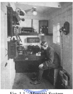
of Heinrich Rudolf Hertz and began to see the significance that wireless communication would have for the modern world. In 1894 Marconi began experimentations, and in 1899 sent a telegraphic message across the English Channel without any cables. Only three years later, Marconi’s wireless devices were able to send and receive a telegraph across the Atlantic Ocean.
Fig. 1.1 Marconi System
In the early years of Marconi’s wireless telegraphy, the main uses for it were for military purposes. The first war that Marconi’s wireless communications systems were used was the Boer War in 1899, and in 1912, a wireless device set sail with the Titanic. It was the best system in the world, and without it, the tragedy of the Titanic could have been worse, because it was the device that alerted other ships in the area of the sinking Titanic. By the 1920s, wireless telegraphy had become a mass medium, and its popularity soared with the public's discovery that it could send personal messages across continents. With the introduction of broadcast radio, wireless technology became commercially viable.
In the last thirty years wireless communication technologies have seen a revolution, as people rediscover the uses for it, and its advantages.
In the 1980s, wireless technologies were analogue signals (1G), in the 1990s they changed to digital (2G), recently they remained digital but became better quality and faster, and now the future is heading rapidly for 4G communications. In 1994, the Ericsson telecommunications company began devising and developing a technology that would connect portable devices whilst replacing cables. They named this device as Bluetooth after King Harald I of Norway, who joined Denmark and Norway. Under the aims of the Ericsson company for Bluetooth, this parallel the objective of Bluetooth technology, which aims to unite the computer and telecommunication industry. After its initial development, Ericsson realized that the product had huge potential worldwide, and from the Bluetooth Special Interest Group, which now includes over 1000 companies from around the world. The demand on today's society has seen technologies like Bluetooth becoming an extremely popular alternative to wired communications and cables.
1.3 Introduce to The Standards on
Wireless Communication System
1.3.1 Wi-Fi
Wi-Fi is short for wireless fidelity and is meant to be used generically when referring of any type of 802.11 network, whether 802.11b, 802.11a, dual-band, etc. The term is promulgated by the Wi-Fi Alliance. Any products tested and approved as "Wi-Fi Certified" (a registered trademark) by the Wi-Fi Alliance are certified as interoperable with each other, even if they are from different manufacturers. A user with a "Wi-Fi Certified" product can use any brand of access point with any other brand of client hardware that also is certified. Typically, however, any Wi-Fi product using the same radio frequency (for example, 2.4GHz for 802.11b or 11g, 5GHz for 802.11a) will work with any other,
even if not "Wi-Fi Certified."
Formerly, the term "Wi-Fi" was used only in place of the 2.4GHz 802.11b standard, in the same way that "Ethernet" is used in place of IEEE 802.3. The Alliance expanded the generic use of the term in an attempt to stop confusion about wireless LAN interoperability.
An 802.11 LAN is based on a cellular architecture where the system is subdivided into cells, where each cell (called Basic Service Set or BSS, in the 802.11 nomenclature) is controlled by a Base Station (called Access Point, or in short AP).
Even though that a wireless LAN may be formed by a single cell, with a single Access Point, (and as will be described later, it can also work without an Access Point), most installations will be formed by several cells, where the Access Points are connected through some kind of backbone (celled Distribution System or DS), typically Ethernet, and in some cases wireless itself.
The whole interconnected Wireless LAN including the different cells, their respective Access Points and the Distribution System, is seen to the upper layers of the OSI model, as a single 802 network, and is called in the Standard as Extended Service Set (ESS).
The following picture shows a typical 802.11 LAN, with the components described previously:
1.3.1 BlueTooth
In early 1998, a consortium of companies including Ericsson, IBM, Intel, Nokia, and Toshiba formed a special interest group, codenamed "Bluetooth". The group's goal was to develop a low-cost, flexible wireless platform for short-distance communication (< ~10 meters). The Bluetooth 1.0 specifications were released on July 26, 1999, but the technology has only recently become cheap enough for widespread use. The cost of a Bluetooth radio chip has dropped from $20 and is now approximately $5.
Spectrum is divided up into 79 channels spaced 1 MHz apart. Data is transmitted at 1 Mbps. For security benefits and noise reduction, a Bluetooth transmitter employs frequency hopping, switching channels up to 1600 times a second.
Bluetooth is capable of point-to-point or point-to-multipoint communication. This flexibility allows Bluetooth to be used in a wide variety of applications. Because power consumption is always a concern for mobile devices, Bluetooth has three power classes that can be used depending on how far apart the communicating devices are from one another.
In 2002 Ericsson's Bluetooth technology had finally won a standard with the IEEE global standards body, a much needed shot in the arm for the fledgling wireless Personal Area Network (PAN) technology. The standard, 802.15.1, will lend validity to Bluetooth devices, and enable vendors to better support the hardware and software involved. Bluetooth devices based on this standard will suffer fewer compatibility issues than current implementations.
The IEEE licenses part of the current standard, authored by the Bluetooth SIG, as a basis for its 802.15 standard. As a result, 802.15 devices will be fully compatible with Bluetooth v1.1 devices.
Over the next few years, Bluetooth's use is expected to significantly grow. The specifications for Bluetooth 2.0 had been finalized for a couple years. Bluetooth 2.0 had been designed to complement existing Bluetooth devices and will offer data transmission rates up to 12 Mbps.
Chapter 2
The Principal Concepts of
Designing Low Noise
Amplifier and Mixer
In this chapter, the principal concepts on designing Low Noise Amplifier and Mixer will be introduced. Since RF receiving front-end circuits usually get extremely weak signals from free space. The extremely weak signals are susceptible to noise, and always greatly affect overall performance. Therefore, before we begin to design RF receiving front-end circuits, the most important thing for us is to realize why noise is generated, and how to reduce the effect of noise. Besides, while designing each block such as LNA, mixer, we should have system view for acquiring the best overall performance. Hence, some design considerations and characteristics will be carefully taken into account in this chapter.
2.1 Introduction Noise Sources
In this subsection, only the intrinsic noises will be introduced. They are caused by small current and voltage fluctuations produced within devices themselves. The extraneous man-made signals that could be a problem in high-gain circuit will be excluded. The existence of noise is basically due to the fact that electrical charge is not continuous, and the
discrete amount is equivalent to electron charge.
The study of noise is important because it represents a lower limit to the size of electric signal that can be amplified by a circuit without significant deterioration in signal quality. Noise also results in an upper limit to the useful gain of amplifier, because if the gain is increased without limit, the output stage of the circuit eventually begins to enter saturated region.
2.1.1 Shot Noise
Shot noise is always taken place in diodes, bipolar transistors and MOSFETs, and has relations with the conduct current on them. The origin of shot noise can be seen by considering the carrier concentrations in a diode biased in forward region. An electrical file ξ exists in the depletion region and a voltage (ψ0 – V) exists between the p-type and
n-type regions, whereψ0 is the build-in potential and V is the forward
bias on the diode. The forward current of the diode I is composed of holes from the p region and electrons from n region, which have sufficient energy to overcome the potential barrier at the junction. Once the carriers have crossed the junction, they diffuse away as minority carriers.
The passage of each carrier across the junction, which can be modeled as a random event, is dependent on the carrier having sufficient energy and a velocity directed toward the junction. Thus external current I, which appears to be a steady current, contains a large number of random independent current pulses. If the current is examined on a sensitive oscilloscope, the trace appears as Fig. 2.1, where ID is the
Fig. 2.1 Diode current I as a function of time
The fluctuation in I is termed shot noise and is generally specified in terms of its mean-square variation about average value. This is written as 2
i , where
(2.1) It can be shown that if a current I is composed of a series of random independent pulses with average value ID, then the resulting noise
current has a mean-square value
(2.2) Where q is the electronic charge ( C) and is the bandwidth in hertz. This equation shows that the noise current has a
mean-square value that is directly proportional to the bandwidth x (in hertz) of the measurement. Thus a noise-current spectral density x (with units square amperes per hertz) can be defined that is
constant as a function of frequency.
2.1.2 Thermal Noise
The mechanism producing thermal noise is totally different from ID
t
Diode Current
shot noise. In conventional resistors it is due to the random thermal motion of the electrons and is unaffected by the presence or absence of direct current, since typical electron drift velocities in a conductor are much less than electron thermal velocities. Since this source of noise is due to the thermal motion of electrons, we expect that it is related to absolute temperature T. In fact thermal noise is directly proportional to T (unlike shot noise, which is independent of T), as T approaches zero, thermal noise approaches zero.
In a resistor R, thermal noise can be shown to be represented by series voltage generator as shown in Fig. 2.2a, or by a shunt current generator as in Fig. 2.2b. These representations are equivalent and
(2.3)
(2.4) Where k is Boltzmann’s constant. At room temperature
V-C. Equation 2.3 and 2.4 show that the noise spectral density is again independent of frequency and, for thermal noise, this is true up to 1013 Hz. Thus thermal noise is another source of white noise. Note that the Norton equivalent of 2.4 can be derived from 2.3 as
(2.5) A useful number to remember for thermal noise is that at room temperature (300°K), the thermal noise spectral density in a 1-KΩ resistor is V2/Hz. Another useful equivalence is that the thermal noise-current generator of a 1-K Ω resistor at room temperature is the same as that of 50μA of direct current exhibiting shot noise.
Thermal noise as described above is a fundamental physical phenomenon and is present in any linear passive resistor. This includes conventional resistors and the radiation resistance of antennas, loudspeakers, and microphones. In the case of loudspeakers and microphones, the source of noise is the thermal motion of the air
molecules.In the case of antennas, the source of noise is the black-body radiation of the object at which the antenna is directed. In all cases, (2.3) and (2.4) give the mean-square value of the noise.
Fig. 2.2 Alternative of Thermal Noise
2.1.3 Flicker Noise
Flicker noise in one of noise found in all active device, as well as in some discrete passive elements such as carbon resistors. The origins of flicker noise are varied, but it is caused mainly by traps associated with contamination and crystal defects. These traps capture and release carriers in a random fashion and the time constants associated with the process give rise to a noise signal with energy concentrated at low frequencies. Flicker noise, which is always associated with a flow of direct current, displays a spectral density of the form
(2.6) where
= small bandwidth at frequency f I = direct current
K1 = constant for a particular device
a = constant in the range 0.5 to 2 b = constant of about unity
If b = 1 in (2.6), the noise spectral density has a 1/f frequency dependence (hence the alternative name 1/f noise), as shown in Fig. 2.3. It is apparent that flicker noise is most significant at low frequencies,
although in devices exhibiting high flicker noise levels, this noise source may dominate the device noise at frequency well into the megahertz range.
Fig. 2.3 Flicker Noise spectral density versus frequency
It was noted above that flicker noise only exists in association with a direct current. Thus in the case of carbon resistors, no flicker noise is present until a direct current is passed through the resistor (however, thermal noise always exists in the resistor and is unaffected by any direct current as long as the temperature remains constant). Consequently, carbon resistors can be used if required as external elements in low-noise, low-frequency integrated circuits as long as they carry no direct current. If the external resistors for such circuits must carry direct current, however, metal film resistors that have no flicker noise should be used. The final characteristic of flicker noise that is of interest is its amplitude distribution, which is often non-Gaussian.
2.1.4 Burst Noise
Burst noise is another type of low-frequency noise found in some integrated circuits and discrete transistors. The source of this noise is not fully understood, although it has been shown to be related to the presence of heavy-metal ion contamination. Gold-doped device show very high levels of burst noise.
Burst noise is so named because an oscilloscope trace of this type f
Log scale 1/f
of noise shows burst of noise on a number (two or more) of discrete levels. The repetition rate of the noise pulses is usually in the audio frequency range (a few kilohertz or less) and produces a popping sound when played through a loudspeaker. This has led to the name popcorn noise for this phenomenon.
The spectral density of burst noise can be shown to be the form (2.7) where
K2 = constant for a particular device
I = direct current
c = constant in the range 0.5 to 2
fc = particular frequency for a given noise process
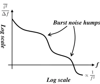
The spectrum is plotted in Fig. 2.4 and illustrates the typical hump that is characteristic of burst noise. At higher frequencies the noise spectrum falls as 1/f 2. Burst noise processes often occur with multiple
time constants, and this gives rise to multiple humps in the spectrum. Also flicker noise in invariably present as well so that the composite low-frequency noise spectrum often appear as in Fig. 2.5. As with flicker noise, factor K2 for burst noise varies considerably and must be
determined. The amplitude distribution of the noise is also non-Gaussian.
Fig. 2.4 Burst Noise spectral density versus frequency f
Log scale 1/f
Log scale
Fig. 2.5 Spectral density of combined multiple burst noise sources and flicker noise.
2.1.5 Avalanche Noise
Avalanche noise is a form of noise produced by Zener or avalanche breakdown in a pn junction. In avalanche breakdown, holes and electrons in the depletion region of a reverse-biased pn junction acquire sufficient energy to create hole-electron pairs by colliding with silicon atoms. This process is cumulative, resulting in the production of a random series of large noise spikes. The noise is always associated with a direct-current flow, and the noise produced is much greater than shot noise in the same current, as given by (2.2). This is because a single carrier can start an avalanching process that results in the production of a current burst containing many carriers moving together. The total noise is the sum of a number of random bursts of this type.
The most common situation where avalanche noise is a problem occurs when Zener diodes are used in the circuit. These devices display avalanche noise and are generally avoided in low-noise circuits. If Zener diodes are present, the noise representation of Fig. 2.6 can be used, where the noise is represented by a series voltage generator v2. The dc voltage V
z
is the breakdown voltage of the diode, and the series resistance R is f
Log scale
typically 10 to 100Ω. The magnitude of is difficult to predict as it depends on the device structure and the uniformity of the silicon crystal, but a typical measured value is V2/Hz at a dc Zener current of 0.5 mA. Note that this is equivalent to the thermal noise voltage in a 600-kΩ resistor and completely overwhelms thermal noise in R. The spectral density of the noise is approximately flat, but the amplitude distribution is generally non-Gaussian.
2.2 The Principal Concepts of Low
Noise Amplifier
In a classical radio receiver, low noise amplifier is the most significant component, owing to it dominates the sensitivity of overall system [12]. The principal concepts of designing low noise amplifier are to compromise among input impedance, noise figure, power gain, power consumptions and linearity [11]. However, there are usually some tradeoffs among them, and there is almost not one circuit achieving all goals simultaneously, especially in ultra-wide band design. Besides, different process technology will influence the difficulty of goals’ achievement. InP-BASED high electron-mobility transistor (HEMTs) provides an outstanding low-noise performance and superior high-frequency performance [18]. Moreover, HEMTs have excellent low-temperature performance, and do not have the carrier freeze-out effect even at temperature as low as 15K. However, compared with silicon technology, HEMT technology is very expensive. It is not suitable for commercial products. CMOS technology offers advantages such as low cost, mature process, good thermal conductivity, and large scale integration. However, CMOS technology suffers from high noise figure.
There are a huge number of papers published regarding low noise amplifier design. They were applying various structures for different applications. The resistive feedback amplifier [19] could easily achieve input impedance matching, yet it suffers from noise figure deterioration problem. Moreover, it usually limits input match at higher frequency due to the parasitic input capacitance [20]. The series feedback with inductive source degeneration [21-22] offers good input impedance with sufficient low noise figure, yet it is laborious for ultra-wide band design. The low noise amplifier employing an input three-section band-pass Chbyshev filter [20] can acquire wide band input impedance and low noise figure as well. However, the capacitance Cp between the gate and the source of the
input device should be chosen considering the compromise between the size of Ls and the available power gain, while large Cp leads to the gain
Below are three popular low noise amplifier structures which are widespread used in numerous products.
2.2.1 Classical Noise Matching Technique
Classical Noise Matching (CNM) Technique is used to acquiring minimum NF, Fmin, by presenting the optimum noise impedance Zopt to
the given amplifier. We usually implement this technique by placing a matching circuit between the source and input of the amplifier. By applying this technique, the LNA can be designed to achieve an NF equal to Fmin of the transistor, the lowest NF that can be obtained with the given
technology. However, due to the inherent mismatch between Zopt and Z*in
(where Z*in is the complex conjugate of the amplifier input impedance), the amplifier can experience a significant gain mismatch at the input. Therefore, the CNM technique typically requires compromise between the gain and noise performance.
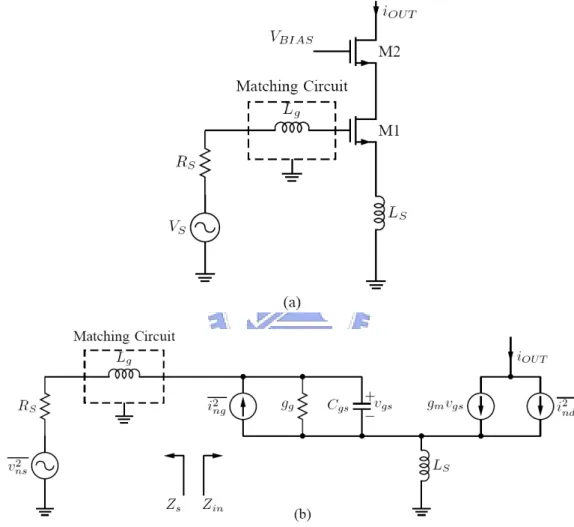
Fig. 2.7(a) shows a cascade-type LNA topology, which is one of the most popular topology due to its wide bandwidth, high gain, and high reverse isolation. In the given example, the selection of the cascade topology simplifies the analysis, and the gate-drain capacitance can be neglected.
Fig. 2.7(b) shows the simplified small-signal equivalent circuit of the cascade amplifier for the noise analysis including the intrinsic transistor noise model. In Fig. 2.7(b), the effects of the common-gate transistor M2 on the noise and frequency response are neglected, as well
as the parasitic resistances of gate, body, source, and drain terminal.
In Fig 2.7(b), represents the mean-squared channel thermal noise current, which is given by
(2.8) Where is the drain-source conductance at zero drain-source voltage VDS, k is the Boltzmann constant, T is the absolute temperature, and xx
zero VDS and 2/3 in saturation mode operation with long channel devices.
The value of γ increase at high VGS and VDS and can be more than two in
short-channel devices.
Fig. 2.7 (a)Schematic of a cascade LNA topology adopted to apply the CNM technique. (b) Its small-signal equivalent circuit.
The fluctuating channel potential due to channel noise current
shown in (2.8) couples capacitively into the gate terminal, leading to a noisy gate current. The mean-squared gate-induced noise current is given by
(2.9) where
(2.10) In (2.9), δis a constant with value of 4/3 in long-channel device,
and Cgs represents the gate-source capacitance of the input transistor. Like
γ, the value of δ also increases in short-channel devices and at high VGS and VDS . Since the gate-induced noise current has a correlation with
the channel noise current, a correlation coefficient is defined as follows: (2.11)
After some lengthy algebraic derivations, the noise parameters for the cascode amplifier shown in Fig. 2.7(1) can be expressed as
(2.12) (2.13) (2.14) where represents the noise resistance, is the optimum noise admittance, and is the minimum noise factor, respectively.
Note that, from Fig. 2.7(b), the input admittance is purely capacitive, i.e., . By comparing the complex conjugate of with (2.13), it can be seen that the optimum source admittance for input matching is inherently different from that of the noise matching in both real and imaginary part. Thus, with the given example, one cannot obtain input matching and minimum NF simultaneously. This is the main limitation of the CNM technique when applied to the LNA topology shown in Fig. 2.7(a).
2.2.2 Simultaneous Noise and Input Matching
Technique
While designing low noise amplifier, feedback techniques are always implemented in order to shift the optimum noise impedance Zopt to
the desired point. Shunt feedback has been applied for wide-band [23] and better input/output matching. Series feedback has been preferred to
obtain SNIM without the degradation of the NF. The series feedback with inductive source degeneration, which is applied to the common-source or cascode topology, is especially widely used for narrow-band applications.
Fig. 2.8(a) and (b) shows a cascade LNA with inductive source degeneration and the simplified small-signal equivalent circuit.
Fig. 2.8 (a) Schematic of a cascode LNA topology adopted to apply the SNIM technique. (b) Its small-signal equivalent circuit.
In Fig. 2.8(b), the same simplifications are applied as in Fig. 2.7(b).
The following are the ways to obtain the noise parameter expressions of a MOSFET with series feedback: noise transformation formula using noise parameters, using the noise matrix, or Kirchoff’s current las/Kirchoff’s voltage law (KCL/KVL) with noise current sources. As in (2.12)-(2.14), the noise parameters seen in the gate of the circuit shown in Fig. 2.8(b)
can be obtained. The derivation is somewhat tedious, but the result is simple enough to provide useful insights. The noise factor and noise parameters can be given by
(2.15) (2.16) (2.17) (2.18)
In (2.16)-(2.18), the noise parameters with superscripted zeros are those of the cascode amplifier with no degeneration [see (2.12)-(2.14)]. Note that (2.17) is expressed in impedance, as it is simpler in this case, and is given by
(2.19)
Note that, from (2.16)-(2.18), only Zopt is shifted and there is no
change in Rn and Fmin. Also, note that (2.16)-(2.18) are valid for any
arbitrary matching circuits, as well as the source impedance Rs in Fig. 2.8.
In addition, as shown in Fig. 2.8(b), the input impedance Zin of the given
LNA can be expressed as
(2.20) As can be seen from (2.20), the source degeneration generates the
real part at the input impedance. This is important because there is no real part in Zin without degeneration, while there is in Zopt. Therefore, if not
excessive, Ls helps to reduce the discrepancy between the real parts of
Zopt and Zin of the LNA. Furthermore, from (2.20), the imaginary part of
Zin is changed by sLs, and this is followed by the same change in Zopt, as
shown in (2.17).
For the circuit shown in Fig. 2.8(a), the condition that allows the SNIM is
(2.21) From (2.16)-(2.18) and (2.20), the conditions that satisfy (2.21) and matching with the source impedance Zs are as follows:
(2.22) (2.23) (2.24) (2.25)
As described above, based on (2.20), (2.23) and (2.24) are the same, especially in advanced technology. Therefore, (2.24) should be dropped considering the importance of the noise performance. Some amount of mismatch in the input matching has a negligible effect on the LNA performance, while the mismatch in Zopt directly affects the NF. Now then,
from (2.16)-(2.20), the design parameters that can satisfy (2.22), (2.23) and (2.25) are VGS, the transistor size W (or Cgs), and Ls. Minimum gate
length is assumed to maximize the transistor cutoff frequency ωT.
Therefore, for the given value of Zs, (2.22), (2.23) and (2.25) can be
solved since three effective equations are provided with three unknowns. The above LNA design technique suggests that, by the addition of Ls, in principle, the SNIM can be achieved at any values of Zs by
satisfying (2.22), (2.23) and (2.25) assuming (2.16)-(2.20) are valid. Many cases, especially those with large transistor size, high power dissipation, and high frequency of operation can be satisfied without much difficulty, while (2.16)-(2.20) stay valid. The problem occurs when
the transistor size is small (hence, the power dissipation is small) and the LNA operates at low frequencies. Equation (2.19) indicates that the small transistor size and/or low frequency leads to high value of Re[Zopt].
Therefore, from (2.20), for the given bias point or ωT, the degeneration
inductor Ls has to be very large to satisfy (2.25). The problem is that for
the Ls to be greater than some value, (2.18) becomes invalid and Fmin
increases significantly. As a result, the minimum achievable NF of the LNA can be considerably higher than Fmin of the common-source
transistor, spoiling the idea of SNIM. In other words, the SNIM technique is not applicable for the transistor sizes and bias levels as Re[Zopt]
becomes greater than Re[Zin] for the value of Ls, which does not degrade
the Fmin of the LNA. The inaccuracy of (2.18) for large Ls might be
caused by the negligence of Cgd. With large Ls, the transconductance of
the common-source stage can degrade significantly and the feedback signal through Cgd could become nonnegligible. As a practical design
technique, the minimum value of Ls, which does not degrade Fmin, can be
identified by monitoring the Fmin of the LNA as a function of Ls in
simulation.
2.2.3 Power-Constrained Simultaneous Noise and
Input Matching Technique
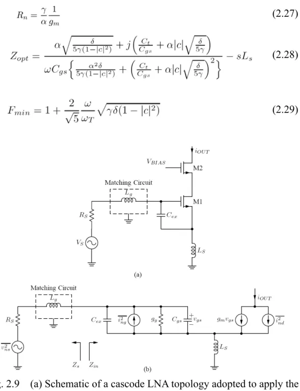
As described above, SNIM technique is not allowed at low-power implementations. However, the need for low-power implementation of a radio transceiver is one of the inevitable technical trends. Fig. 2.9(a) shows a cascoded amplifier topology that can satisfy the SNIM at low power. Note that the difference in Fig. 2.9(a) compared to the LNA shown in Fig. 2.8(a) is one additional capacitor Cex. Fig. 2.9(b) shows the
simplified small-signal equivalent circuit of Fig. 2.9(a). Again, in Fig. 2.9(b), the same simplifications are applied as in Fig. 2.7(b) and 2.8(b). The noise parameter equations can be derived by replacing (2.8) with the following expression:
(2.26) Where and . Equation (2.26) is the same expression as (2.8), but is just rewritten for simpler mathematics. The noise parameters can be given by
(2.27)
(2.28)
(2.29)
Fig. 2.9 (a) Schematic of a cascode LNA topology adopted to apply the PCSNIM technique. (b) Its small-signal equivalent circuit.
Interestingly, as can be seen from (2.27) and (2.29), the noise resistance Rn and minimum NF, Fmin, are not affected by the addition of
Cex, which is the same as the cases shown in Fig. 2.7 and Fig. 2.8. From
Fig. 2.9(b), the input impedance of the LNA can be given by
(2.30) It can now be seen that the (2.27)-(2.30) are similar to (2.16)-(2.18) and (2.20). As discussed in Section 2.2.2, (2.27)-(2.29) are valid for rather small values of Ls.
As with the LNA topology shown in Fig. 2.8(a), for the SNIM of the circuit shown in Fig. 2.9(a), (2.21) now needs to be satisfied, and that means that the conditions shown in (2.22)-(2.25) should be satisfied. From (2.28) and (2.30), (2.22)-(2.25) can be re-expressed as follows:
(2.31)
(2.32)
(2.33) (2.34) As discussed in Section 2.2.2, for the typical values of advanced CMOS technology parameters, (2.32) is approximately equal to (2.33). Therefore, (2.33) can be dropped, which means that, as in Section 2.2.2, for the given value of Ls, the imaginary value of the optimum noise
impedance becomes approximately equal to that of the input impedance with an opposite sign automatically. The design parameters that can satisfy (2.31), (2.32) and (2.34) are VGS, W (or Cgs),
Ls, and Cex. Since there are three equations and four unknowns, (2.31),
(2.32) and (2.34) can be solved for an arbitrary value of Zs by fixing the
value of one of the design parameters. Therefore, in the PCSNIM LNA design technique, by the addition of an extra capacitor Cex, the SNIM can
be achieved at any level of power dissipation.
Note that, like the case of the SNIM technique, (2.27)-(2.29) are derived assuming Ls is not very large. The validity of this assumption in a
low-power LNA can be investigated. From (2.31) and (2.34), the following approximated relation can be made:
(2.35)
Equation (2.35) indicates that Ls is a function of Ct and ωT
(which is a function of VGS). In comparison, for the SNIM technique, a
similar relation can be obtained from (2.17), (2.22) and (2.25) as
(2.36)
By comparing (2.35) and (2.36), it can be seen that, in the PCSNIM technique applied for the low-power design, where Cgs is small,
the required degeneration inductance Ls can be reduced by the addition of
Cex. In fact, by applying the PCSNIM technique to the SNIM
technique-based LNA, the required degeneration inductance Ls can be
2.3 The Principal Concepts of Mixer
Mixers are responsible for frequency translation by multiplying two signals (and possibly their harmonics). They employed in the receive path have two distinctly different inputs, called the RF port and the LO port. The RF port senses the signal to be downconverted or upconverted and the LO port senses the periodic waveform generated by the local oscillator.
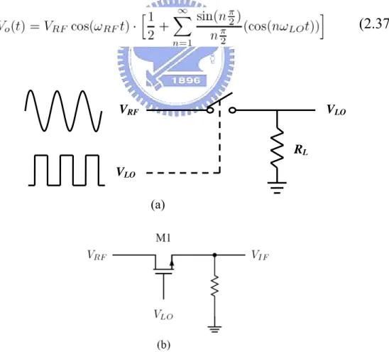
There are many ways to implement a mixer. The simplest idea is to have the LO signal turn on and off the switch in the RF path as shown in Fig. 2.10(a). In integrated circuit, an ideal switch is always implemented by a NMOS as shown in Fig. 2.10(b). For simple switch mixer, the waveform for the LO can be modeled as a return-to-zero (RTZ) square waveform. The mixer output can be modeled as
(2.37)
Fig. 2.10 (a)Simple switch used as mixer, (b)implementation of switch with an NMOS device
VRF
VLO
VLO
RL
From (2.37), it is obvious that RF component will be duplicated at upper sideband and lower sideband around LO and its odd harmonics. The upper sideband or lower sideband around LO are so-called IF components. It depends that the mixer is downconversion or upconversion. The sidebands around LO’s harmonics are not desired. Usually, they must be suppressed by filter [24] or mixer itself. The DC term in the bracket means that the RF signal is not suppressed.
2.3.1 Typical Mixer
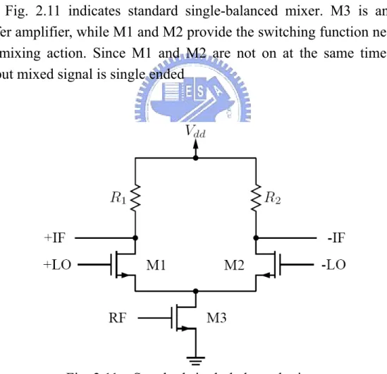
Fig. 2.11 indicates standard single-balanced mixer. M3 is an RF buffer amplifier, while M1 and M2 provide the switching function needed for mixing action. Since M1 and M2 are not on at the same time, the output mixed signal is single ended
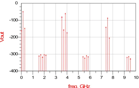
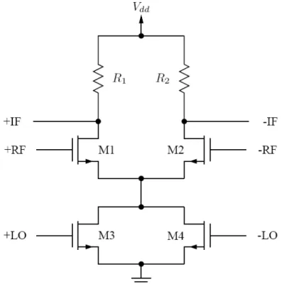
Fig. 2.12 indicates standard double-balanced mixer. The LO simply changes/modulates the phase of the RF signal between 0° and 180°. The output is never grounded. The mixing result is modeled by
(
)
⎥ ⎥ ⎥ ⎦ ⎤ ⎢ ⎢ ⎢ ⎣ ⎡ ⋅ =∑
∞ =1 ) cos( 2 ) 2 sin( ) cos( 2 ) ( n LO RF RF o n t n n t V t Vπ
ω
π
ω
(2.38)Above equation states that, in theory, by using the NRTZ switching waveform, the DC term in the equation is completely eliminated. Thus, the RF signal is greatly suppressed
1 2 3 4 5 6 7 8 9 0 10 -300 -200 -100 -400 0 freq, GHz V out
Fig. 2.13 The Simulated Result of Standard double-balanced mixer.
2.3.2 Sub-harmonic Mixer
There are three approaches to design sub-harmonic mixer. The first approach is based on a basic trigonometric equation
sin(2
ω
)=2sin(ω
)cos(ω
) (2.39) Above equation basically shows that, if the LO signal is phase-shifted by 90° and then multiplied by the original LO, twice the frequency of the LO is produced. This is exactly the property needed in a SHM. It is easily implemented by stacking another switching stage in the mixer. The non-balanced and single-balanced implementations of such a SHM are shown in Fig. 2.14 and Fig. 2.15. For the non-balanced SHM, an RC network is used to create the 90° phase shift. It is then used to drive the two switching stages of the mixer. For the single-balanced SHM, a polyphase network is used to generate the 0° and 180°, 90° and 270° signal pairs. The double-balanced version is obtained by simply cross coupling two single-balanced SHMs.Fig. 2.14 Single-ended stacked sub-harmonic mixer.
Fig. 2.15 Single-balanced stacked sub-harmonic mixer. The second generalized approach is based on yet another simple equation
Chapter 3
The Implementation of
4GHz to 20GHz Designing
Low Noise Amplifier and
Mixer
A 4HGz to 20GHz wide-band low noise amplifier is designed in Simultaneous Noise and Input Matching Technique, and fabricated in TSMC 0.18μm CMOS technology.
3.1 Induction
With much more demands on the transmission of data, voice, and video, it is urgent that the intended frequency range for the LNA needs to become wider. However, most published papers only specify the mechanism of one-pole matching for LNA. One-pole matching is difficult to achieve wide-band matching.
In this project, we would like to design an ultra-wide band low noise amplifier, which is implemented based on UMC 0.18 um CMOS technology. The frequency range of operation is from 4 to 20 GHz, and under this range the input reflection coefficient must be under -10 dB and power gain must be large than 20 dB. This design utilizes common SNIM technique, which can simultaneously achieve noise and input matching. Besides, capacitor feedback technique is also applied in the design for realizing ultra-wide band requirement.
This project is achieved on Angilent ADS. Fig. 3.1 is the input stage of wide-band low noise amplifier. Transmission lines, TL22 and TL23, are utilized to emulate the effects of inductors. Each μm transmission line has around the effect of around 1pH inductance. Basically, the structure is utilized the SNIM technique plus capacitor parallel-feedback technique. While the circuit operates at high-frequency, C20 can be considered as short circuit. The input impedance of the circuit consists of C20、T23、 T24、R1 and the input impedance of next stage, and the 50Ω input impedance can be achieved.
Fig. 3.1 The input stage of wide-band low noise amplifier.
While the circuit operates at high-frequency, owing to millier effect on C20, there is an equivalent capacitor at the gate of transistor M1. It parallel with the input capacitor of M1 Cgs, and make input match at
lower frequency. Though resistors will increase noise figure, R1 doesn’t contribute noise much. That is because it is located at the output of first stage, and the gain of first stage is not very lower. Besides, R1 is essential for increasing the stability of circuit.
Fig. 3.2 The second stage of wide-band low noise amplifier.
Fig. 3.2 is the second stage of this project. Again, it is also a common-mode source amplifier. Its gain is around 10dB.
Fig. 3.3 The third stage of wide-band low noise amplifier.
Fig. 3.3 is the third stage of this project. Again, it is also a common-mode source amplifier, too. Its gain is also around 10dB.
Fig. 3.4 The last stage of wide-band low noise amplifier.
Fig. 3.4 is the last stage of this project. Similarly, it is also a common-mode source amplifier. Its gain is also around 5dB. The output impedance matching is achieved by LC networks.
3.3 The Simulated Results
0.2 0.4 0.6 0.8 1.0 1.2 1.4 0.0 1.6 0.002 0.004 0.006 0.008 0.010 0.000 0.012 Vg=0.000 Vg=0.100 Vg=0.200 Vg=0.300 Vg=0.400 Vg=0.500 Vg=0.600 Vg=0.700 Vg=0.800 Vdd I_P rob e1. i
Fig. 3.5 The simulated DC characters of single transistor
Fig. 3.5 are the simulated DC characters of single transistor, while Vg is 0.8V voltages, Vdd is 1.5V voltage, and Id1 is around 10.5mA
5 10 15 20 25 30 35 0 40 -20 -15 -10 -5 0 5 10 15 20 -25 25 100 200 300 400 500 600 700 800 900 0 1000 freq, GHz dB(S(1, 1) ) dB(S(2, 1) ) te (2 )
Fig. 3.6 The simulated S-parameters of wide-band low noise amplifier
m1 freq= S(1,1)=0.480 / -105.859 impedance = Z0 * (0.515 - j0.619) 4.000GHz m2freq= S(1,1)=0.304 / -10.501 impedance = Z0 * (1.835 - j0.224) 20.00GHz freq (100.0MHz to 40.00GHz) S( 1, 1) m1 m2
Fig. 3.7 The simulated input reflection coefficient (S11) on Smith chart
of wide-band low noise amplifier
Fig. 3.6 and Fig. 3.7 are the simulated results on Angilent ADS. The power gain on intended frequency range is up to 22dB, reflection coefficient at input terminal is lower than -10dB, and the noise
temperature is lower than 600 degrees centigrade. 5 10 15 20 25 30 35 0 40 -20 -15 -10 -5 0 5 10 15 20 -25 25 0 20 40 60 80 100 120 140 160 180 -20 200 freq, GHz dB (S (1 ,1 )) dB (S (2 ,1 )) StabF ac t1
Fig. 3.8 The simulated stability factor of wide-band low noise amplifier
Fig. 3.8 is the simulated stability factor. Obviously, the circuit is stable on intended frequency range.
3.4 Expected Specifications
Parameters Values
Bandwidth 4-20GHz
S
21[dB]
21-22
Noise Temperature[K]
Under 300
S
11[dB] under
-10
Power dissipation[mw]
50.4
Technology[um] 0.18
Table. 3-1 The expected specifications of wide-band low noise amplifier
Power consumption is estimated while LNA operates at DC. Each transistor consumes 7mA current. Four transistors consume 50.4mW power when power supply is 1.8V.
3.5 The Layout of Wide-Band LNA
Fig. 3.9 The metal 6 of wide-band low noise amplifier layout
Fig. 3.11 The metal 4 of wide-band low noise amplifier layout
Fig. 3.13 The metal 2 of wide-band low noise amplifier layout
Fig. 3.14 The metal 1 of wide-band low noise amplifier layout Fig. 3.9 to Fig. 3.14 are the layout of wide-band low noise amplifier, have the dimension 1400 x 800 x 1200 μm and are fabricated by TSMC 0.18μm technology.
3.6 Measurement
Fig. 3.15 The testing environment at VIA RF lab.
We measured the dice by IC-cap at VIA technology LTD. Fig. 3.15 indicates the testing environments. The effective testing frequency range of RF probes and testing instruments can be up to 50GHz. While measuring, two sets of RF probes are essential. One is for input terminal, and the other is for output terminal. Besides, four DC probes are necessary for DC feeding. They are fed into Vgg1、Vgg2、Vdd1 and Vdd2
respectively. Vgg1 and Vgg2 are fed by 0.8V voltages. Vdd1 and Vdd2 are fed
by 1.5V voltages. The testing probes and dice of wide-band LNA is shown in Fig. 3.16. In order to measure the device accurately, we need to calibrate RF probe and testing instruments before measuring
3.7 Measurement Results
We first measured DC characters of the transistor on first stage. The
measured is shown in Fig. 3.17. While Vgg1 is 0.8V voltage, we could
measure that Id1 is around 9mA. Compared with simulated results, the
measured result is not out of our expectations.
Fig. 3.17 The measured DC characters of the transistor on first stage
Fig. 3.18 The measured input reflection coefficient (S11) and output
reflection coefficient (S12)
The measured input reflection coefficient (S11) and output reflection
coefficient (S12) are shown in Fig. 3.18. Due to the restriction of
instruments, we fed the port 1 of instrument into the output of device and port 2 into the input of device. Therefore, the S11 on Fig. 3.18 actually is
output reflection coefficient (S22), and S22 is the input reflection
coefficient (S11). From Fig. 3.18, we found that the measured results are
far from like the simulated results. S11 is not lower than -10dB in intended
Fig. 3.19 The measured forward transmission coefficient (S21) and
reverse transmission coefficient (S12)
The measured forward transmission coefficient (S21) and reverse
transmission coefficient (S12) are shown in Fig. 3.19. Similarly, due to the
restriction of instruments, we fed the port 1 of instrument into the output of device and port 2 into the input of device. Therefore, the S21 on Fig.
3.19 actually is reverse transmission coefficient (S12), and S12 is the
forward transmission coefficient (S21). The measured forward
transmission coefficient (S21) is around -22dB to -16dB. Compared with
simulated result, there are a lot of differences.
3.8 Conclusion For Wide-Band LNA
The chip malfunctions, and we have some ideas which might be the root causes.
A. The issues on layout
In this project most components are placed on metal 6, and metal 2 to metal 5 are placed on ground plane. Owing to there are 0.8μm gap
between metal 5 and metal 6, it will result in much effects of parasitic capacitor under many transmission lines which are utilized to imitate inductors. It makes the character of whole circuit greatly change. Therefore most places on metal 2 to metal 5 should be reserved.
B. The issues on the settings of ADS
While simulating on ADS, some parameters about substrate are not correctly set, such as the height of substrate. Owing to metal 5 is placed on ground plane, the correct height of substrate is 0.8μm. Besides, the dielectric constant is set wrong, too. Though, it won’t greatly change input reflection coefficient, it will make power gain not to be so flat any more under intended frequency range. After changing wrong parameters to correct ones and simulating again, we found the simulated results are very like to measured results. The simulated results are shown Fig. 3.20.
C. The issues on components placement
In our design, we utilize many components provided by wafer company. The places under inductor, between metal 2 to metal 5, shouldn’t be placed ground plane. It doesn’t make the characters of components consist with the ones provided by wafer company. Besides, after completing simulation on ADS, it is essential to run Momentum to verify the characters of inductors and transmission lines. The works on running Momentum are omitted.
5 10 15 20 25 30 35 0 40 -25 -20 -15 -10 -5 0 5 10 15 20 -30 25 100 200 300 400 500 600 700 800 900 0 1000 freq, GHz dB (S (1 ,1 )) dB (S (2 ,1 )) te (2 )
Fig. 3.20 The simulated input reflection coefficient (S11) and output
reflection coefficient (S12) after changing wrong parameters to correct
ones
D. The issues on transmission lines
The places under inductor, between metal 2 to metal 5, shouldn’t be placed ground plane, and we should place ground place on right metal refer to the height of substrate. Besides, we should run Momentum to verify the characters of transmission lines.
E. We should consider testing environments before designing circuit
While designing circuit, we place two 300μm bond wires at input and output terminals. However, while measuring, there is no bond wire in the circuit. Though it won’t change the character a lot, we should consider testing environments before designing circuit.
Chapter 4
The Design of Novel Mixer
4.1 Induction
The intermodulation performance of a receiver front end is often limited by that of the mixer. This is because the mixer performance is usually worse than that of the other stages, and the mixer must handle the largest signal levels. Consequently, in most low-noise capability can do much to improve dynamic range.
The most commonly used mixers in microwave systems employ Schottky-barrier diodes as the mixing elements. These are usually used in balanced structures to separate the RF and local oscillator (LO) signals, to improve large-signal capability, and to reject certain even-order spurious responses and intermodulation products. Because the Schottky diode is very strongly nonlinear, diode mixers have at best mediocre intermodulation susceptibility.
Nowadays the most popular used topology of mixer is Gilbert Cell. Many papers discussing Gilbert Cell are published on international journals. In the chapter, we propose a novel mixer which is never published in worldwide international papers.
4.2 Operating Principle
Mixers are conventionally realized by applying a large LO signal and a small RF signal to a nonlinear device, usually a Schottky-barrier diode. The LO modulates the junction conductance at the LO frequency, allowing frequency conversion. In principle, this conductance could be
realized via a time-varying linear conductance, rather than a nonlinear one, resulting in a mixer without intermodulation. A simple examples of such a time-varying linear element, which is capable of intermodulation-free mixing, is an ideal switch, operated at the LO frequency, in series with a small resistor.
Fig. 4.1 shows a conventional very low intermodulation mixer(VLIM). To realize a mixer, the MOS is operated in common-source configuration, the LO is applied to the gate, with proper DC bias, and the RF is applied to the drain. The IF is filtered from the drain. The relatively large value of Cgd would couple the RF and LO
circuits to an unacceptable degree, so for a single-device mixer, RF and LO filters must be used. It is important that the LO voltage not be coupled to the drain terminal; if it is, the drain voltage will traverse the more strongly nonlinear portion of the V/I curve, increasing the IM level. The RF filter should therefore be designed to short-circuit the drain at the LO frequency. The design goal for the LO filter is not so clear. If RF voltage is coupled to the gate, it is conceivable that intermodulation could be increased because of the nonlinearities in Gm. If the gate is shorted at
the RF frequency, no RF voltage appears on the gate, so there is no possibility of IM generation in this way. However, open-circuiting the gate effectively halves the capacitance in parallel with the channel resistance, so conversion loss should be lower. In the mixer described here, the LO filter was designed to short-circuit the RF at the gate.
Fig. 4.1 Conventional very low intermodulation mixer m1 freq= dBm(Vif)=-58.7631.500GHz 5 10 15 20 25 30 35 40 45 0 50 -130 -110 -90 -70 -50 -30 -150 -10 freq, GHz dB m (Vi f) m1
Fig. 4.2 The simulated spectrum of conventional VLIM when FLO is
8.8GHz and FRF is 10.3GHz without LO and RF filters
Conventional VLIM has many advantages. The most one is simple, and the others are no DC power consumption, no 1-dB compression point since it is a passive circuit. However, the LO and RF filters are essential for reducing intermodulation, such as shown in Fig. 4.2.
intermodulation mixer. Compared with conventional VLIM, its advantage is that LO and RF filters are not needed. The LO and RF signals would be eliminated by the symmetrical architecture.
4.3 Simulated Results
m1
freq=
Vout=-20.113
1.500GHz
m3
freq=
Vout=-345.264
8.800GHz
5 10 15 20 25 30 35 40 45 0 50 -300 -200 -100 -400 0 freq, GHz Vo utm1
m3
Fig. 4.4 The output spectrum when FLO is 8.8GHz and FRF is 10.3GHz
5.0E9 1.0E10 1.5E10 2.0E10 2.5E10
0.0 3.0E10 -8 -6 -4 -2 0 -10 2 Freq_RF Conv er G ain
-70 -60 -50 -40 -30 -20 -10 0 -80 10 -60 -40 -20 0 20 -80 40 Power_RF Co nv er G ain
Fig. 4.6 Conversion gain v.s. RF power when IF is 150MHz
-70 -60 -50 -40 -30 -20 -10 0 -80 10 -60 -40 -20 0 -80 20 Power_RF Po w erI F _re al
4.4 Conclusions For Double Balance
VLIM mixer
A novel architecture of mixer is proposed. Its advantages are no DC power consumption, no RF and LO filters, and no 1-dB compression point since it is a passive mixer.