國立交通大學
電子工程學系 電子研究所碩士班
碩士論文
多層閘極介電層之奈米尺度薄膜電晶體之研究
Study on Nano-scaled Poly-Si Thin-Film Transistor
with Stacked Gate Dielectric.
研 究 生 : 蔡 佳 州
指導教授 : 施 敏 博士
張 鼎 張 博士
多層閘極介電層之奈米尺度薄膜電晶體之研究
Study on Nano-Scaled Poly-Si Thin-Film Transistor
with Stacked Gate Dielectric
研 究 生: 蔡 佳 州
Student:
Chia-Chou
Tsai
指導教授: 施 敏 博士
Advisor:
Dr.
Simon
M.
Sze
張 鼎 張 博士
Dr. Ting-Chang Chang
國 立 交 通 大 學
電子工程學系 電子研究所
碩 士 論 文
A Thesis
Submitted to Department of Electronics Engineering & Institute of Electronics
College of Electrical Engineering and Computer Science
National Chiao Tung University
in Partial Fulfillment of the Requirements
for the Degree of
Master
in
Electronics Engineering
June 2006
Hsinchu, Taiwan, Republic of China
多層閘極介電層之奈米尺度薄膜電晶體之研究
研究生: 蔡佳州
指導教授:
施 敏博士
張鼎張博士
國立交通大學
電子工程學系 電子研究所碩士班
中文摘要
在此論文中,我們首先提出了多層閘極介電質結合奈米線多通道的
薄膜電晶體之結構,此結構具有高性能薄膜電晶體的特性,另一方面,
也同時具有非揮發性記憶體的特性。
在薄膜電晶體方面,我們利用 ONO 多層閘極介電質來調配閘極介
電質的介電常數,在不減少薄膜厚度的情況下,提高閘極的控制能力;
另一方面,我們同時利用奈米線在邊緣處的曲率半徑較小,在相同電
壓下,有較大的電場之特性,製作出多通道奈米線的薄膜電晶體,可
以有效的降低導通電壓(threshold voltage),增加開關電流比(On/Off
ratio),較陡峭的次臨界導通斜率(subthreshold slope),和更優良的元
件驅動能力,其電性較一般標準結構的薄膜電晶體為好。
在非揮發性記憶體方面,由於奈米線在邊緣處具有較大的電場,可
以使元件在進行寫入/抹除(Program/Erase)的操作時,具有較高的效
率,另一方面,奈米線結構的非揮發性記憶體,無論是在資料的保存
性(Reliability)方面,或是多次讀寫(Endurance)方面,都具較好的元件
可靠度。
多層閘極奈米線薄膜電晶體有極大的潛力應用在面版上的系統整
合,利用多層閘極介電質薄膜電晶體同時具有高效能驅動元件及非揮
發性記憶體元件的特性,可以大幅的簡化製程步驟。
Study on Nano-Scaled Poly-Si Thin-Film Transistor
with Stacked Gate Dielectric
Student: Chia-Chou Tsai Advisors: Dr. Simon M. Sze
Dr. Ting-Chang Chang
Department of Electronics Engineering &
Institute of Electronics
National-Chiao-Tung-Unversity
Hsinchu
Taiwan
Abstract
In this thesis, we have proposed and fabricated the SONOS-TFT with nanowire structure. The SONOS-TFTs can be used on the high performance driving device application and nonvolatile memory device application.
For driving device application, we have used multilayer ONO gate dielectrics to make change the effective dielectric constant. The proposed TFT with ONO gate dielectrics have better gate control ability. On the other hand, nanowire has larger electric-field in the corner region at the same voltage. The SONOS-TFT with multiple nanowire channels have superior electrical characteristic, such as lower threshold voltage, higher On/Off ratio, steeper subthreshold slope, and superior driving ability.
In nonvolatile memory application, the SONOS-TFT with nanowire structure have superior program / erase efficiency for its higher electric field near the corner region. On the other hand, SONOS-TFT with nanowire structure have better reliability, either retention or endurance.
The SONOS-TFTs combined the TFT and memory properties at the same time. Furthermore, the process flow is compatible with conventional poly-Si TFTs fabrication without additional process steps. Hence, the application of SONOS TFTs structure can reach the goal of system on panel (SOP) in the future.
誌謝
兩年的碩士班生活,轉瞬間就過去了,在這段時間裡所認識的老師、學長、 同學、學弟妹以及朋友們,雖然我們相處的時間不長,但謝謝你們的在身旁陪伴 我,度過這段美麗的時光。 一開始,最感謝的還是我的指導教授,施敏老師以及張鼎張老師,很幸運的 能夠成為你們的學生,學到老師對一件事情嚴謹的態度,對問題所提出精闢的見 解,圓融的處世,讓學生獲益良多,能夠成為你們的學生,真是我莫大的福氣。 接下來,要感謝的是交通大學奈米中心以及國家奈米元件實驗室,有優良的 實驗設備,才有辦法提供學生有良好的實驗結果。在實驗上一起奮鬥的伙伴們: 土撥學長及世青學長,有你們,這篇論文才能順利完成,還有秉宏、陳董、國王、 大山、立偉這幾位學長,星舟、緯仁、林博、阿貴、淵州和俐婷、勝凱(還是叫本 名好了),睿龍、小馬、老胡,還有其它 TCC Group 的同伴們,有你們的陪伴,實 驗的路上一向都不孤單。 其它要感謝的人,如奈米中心的何小姐,提供我在校內工讀的機會,還有大 同及台科大的同學,以及實驗室以前的學長們,偶爾跟你們在路邊攤把酒言歡, 在笑傲江湖唱歌發洩,實在是令人懷念,願友情永遠存在。 在新竹這段時間,認識的人實在是太多了,幾個字實在是無法表達心中的感 謝,雖然有許多人被漏掉了,並不代表我對你們的感謝也因此而漏掉。 最後要感謝我的家人,媽媽,蕭芬蓉女士以及兩個妹妹,如宜和宜庭,有妳 們在背後的支持與鼓勵,讓我能夠自由選擇自己未來的方向,以及順利的完成學 業,沒有妳們,就沒有今天的我,趁著寫誌謝的同時,把這篇論文獻給妳們,希 望能把我的榮耀跟妳們一起分享。 佳 州 2006 年 6 月Contents
Chinese Abstract I
English Abstract III
Acknowledgement (Chinese) V
Contents VI
Figure Captions VIII
Table Captions XI
Chapter 1. Introduction 1
1-1. Introduction of the polycrystalline silicon thin-film transistor 1 1-2. Introduction of nonvolatile memory technology 3
1-3. Motivation 5
1-3-1. For driving device 5
1-3-2. For nonvolatile memory device 7
1-4. Thesis scheme 8
Chapter 2. SONOS-TFT for driving device application 12
2-1. The fabrication of SONOS-TFT 12
2-2. Carrier transport mechanism of poly-Si TFTs 15
2-3. Method of device parameter extraction 19
2-3-1. Determination of the threshold voltage 19 2-3-2. Determination of the subthreshold swing 19 2-3-3. Determination of On/Off current ratio 20 2-3-4. Determination of the field-effect mobility 21
2-4. Results and discussion 22
2-5. Summary 26
Chapter 3. SONOS-TFT for nonvolatile memory application 35
3-1. The fabrication of SONOS-TFT 35
3-2. The program/erase mechanism 35
3-2-1. Hot electron injection 36
3-2-2. Tunneling injection 37
3-3. Retention and endurance for nonvolatile fresh memory 38
3-3-1. Retention 38
3-3-2. Endurance 40
3-4. The electrical characteristics of SONOS-TFT with multiple
nanowire channels. 42
3-4-1. Program / erase characteristics 42
3-4-2. Retention 43
Chapter 4. Conclusion 60 References
Figure captions
Chapter 1.
Fig. 1-1 The structure of the conventional floating gate nonvolatile memory device. Continuous poly-Si floating gate is used as the charge storage element and ONO sandwiched structure is used as the control oxide. Fig. 1-2 The structure of the SONOS nonvolatile memory device. The nitride
layer is used as the charge-trapping element.
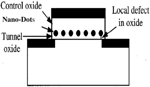
Fig. 1-3 The structure of the nanocrystal nonvolatile memory device. The semiconductor nanocrystals or metal nano-dots are used as the charge storage element instead of the continuous poly-Si floating gate.
Chapter 2.
Fig. 2-1 The schematic plot of SONOS-TFT. Fig. 2-2 The standard poly-Si TFT.
Fig. 2-3 The top view of the NW SONOS-TFT structure.
Fig. 2-4 The scanning electron microscopy (SEM) photography of the poly-Si active region of the NW SONOS-TFT.
Fig. 2-5 The transmission electron microscopy (TEM) of the 65nm nanowire channel and the ONO stacked layer in the NW SONOS-TFT.
Fig. 2-6 A schematic MOSFET cross section, showing the axes of coordinates and the bias voltages at the four terminals for the drain-current model. Fig. 2-7 ID-VG transfer characteristics of standard poly-Si TFT with TEOS oxide
gate dielectric and the proposed TFT (SONOS-TFT) with ONO stack gate dielectric.
numbers of channels with different widths.
Fig. 2-9 The maximum normalized drain current of the SONOS-TFTs and the standard TFTs versus the different structures at VD = 5V.
Fig. 2-10 The threshold voltage (Vth) of the SONOS-TFTs and standard TFTs
versus the multiple channels with different widths.
Fig. 2-11 The sub threshold swing (S.S.) of the SONOS-TFTs and standard TFTs versus the multiple channels with different widths.
Fig. 2-12 ID-VD curves of the SONOS-TFTs versus the multiple channels with
different widths at VGS = 6 V. Fig. 2-12 ID-VD curves of the
SONOS-TFTs versus the multiple channels with different widths at VGS
= 6 V.
Fig. 2-13 ID-VD curves of the standard TFTs and SONOS-TFT with S1 and NW
TFT structures.
Chapter 3.
Fig. 3-1 I–V curves of an FG device when there is no charge stored in the FG (curve A) and when a negative charge is stored in the FG (curve B). Fig. 3-2 Schematic cross section of MOSFET. The energy- distribution function
at point X1; Y1 is also shown
Fig. 3-3 Fourth approaches to programming methods.
Fig. 3-4 Bandgap diagram of a SONOS device in the excess electron state, showing retention loss mechanisms: trap-to-band tunneling (TB), trap-to-trap tunneling (T-T), band-to-trap tunneling (B-T), thermal excitation (TE) and Poole–Frenkel emission (PF)
on a single cell.
Fig. 3-7 Anomalous SILC modeling. The leakage is caused by a cluster of positive charge generated in the oxide during erase.
Fig. 3-8 (a) The transfer ID-VG curves of S1 structures with the different program
time at a 15V program voltage.
Fig. 3-8 (b) The transfer ID-VG curves of NW structures with the different program
time at a 15V program voltage.
Fig. 3-9 (a) The transfer ID-VG curves of S1 structures with the different program
time at a 20V program voltage.
Fig. 3-9 (b) The transfer ID-VG curves of NW structures with the different program
time at a 20V program voltage.
Fig. 3-10 The program characteristics of NW and S1 SONOS-TFTs with different gate voltage.
Fig. 3-11 The erase characteristics of NW and S1 SONOS-TFTs with different gate voltage.
Fig. 3-12 Programming voltage is 20V for 2s. It is clear that the memory window loss of NW SONOS-TFT is lower than 0.5V after extrapolating to retention time of 10 years and still kept about 3V.
Fig. 3-13 (1)Electrons injected from channel via tunneling through the tunnel oxide. (2)Some of the injected electrons are captured by the traps of the nitride.(either deep traps or shallow traps) (3)The thermal excitation electrons may detrap from trapping states and move to blocking oxide by the field-enhanced Poole-Frenkel (P-F) emission. (4)At the high temperature, electrons captured in shallow traps can easily detrap and be drawn out in the high electric field.
cycles.
Fig. 3-14 (b) present the transfer ID-VG curves of NW structures with various P/E
cycles.
Fig. 3-15 The SONOS-TFT with nanowire structure maintains a 3V Vth window
after 106 P/E cycles.
Table captions
Chapter 1
Introduction
1-1. Introduction of the Polycrystalline Silicon Thin-Film
Transistor
In recent years, polycrystalline silicon (poly-Si) thin film transistors (TFTs) have drawn much attention because of their applications in active matrix liquid crystal displays (AMLCDs)[1] and organic light emitting diodes (OLEDs)[2]. Lately, some superior performances of poly-Si TFTs also have been reported by scaling down device dimensions or utilizing novel crystallization technologies to enhance poly-Si film quality[3.4]. This provides opportunity of using poly-Si TFTs in three-dimensional (3D) integrated circuit fabrication, such as Fresh memory. However, the application in AMLCDs and OLEDs is the major reason for the rapid programs in poly-Si TFT technology.
The poly-Si TFTs are currently investigated for applications in active matrices for LCD. The possibility of integrating on the same substrate driving circuitry as well as switching devices represents a major advantage of the polysilicon technology over the amorphous silicon, because the mobility of
poly-Si TFTs is usually large than 10 cm2/V-s, that is high enough for peripheral
driving circuits with n- and p-channel devices. The pixel array and the peripheral circuits can be made on the same glass substrate [5-7], a potential system-on-panel (SOP) technology. This approach will reduce both the fabrication and the assembly costs. In addition, due to higher mobility, the poly-Si TFTs can be made smaller compared to that of the amorphous Si TFTs. High resolution AMLCDs and the aperture ratio in TFT array can be significantly improved by using poly-Si TFTs as pixel switching elements. This is because the device channel width can be scaled down while meeting the same pixel driving requirements in amorphous TFT AMLCDs.
In CMOS technology, many high-performance surrounding gate structures in a silicon-on-insulator (SOI) MOSFET, such that double-gate [8], tri-gate [9], FinFET [10] and gate-all-around [11], have been reported to exhibit superior gate control over the channel than a conventional single-gate MOSFET and reduced short-channel effects.
1-2. Introduction of Non-volatile Memory Technology
of the magnetic-core memory, the electronic industries urgently needed a new kind of memory device to replace the magnetic-core memory. In 1967, D. Kahng and S. M. Sze invented the floating-gate (FG) nonvolatile semiconductor memory at Bell Labs [12]. To date, the stacked-gate FG device structure, as shown in Fig. 1-1, continues to be the most prevailing nonvolatile-memory implementation, and is widely used in both standalone and embedded memories. The invention of FG memory impacts more than the replacement of magnetic-core memory, and creates a huge industry of portable electronic systems, such as cellular phones, digital cameras, digital voice records, personal data assistants, MP3 walkmans etc. The most widespread memory array organization is the so-called Flash memory, which has a byte-selectable write operation combined with a sector “flash” erase. They even may eventually replace the ubiquitous magnetic memory media and RAMs (Random Access Memories) in many compact electric applications.
Although a huge commercial success, conventional FG devices have their limitations. The most prominent one is the limited potential for continued scaling of the device structure. This scaling limitation stems from the extreme requirements put on the tunnel oxide layer. On the one hand, the tunnel oxide has to allow quick and efficient charge transfer to and from the FG. But the tunnel
oxide needs to provide superior isolation under retention, endurance, and disturbed conditions in order to maintain information integrity over periods of up to a decade. Once the tunnel oxide has a leaky path, all the stored charge in the floating gate will be lost. When the tunnel oxide becomes thinner, the retention characteristics will be degraded since the retention must be more then ten years, the tunnel oxide usually must thicker than 7nm. When the tunnel oxide is made thicker to take the isolation into account, the speed of the operation will be slower. Therefore, there is a tradeoff between speed and reliability, and the thickness of the tunnel oxide is compromised to about 8-11 nm, which is barely reduced over more than five successive generations of the industry [13].
To overcome the scaling limits of the conventional FG structure, two candidates are mostly mentioned, SONOS [14-16] and nanocrystal nonvolatile memory devices [17-19]. As for SONOS in Fig. 1-2, the nitride layer is used as the charge-trapping element. The intrinsic distributed storage is an advantage of the SONOS device over the FG device. It has improved endurance, since a single defect will not cause the discharge of the memory [16]. Tiwari et al. [17] were the first to demonstrate the Si nanocrystal floating gate memory device in the early nineties. As shown in Fig. 1-3, a local leaky path will not cause the fatal loss of information for the nanocrystal nonvolatile memory device. Also, the
nanocrystal memory device can maintain good retention characteristics when tunnel oxide is thinner than 7nm [17-19].
1-3. Motivation
1-3-1 For driving device
Poly-Si TFTs have drawn great attentions for its application on active-matrix liquid-crystal-displays (AMLCDs) for its high field effect mobility and driving current. Also, the poly-Si TFTs are also promising to be integrated with peripheral driving circuits on a low-cost glass substrate [1], [20]. In addition, poly-Si TFTs have the potential to be used in three-dimensional (3D) circuits, including vertically integrated SRAMs [21] and DRAMs [22]. However, the improvement of electrical characteristics and the reduction of undesirable effect are still important issues. It was reported that using high dielectric constant materials as gate insulator can improve the device performance [23]. However, using high dielectric constant materials, such as silicon nitride causes poor interface between the nitride/poly-Si layers to degrade the device performance. In 1984, the first report of the oxide-nitride-oxide (ONO) multilayer was used as alternative dielectrics for DRAM cell capacitor [24]. In 1995, the poly-Si TFT used
the high dielectric constant ONO multilayer as a gate insulator was reported [25] to solve the above problem. In the ONO multilayer, the nitride layer is used to increase the effective dielectric constant and the other oxide layers are used to provide the electrical contact in the SiO2/poly-Si interface. Recently, poly-Si TFTs
adopting multiple nanowire channels structure was reported for highly improved poly-Si TFTs performance [26], [27].
In this thesis, we combine ONO gate dielectric and a series of multiple channel structures on poly-Si TFTs to study their effects on device performances. Also, the standard TFTs with the same thickness of oxide dielectric was fabricated for comparison. Experimental results show that the electrical characteristic of silicon-oxide-nitride-oxide-silicon thin-film transistors (SONOS-TFTs) was enhanced, comparing to standard TFTs.
1-3-2 For nonvolatile memory device
The SONOS memory elements are the charge traps distributed throughout the volume of the Si3N4 layer that stores both electrons and holes (positive
charges) injected from the channel. During programming, the control gate is biased positively so electrons from the channel can tunnel across the SiO2 into
through the control oxide, and into the control gate. The remaining electrons are trapped in the nitride layer. The trapped charges provide the electrostatic screening of the channel from the control gate. They produce the same Vth shifts
as in conventional floating gate devices.
In this thesis, we fabrication the SONOS on SiO2 and combine the multiple
nanowire channels structure. SONOS-TFT structure can be used in system-on-panel (SOP) and the 3D staked memory devices. In SOP, SONOS-TFT can have the driving and memory characteristic in different operation voltage, the structure can let the fabrication in SOP become simple; in memory, SONOS-TFT can increase the memory-cell density without scaling down the dimension of the device.
1-4. Thesis Scheme
Chapter 1. Introduction
1-1. Introduction of polycrystalline silicon thin-film transistors 1-2. Introduction of Non-volatile memory technology
1-3-1. For driving device
1-3-2. For nonvolatile memory device 1-4. Thesis scheme
Chapter 2. SONOS-TFT for driving device application 2-1. The fabrication of SONOS-TFT
2-2. Carrier transport mechanism of poly-Si TFTs 2-3. Methods of device parameter extraction
2-3-1. Determination of the threshold voltage 2-3-2. Determination of the subthreshold slope 2-3-3. Determination of On/Off Current Ratio 2-3-4. Determination of the field-effect mobility 2-4. Results and discussion
2-5. Summary
Chapter 3. SONOS-TFT for memory application 3-1. The fabrication of SONOS-TFT
3-2. The program/erase mechanism 3-2-1. Hot-electron injection 3-2-2. Tunneling injection
3-3-1. Retention
3-3-2. Endurance
3-4. The electric characteristics of SONOS-TFTs with multiple nanowire channels. 3-4-1. Program/erase characteristic 3-4-2. Retention 3-4-3. Endurance 3-5. Summary Chapter 4. Conclusion References
Fig. 1-1 The structure of the conventional floating gate nonvolatile memory device. Continuous poly-Si floating gate is used as the charge storage element and ONO sandwiched structure is used as the control oxide.
Fig. 1-2 The structure of the SONOS nonvolatile memory device. The nitride layer is used as the charge-trapping element.
Nano-Dots
Fig. 1-3 The structure of the nanocrystal nonvolatile memory device. The
semiconductor nanocrystals or metal nano-dots are used as the charge storage element instead of the continuous poly-Si floating gate.
Chapter 2
SONOS-TFT for Driving Device Application
2-1. The Fabrication of SONOS-TFT
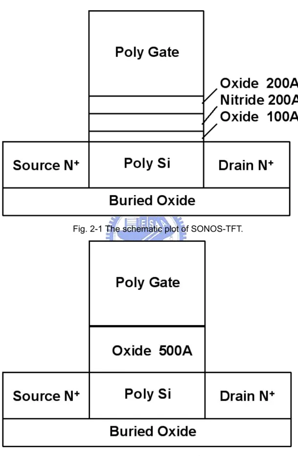
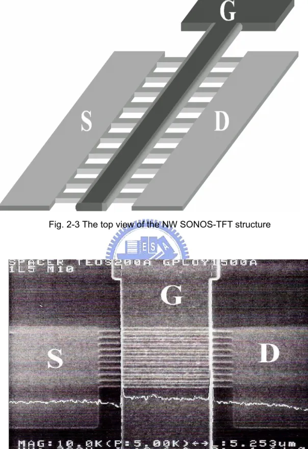
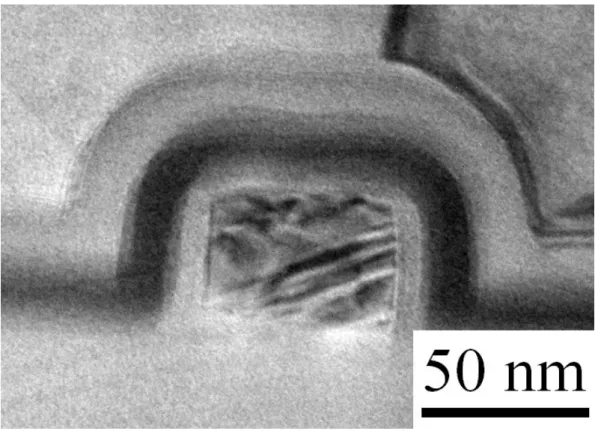
In this work, a series of SONOS-TFTs with multiple channel nanowire will be fabricated. The gate length is 5μm, consisting of ten stripes of multiple 65 nm nanowire (NW) SONOS-TFT, five stripes of multiple 0.2μm channels (M5) SONOS-TFT, two stripes of multiple 0.5μm channels (M2) SONOS-TFT and a single-channel (S1) SONOS-TFT with 1μm, were fabricated. The control sample, the standard TFTs with oxide dielectric was also prepared for comparison. Figure 2-1 presents the schematic plot of SONOS-TFT and Fig. 2-2 presents the TFT with oxide gate dielectric. The top view of the NW SONOS-TFT structure is shown in Fig 2-3. Figure 2-4 presents the scanning electron microscopy (SEM) photography of the poly-Si active region of the NW SONOS-TFT. Figure 2-5 presents the transmission electron microscopy (TEM) of the 65nm nanowire channel and the ONO stacked layer in the NW SONOS-TFT.
Step1. Substrate
as the starting substrate. After a standard cleaning procedure of the silicon wafers, a 400-nm-thick SiO2 was thermally grown in steam oxygen ambient at
1000ºC.
Step2. Poly-Si thin film formation
Undoped 50-nm-thick amorphous-Si layers were deposited by low pressure chemical vapor deposition (LPCVD) at 550ºC. The amorphous-Si films were recrystallized by solid phase crystallization (SPC) method at 600ºC for 24hrs in N2 ambient. After electron beam direct writing and transferred by reactive ion
etching (RIE), the device active region source, drain and multiple channels were formed.
Step3. Gate dielectric formation
After defining the active region, the wafers were cleaned in H2SO4/H2O2 and
NH4OH/H2O2 solution to remove residue of polymer before gate dielectric
deposition. A buffered HF dip was performed to remove the native oxide on the silicon surface. A total 50 nm-thick ONO multilayer gate dielectric, 10-nm-thick layer of tetra-ethyl-ortho-silicate (TEOS) bottom oxide was deposited by LPCVD at 700ºC, 20-nm-thick layer of silicon nitride high k dielectric was deposited by LPCVD at 780ºC, 20-nm-thick layer of TEOS top oxide was deposited by LPCVD at 700ºC. The standard TFT has 50 nm-thick TEOS oxide layer
deposited by LPCVD at 700ºC. The thickness of gate oxide was determined by N&K optical analyzer.
Step4. Gate electrode formation
After deposition of gate insulators, 150-nm-thick poly-silicon films were formed immediately on the gate insulators by LPCVD at 620°C. The second poly-Si layers were patterned by E-beam lithography and transformer couple plasma (TCP) etching to define the gate electrode and to serve as the mask for self-aligned implantation.
Step5. source/drain formation
After the gate definition, the self-aligned source and drain regions were formed by phosphorous ions implantation at a dosage of 5×1015 cm-2. After the
source and drain formation, doping activation was performed by rapid thermal anneal (RTA) at 900°C for 30s, in nitrogen ambient.
Step6. Passivation layer and contact hole formation
After source and drain implantation, a 300 nm-thick TEOS oxide layer was deposited as the passivation layer by LPCVD at 700ºC. The 10×10 um2 contact
holes were patterned by reactive ion etching (RIE) subsequently. Step7. Metallization
deposition (PVD) and then patterned to form the gate, source and drain contact metal pads. Finally, the devices were sintered at 400°C in forming-gas ambient for 30 min.
2-2. Carrier Transport Mechanism of Poly-Si TFTs
As mentioned in Section 1-1, the device characteristics of poly-Si TFTs are strongly influenced by the grain structure in poly-Si film. Even though the inversion channel region is also induced by the gate voltage as in MOSFETs, the existence of grain structure in channel layer bring large differences in carrier mobility. Many studies on the electrical properties and the carrier transport mechanism in poly-Si TFTs have been reported. A simple grain boundary-trapping model has been described by many authors in details.[1-8] In this model, it is assumed that the poly-Si material is composed of a linear chain of identical crystallite having a grain size and the grain boundary trap density ( ). The charge trapped at grain boundaries is compensated by oppositely charged depletion regions surrounding the grain boundaries. From Poisson’s equation, the charge in the depletion regions causes curvature in the energy bands, leading to potential barriers that impede the movement of any
g L
t
remaining free carriers from one grain to another. When the dopant/carrier density is small, the poly-Si grains will be fully depleted. The width of the grain boundary depletion region extends to be on each side of the boundary, and the barrier height can be expressed as
n d x Lg/2 B V s g d s B qnL x qn V ε ε 8 2 2 2 = = (2-1)
As the dopant/carrier concentration is increased, more carriers are trapped at the grain boundary. The curvature of the energy band and the height of potential barrier increase, making carrier transport from one grain to another are more difficult. When the dopant/carrier density increases to exceed a critical value , the poly-Si grains turn to be partially depleted and excess free carriers start to spear inside the grain region. The depletion width and the barrier height can be expressed as
g t L N N* = / n N x t d 2 = (2-2) n qN n N qn V s t t s B ε ε 8 2 2 2 2 = ⎟ ⎠ ⎞ ⎜ ⎝ ⎛ = (2-3)
The depletion width and the barrier height will decrease with increasing dopant/carrier density, leading to improved conductivity in carrier transport.
The carrier transport in fully depleted poly-Si film can be described by the thermionic emission over the barrier. Its’ current density can be written as[8]
⎥⎦ ⎤ ⎢⎣ ⎡− − = cexp (VB Vg) kT q qnv J (2-4)
where n is the free-carrier density, vc is the collection velocity
(
*)
2 / m kT
vc = π ,
is the barrier height without applied bias, and is the applied bias across the grain boundary region. For small applied biases, the applied voltage divided approximately uniformly between the two sides of a grain boundary. Therefore, the barrier in the forward-bias direction decreases by an amount of . In the reserve-bias direction, the barrier increases by the same amount. The current density in these two directions then can be expressed as
B V Vg 2 / g V ⎥ ⎦ ⎤ ⎢ ⎣ ⎡ ⎟ ⎠ ⎞ ⎜ ⎝ ⎛ − − = c B g F V V kT q qnv J 2 1 exp (2-5) ⎥ ⎦ ⎤ ⎢ ⎣ ⎡ ⎟ ⎠ ⎞ ⎜ ⎝ ⎛ + − = c B g R V V kT q qnv J 2 1 exp (2-6)
The net current density is then given by
) 2 sinh( ) exp( 2 kT qV kT qV qnv J B g c − = (2-7)
At low applied voltages, the voltage drop across a grain boundary is small compared to the thermal voltage kT /q, Eq. (2-7) then can be simplified as
)] [exp( 2 ) exp( 2 2 kT qV kT V nv q kT qV kT qV qnv J B g c g B c − = − = (2-8)
The average conductivity σ =J/E= JLg /Vg and the effective mobility qn
eff σ/
μ = then can be obtained
) exp( 2 kT qV kT L nv q c g B − = σ (2-9) ) exp( ) exp( 0 kT qV kT qV kT L qvc g B B eff = − ≡μ − μ (2-10)
where μ0 represent the carrier mobility inside grain regions. It is found that the conduction in poly-Si is an activated process with activation energy of approximately equal to , which depends on the dopant/carrier concentration and the grain boundary trap density.
B
qV
Applying gradual channel approximation to poly-Si TFTs, which assumes that the variation of the electric field in the y-direction (along the channel) is much less than the corresponding variation in the y-direction (perpendicular to the channel), as shown Fig 2-6. The carrier density n per unit area (cm-2)
induced by the gate voltage can be expressed as
ch y th g ox qt V V V C n= ( − − ) (2-11)
∫∫
⋅ =∫∫
⋅ = dxdz dy dv nq dxdz J ID μeff y (2-12)∫
∫
= − − = W t y y th g ox eff y eff ch dy dV V V V C W dy dV nqdx dz 0 μ 0 μ ( )where is the thickness of the inversion layer. Therefore, the drain current of poly-Si TFT then can be given by
ch t ID
(
)
∫
LIDdy=W effCox⎡⎢⎣Vg −VthVD− VD ⎥⎦⎤ 0 2 2 1 μ(
)
⎥⎦⎤ ⎢⎣ ⎡ − − = 2 2 1 D D th g ox eff D C V V V V L W I μ (2-13)Obviously, this I-V characteristic is identical to that for MOSFETs, except that the mobility is modified.
2-3. Methods of Device Parameter Extraction
In this section, we will introduction the methods of typical parameters extraction such as threshold voltage
( )
Vth , subthreshold swing (S.S.), On/Offcurrent ratio, field-effect mobility (μFE).
2-3-1. Determination of the threshold voltage
Many methods are used to determine the threshold voltage which is the most important parameter of MOSFET. In poly-Si TFTs, the method to determine the threshold voltage is the constant drain current method. The gate voltage at a specific drain current IN value is taken as the threshold voltage. This technique is
adopted in most studies of TFTs. Typically, the threshold current
eff eff D N W L I I = is
specified at 10nA for =0.1V and 100 nA for =5V in most papers to extract the threshold voltage of TFTs.
D D
V V
2-3-2. Determination of the subthreshold swing
required to increase/decrease drain current by one order of magnitude. The subthreshold swing should be independent of drain voltage and gate voltage. However, in reality, the subthreshold swing might increase with drain voltage due to short-channel effects such as charge sharing, avalanche multiplication, and punchthrough-like effect. The subthreshold swing is also related to gate voltage due to undesirable factors such as serial resistance and interface state. In this experiment, the subthreshold swing is defined as one-half of the gate voltage required to decrease the threshold current by two orders of magnitude (from 10-8A to 10-9A). The threshold current is specified to be the drain current when
the gate voltage is equal to the threshold voltage.
2-3-3. Determination of On/Off current ratio
On/Off ratio is another important factor of TFTs. High On/Off ratio represents not only large turn-on current but also small off current (leakage current). It affects the bright and dark states of TFT screens directly. The leakage mechanism in poly-Si TFTs is much different from conventional MOSFETs since the channel layer of poly-Si TFTs is composed of polycrystalline. A large amount of trap densities in grain structure serve as lots of defect states in energy band gap to enhance tunneling effect. Therefore, the leakage current due to
trap-assisted tunneling effect is much larger in poly-Si TFTs than in the single crystal MOSFETs.
There are many methods to specify the on and off current. The easiest one is to define the maximum current as the on current and the minimum leakage current as the off current with a drain voltage of 5V.
2-3-4. Determination of the field-effect mobility
The field-effect mobility (μFE) is determined from the transconductance at low drain voltage. The transfer characteristics of poly-Si TFTs are similar to those of conventional MOSFETs, so the first order I-V relation in the bulk Si MOSFETs can be applied to the poly-Si TFTs, which can be expressed as
m g ] 2 1 ) [( G FB D D2 ox FE D V V V V L W C I =μ − − (2-14) where ox
C is the gate oxide capacitance per unit area, W is channel width,
L
TH
is channel length,
V is the threshold voltage.
If VD is much smaller than VG−VTH ( i.e. VD <<VG−VTH) and , the
drain current can be approximated as:
TH G V
D FB G ox FE D V V V L W C I =μ ( − ) (2-15)
The transconductance is defined as
D FE ox const V G D m V L WC V I g D =
μ
∂ ∂ = = . (2-16)Therefore, the field-effect mobility can be obtained by gm D ox FE WV C L = μ (2-17)
2-4. Results and Discussion
In this section, the electrical characteristics of SONOS-TFTs and the device reliability under static stress are discussed in Sec 2-4-1 and Sec 2-4-2,
respectively.
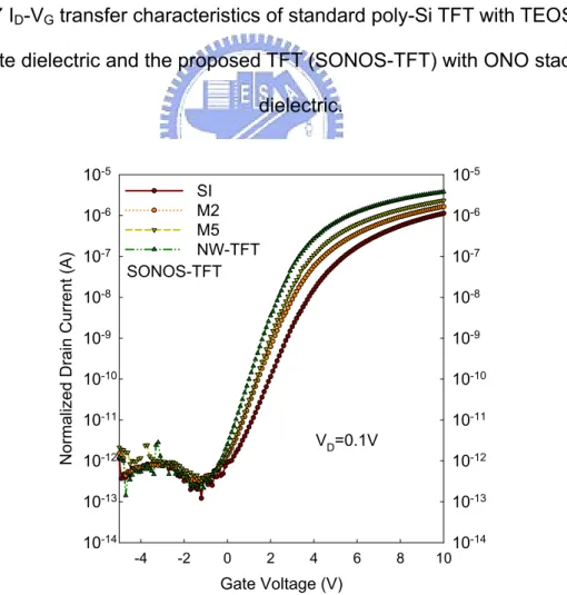
Figure 2-7 shows the typical ID-VG transfer characteristics of standard
poly-Si TFT with TEOS oxide gate dielectric and the proposed TFT (SONOS-TFT) with ONO stack gate dielectric. The standard TFT has the maximum on-current of 7.5 μA, minimum leakage current of 68 pA, and an ON/OFF ratio of 1 × 10⁵. The SONOS-TFT has the maximum on-current
increased from 7.5 μA to 17.4 μA, minimum leakage current decreased from 68 pA to 33 pA, and the current ratio increased from 1 × 10⁵ to 5 × 10⁵. In addition,
the SONOS-TFT. The enhanced performance in electrical characteristics of the SONOS-TFT is mainly attributed to the increase of the effective gate dielectric constant. By calculating the total gate capacitance composed of the parallel multilayer capacitance, the estimated effective gate dielectric constant is 5.1. Furthermore, the accumulation of N at the SiO2/ poly-Si interface atoms and its
bonding with poly-Si of active layer result a lower interface trap density [9].
In this experiment, except the increasing of the effective gate dielectric constant by using ONO multilayer, the TFTs with multiple channels were also proposed to further improve the performance. There were four different structures single-channel (S1), two stripes of multiple 0.5μm channels (M2), five stripes of multiple 0.2μm channels (M5) and ten stripes of multiple 65nm nanowires (NW) fabricated and compared. Figure 2-4 shows the SEM micrograph of the NW SONOS-TFT, including the gate, source, drain and ten multiple nanowire channels. Figure 2-5 shows the TEM micrograph and the physical width of each channel is confirmed 65 nm.
Figure 2-8 presents the transfer ID-VG curves of the proposed all
SONOS-TFTs with various numbers of channels with different widths. Obviously, the NW has the highest drain current, smallest threshold voltage and the most steep sub threshold slope than others TFTs.
Figure 2-9 shows the maximum normalized drain current of the SONOS-TFTs and the standard TFTs versus the different structures at VD = 5V.
The current of the SONOS-TFTs is increased significantly from 1.7 × 10⁻⁵ A to
1.1 × 10⁻⁴ A and the standard TFTs is increased from 7.5 × 10⁻⁶ A to 7.7 × 10⁻⁵ A
in order from the S1 TFT to the NW TFT. The corner effect of the devices is the main reason for the improve resent of the electrical performance. Due to the crowding of gate fringing field at the corner edges, the electrical field at the corner is obviously larger than that at the surface of the channel. The higher carrier density is induced by the lager electrical field and the better gate control ability is also obtained across the corner in previous papers [10]. The corner effect is significant as the channel number increasing and its each channel width decreasing. Therefore, the pronounced enhancement of the NW TFT is attributed the most corner numbers and its corner effect.
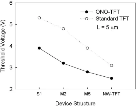
Figure 2-10 shows the threshold voltage (Vth) of the SONOS-TFTs and
standard TFTs versus the multiple channels with different widths. The Vth is
defined as the normalized drain current at 10 nA for VD = 0.1 V. The Vth of the
SONOS-TFT is decreased from 3.9 V to 2.5 V and the standard TFT is decreased from 5.3 V to 3.1 V in order from the S1 TFT to the NW TFT. The improvement of Vth is mainly attributed the corner effect. As reported in [11], it is
indicated that drain current of the corner turns on earlier the surface current of channel. The additional corner current can increase the drain current, thus the Vth was reduced by the constant current definition. In Fig 2-10, the Vth is reduced
with the increasing corner numbers from the S1 TFT to the NW TFT. The NW TFT structure has most corner numbers, the lowest threshold voltage can be obtained both in the SONOS-TFT and the standard TFT.
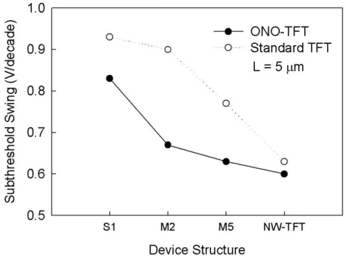
Figure 2-11 shows the subthreshold swing (S.S.) of the SONOS-TFTs and standard TFTs versus the multiple channels with different widths. The S.S. is defined as the amount of gate voltage required to increase drain current by one order of magnitude. The S.S. of the SONOS-TFT is decreased from 0.83 V/decade to 0.6 V/decade and the standard TFT is decreased from 0.93 V/decade to 0.63 V/decade in order from the S1 TFT to the NW TFT. At the sub threshold region, the corner effect can enhance the sub threshold current with additional induced electron density at the corner region [12]. Therefore, the S.S. is reduced with the corner numbers increasing in order from the S1 TFT to the NW TFT. In addition, the current of the corner is also related to its radius, so the device with the smaller radius has the larger corner current. The simulated current of the device at the corner with different radius is reported in [11]. It is found that the sub threshold swing with NW TFT in the SONOS-TFT and the
standard are almost the same, hence the gate control ability is dominated by the corner effect in the NW TFT structure.
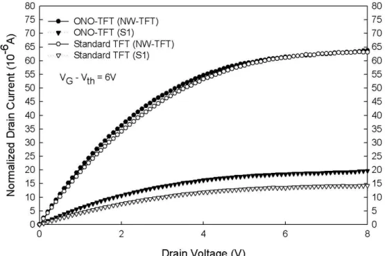
Figure 2-12 show the output ID-VD curves of the SONOS-TFTs versus the
multiple channels with different widths at VGS = 6 V. It is apparent that the
saturation drain current is dramatically increased from the S1 TFT to the NW TFT because of the corner effect. Figure 2-13 shows the output characteristics of the standard TFTs and SONOS-TFT with S1 and NW TFT structures. For S1 TFT, the maximum drain output current of SONOS-TFT is 1.35 times of standard-TFT, consisting with the gate dielectric constant ratio KONO/KSiO2 = 1.31.
However, the current of the NW TFTs is equivalent both in the SONOS-TFTs and standard TFTs without gate dielectric constant ratio KONO/KSiO2 improved effect.
This result reveals that the electrical performance of NW TFTs is dominated by the corner effect.
2-5 Summary
This chapter has proposed a high performance TFT with a nanowire structure and multilayer ONO gate dielectric. The proposed TFT with ONO gate dielectric has the better electrical properties to the standard TFT with TEOS
oxide film. Furthermore, this study applied multiple channels structures to SONOS-TFT and standard TFT to promote device performance. Experimental results indicate that the device performance enhanced with the increasing of number channels, from S1, M2, M5 to NW SONOS-TFTs, because the structure with more corner numbers and shorter radius has the better gate control by the corner effect. Therefore, NW SONOS-TFTs exhibit superior electrical performance, including the high current drivability, low threshold voltage, steep subthreshold slope and favorable output characteristics. The results also reveal that the characteristics of devices with nanowire structure are almost the same comparing the SONOS-TFT and standard TFT, hence devices with nanowire structure are dominated by the corner effect. Such TFTs are thus very promising candidates for use in future high performance poly-Si TFT application.
Fig. 2-1 The schematic plot of SONOS-TFT.
Fig. 2-3 The top view of the NW SONOS-TFT structure
Fig. 2-4 The scanning electron microscopy (SEM) photography of the poly-Si active region of the NW SONOS-TFT.
Fig. 2-5 The transmission electron microscopy (TEM) of the 65nm nanowire channel and the ONO stacked layer in the NW SONOS-TFT.
Fig. 2-6 A schematic MOSFET cross section, showing the axes of coordinates and the bias voltages at the four terminals for the drain-current model.
Fig. 2-7 ID-VG transfer characteristics of standard poly-Si TFT with TEOS oxide
gate dielectric and the proposed TFT (SONOS-TFT) with ONO stack gate dielectric. Gate Voltage (V) -4 -2 0 2 4 6 8 10 Norma lized Dra in Curr ent (A) 10-14 10-13 10-12 10-11 10-10 10-9 10-8 10-7 10-6 10-5 10-14 10-13 10-12 10-11 10-10 10-9 10-8 10-7 10-6 10-5 SI M2 M5 NW-TFT SONOS-TFT VD=0.1V
Fig. 2-8 The transfer ID-VG curves of the proposed all SONOS-TFTs with various
Fig. 2-9 The maximum normalized drain current of the SONOS-TFTs and the standard TFTs versus the different structures at VD = 5V.
Fig. 2-10 The threshold voltage (Vth) of the SONOS-TFTs and standard TFTs
Fig. 2-11 The sub threshold swing (S.S.) of the SONOS-TFTs and standard TFTs versus the multiple channels with different widths.
Fig. 2-12 ID-VD curves of the SONOS-TFTs versus the multiple channels with
Fig. 2-13 ID-VD curves of the standard TFTs and SONOS-TFT with S1 and NW
Chapter 3
SONOS-TFT for Memory Device Application
In this chapter, the memory characteristics for SONOS-TFT, such as program/erase efficiency, retention and endurance, will be discussed. The SONOS-TFT can be used in three dimensional memory structures and the system-on-panel (SOP) applications.
3-1 The Fabrication of SONOS-TFT
The fabrication of the SONOS-TFT with ten strips nanowire channels and a single channel are the same as described in Chapter 2-1.
3-2 The Program/Erase Mechanism
Most novel nonvolatile memories, such as nanocrystal and SONOS memories are based on the concept of Flash memory. If a datum has to be stored in a bit of the memory, there are different procedures. The threshold voltage shift of a Flash transistor can be written as [1]:
FC T C Q V =− Δ (3-1)
between the floating gate (FG) and control gate. The threshold voltage of the memory cell can be altered by changing the amount of charge present between the gate and channel, corresponding to the two states of the memory cell, i.e., the binary values (“1” and “0”) of the stored bit. Figure 3-1 [2] shows the threshold voltage shift between two states in a Flash memory. To a nonvolatile memory, it can be “written” into either state “1” or “0” by either “programming” or “erasing” methods, which are decided by the definition of memory cell itself. There are many solutions to achieve “programming” or “erasing”. In general, hot electron injection (HEI), Fowler-Nordheim tunneling and band to band tunneling are the three kinds of operation mechanisms employed in nonvolatile memories. The three mechanisms will lead to difference characteristics for nonvolatile memories.
3-2-1. Hot-Electron Injection
The physical mechanism of HEI is relatively simple to understand qualitatively. An electron traveling from the source to the drain gains energy from the lateral electric field and loses energy to the lattice vibrations (acoustic and optical phonons). At low fields, this is a dynamic equilibrium condition, which holds until the field strength reaches approximately 100 kV/cm [3]. For fields
exceeding this value, electrons are no longer in equilibrium with the lattice, and their energy relative to the conduction band edge begins to increase. Electrons are “heated” by the high lateral electric field, and a small fraction of them have enough energy to surmount the barrier between oxide and silicon conduction band edges (channel hot electron, CHE). Figure 3-2 [1] shows schematic representation of HEI MOSFET and the energy-distribution function with different electrical fields. On the other hand, the effective mass of hole is heavier than one of electron. It is too hard to obtain enough energy to surmount oxide barrier. Therefore, hot-hole injection is rarely employed in nonvolatile memory operation.
3-2-2. Tunneling Injection
Tunneling mechanisms are demonstrated in quantum mechanics. Basically, tunneling injection must have available states on the other side of the barrier for the carriers to tunnel into. If we assume elastic tunneling, this is a reasonable assumption due to the thin oxide thickness involved. Namely, no energy loss during tunneling processes. Tunneling through the oxide can be attributed to different carrier-injection mechanisms, which process applies depends on the oxide thickness and the applied gate field or voltage. Direct tunneling (DT),
Fowler-Nordheim tunneling (FN), modified Fowler-Nordheim tunneling (MFN) and trap assistant tunneling (TAT) are the main programming mechanisms employed in memory [4-6] as shown in Fig.3-3.
3-3 Retention and Endurance for Nonvolatile Fresh Memory
3-3-1. Retention
In any nonvolatile memory technology, it is essential to retain data for over ten years. This means the loss of charge stored in the storage medium must be as low as possible. For example, in modern Flash cells, FG capacitance is approximately 1 fF. A loss of only 1 fC can cause a 1V threshold voltage shift. If we consider the constraints on data retention in ten years, this means that a loss of less than five electrons per day can be tolerated [1].
Possible causes of charge loss are: 1) by tunneling or thermionic emission mechanisms; 2) defects in the tunnel oxide; and 3) detrapping of charge from insulating layers surrounding the storage medium.
First, several discharge mechanisms may be responsible for time and temperature dependent retention behavior of nonvolatile memory devices. Figure 3-4 shows a bandgap diagram of a SONOS device in the excess electron
state [7], illustrating trap-to-band tunneling, trap-to-trap tunneling, and band-to-trap tunneling, thermal excitation and Poole-Frenkel emission retention loss mechanisms. These mechanisms may be classified into two categories. The first category contains tunneling processes that are not temperature sensitive (trap-to-band tunneling, trap-to-trap tunneling, and band-to-trap tunneling). The second category contains those mechanisms that are temperature dependent. Trapped electrons may redistribute vertically inside the nitride by Poole–Frenkel emission, which will give rise to a shift in the threshold voltage. Moreover, at elevated temperatures, trapped electrons can also be thermally excited out of the nitride traps and into the conduction band of the nitride (thermal excitation), and drift toward the tunnel oxide, followed by a subsequent tunneling to the silicon substrate.
Secondly, the generation of defects in the tunnel oxide can be divided into an extrinsic and an intrinsic one. The former is due to defects in the device structure; the latter to the physical mechanisms that are used to program and erase the cell.
Electrons can be trapped in the insulating layers surrounding the storage medium during wafer processing, as a result of the so-called plasma damage, or even during the UV exposure normally used to bring the cell in a well-defined
state at the end of the process. The electrons can subsequently detrap with time, especially at high temperature. The charge variation results in a variation of the storage medium potential and thus in channel length decrease [8].
The retention capability of Flash memories has to be checked by using accelerated tests that usually adopt screening electric fields and hostile environments at high temperature.
3-3-2. Endurance
Endurance is the number of erase/write operations that the memory will complete and continue to operate as specified in the data sheet. Generally speaking, Flash products are specified for 106 erase/program cycles.
Nevertheless, the endurance requirement may be relaxed with the increase of memory density for the other applications. Figure 3-5 shows the Endurance requirement of NAND Flash memories [9]. The endurance requirement was relaxed to 100K cycles for 256 MB density. In the higher density, a certain cell in a block has less possibility to be written and erased since the memory operation on the cell is repeated after using up the whole memory blocks. The endurance requirement is sufficient for the user to take 700 photos with a 1MB size every day for 10 years [9].
A typical result of an endurance test on a single cell is shown in Fig. 3-6 As the experiment was performed applying constant pulses, the variations of program and erase threshold voltage levels are described as “program/erase threshold voltage window closure” and give a measure of the tunnel oxide aging [8] [10].
In particular, the reduction of the programmed threshold with cycling is due to trap generation in the oxide and to interface state generation at the drain side of the channel. The evolution of the erase threshold voltage reflects the dynamics of net fixed charge in the tunnel oxide as a function of the injected charge. The initial lowering of the erase is due to a pile-up of positive charge which enhances tunneling efficiency, while the long-term increase of the erase is due to a generation of negative traps.
Moreover, a high field stress on thin oxide is known to increase the current density at low electric field. The excess current component, which causes a significant deviation from the current–voltage curves from the theoretical FN characteristics at low field, is known as stress-induced leakage current (SILC). SILC is clearly attributed by stress-induced oxide defects, which leads to a trap assisted tunneling (see Fig. 3-7). The main parameters controlling SILC are the stress field, the amount of charge injected during the stress, and the oxide
thickness. For fixed stress conditions, the leakage current increases strongly with decreasing oxide thickness [11-13].
3-4 The Electrical Characteristics of SONOS-TFT with Multiple
Nanowire Channels.
3-4-1. Program / Erase Characteristics
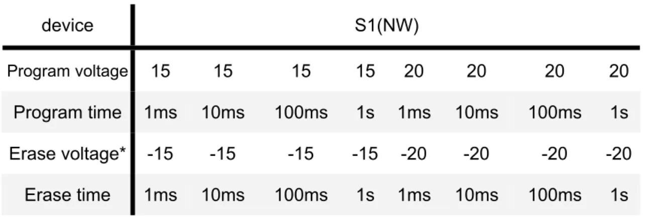
In this study, the devices are programmed and erased by tunneling mechanism, the program and erase conditions for NW SONOS-TFT and S1 SONOS-TFT are listed at Table 3-1. Figure 3-8 (a) and (b) present the transfer ID-VG curves of S1 and NW structures with the various program time at a 15V
program voltage. It is obviously found that the program efficiency of NW SONOS-TFT is better than S1 device. Similarly, the higher program speed is also observed in NW SONOS-TFT comparing S1 SONOS-TFT at a program voltage 20V, as shown in Fig. 3-9 (a) and (b). Figure 3-10 shows the program characteristics of NW and S1 SONOS-TFTs with different gate voltage. At a programming voltage of 15V, the device with nanowire structure can achieve 2.3V Vth shift in 1 ms, which is 1000 times faster than the programming speed
SONOS-TFTs with different gate voltage. At an erasing voltage of -15V, the device with nanowire structure can achieve -0.6V Vth shift in 10 ms, which is
about 100 times faster than the erasing speed with S1 structure.
As mentioned as the Chapter 2-4, the device with multiple nanowire channels structure has the pronounced corner effect comparing the device with a single channel (S1) structure. Since the electrical field at the corner is obviously larger than that at the surface of the channel, the electron injection into the nitride layer at the corner region is easier than surface region. Since the NW SONOS-TFT has more corner numbers, it obtains higher programming and erasing efficiency.
3-4-2. Retention
The retention characteristics of NW SONOS-TFT and S1 SONOS-TFT at 85oC are shown in Fig. 3-12 given a 20V programming voltage for 2s. It is clear
that the memory window loss of NW SONOS-TFT is lower than 0.5V after extrapolating to retention time of 10 years and still kept about 3V. On the other hand, although the Vth shift of S1 SONOS-TFT is larger at the beginning and
also can be kept about 3V after long retention time, the memory window degradation is more serious than NW SONOS-TFT. Therefore, the NW
SONOS-TFT can provide a better reliability for retention.
We notice that S1 device has the larger Vth shift than NW device after
programmed at 85 oC. The program characteristics are contrary to that at room
temperature. As shown in Fig. 3-13, the electrons are injected from channel via tunneling through the tunnel oxide (path 1) in program operation. Some of the injected electrons are captured by the traps (path 2) of the nitride (either deep traps or shallow traps), while the others will inject into the gate (path3). In nitride layer, the thermal excitation electrons may detrap from trapping states and move to blocking oxide by the field-enhanced Poole-Frenkel (P-F) emission. However, at the high temperature, electrons captured in shallow traps can easily detrap and be drawn out in the high electric field (path 4). Only the electrons in the deep traps remain in the nitride trapping layer. Due to the electrical field in NW SONOS-TFT is larger than in S1, the threshold voltage shift is mainly due to electron trapped in deep trap states. Although the electrons trapped in deep states result in the smaller memory window, a superior retention can be obtained.
3-4-3. Endurance
structures with various P/E cycles. Comparing the device with S1 structure, the device with nanowire structure has a more stable endurance characteristic. As shown in Fig. 3-15, the SONOS-TFT with nanowire structure maintains a 3V Vth
window after 106 P/E cycles.
3-5 Summary
The SONOS-TFT with the nanowire structure is proposed and fabricated for memory applications. The NW SONOS-TFT can provide significant improvement in program/erase speed compared with S1 SONOS-TFT. In addition, the retention characteristics reveal that the NW SONOS-TFT has less memory window loss at raised temperature (850C). This is because that most
injected electrons are captured by the deep traps in NW structure. The endurance shows the steady electrical characteristics and the 3V memory window after 106 P/E cycles operation. Hence, the NW SONOS-TFT could
device S1(NW)
Program voltage 15 15 15 15 20 20 20 20
Program time 1ms 10ms 100ms 1s 1ms 10ms 100ms 1s
Erase voltage* -15 -15 -15 -15 -20 -20 -20 -20
Erase time 1ms 10ms 100ms 1s 1ms 10ms 100ms 1s
Before erase, 25V 1ms program is the first.
Table 3-1. The program / erase condition for S1 and NW SONOS-TFT.
Fig. 3-1 I–V curves of an FG device when there is no charge stored in the FG (curve A) and when a negative charge is stored in the FG (curve B).
Fig. 3-2 Schematic cross section of MOSFET. The energy- distribution function at point X1; Y1 is also shown
Φ1 Si Si3N4 Φ2 XOT Φ1 Si Si3N4 Φ2 XOT DT occur when OT OT OT X E X 2 1 1 > > Φ −Φ Φ FN occur when OT OT X E > Φ1 Φ1 Si Si3N4 Φ2 XOT Φ2 Φ1 Si Si3N4 XOT Φt
MFN occur when TAT occur when
N N ox OT OT OT X X E X ⎟ ⎠ ⎞ ⎜ ⎝ ⎛ + Φ − Φ > > Φ − Φ ε ε 2 1 2 1 N N ox OT OT OT X X E X ⎟ ⎠ ⎞ ⎜ ⎝ ⎛ + Φ > > Φ ε ε 3 3 Φ3 =Φ1−Φ2−Φt
Fig. 3-3 Fourth approaches to programming methods, described by Hu and White
Fig. 3-4 Bandgap diagram of a SONOS device in the excess electron state, showing retention loss mechanisms: trap-to-band tunneling (TB), trap-to-trap tunneling (T-T), band-to-trap tunneling (B-T), thermal excitation (TE) and Poole–Frenkel emission (PF)
Fig. 3-6 Threshold voltage window closure as a function of program/erase cycles on a single cell.
Fig. 3-7 Anomalous SILC modeling. The leakage is caused by a cluster of positive charge generated in the oxide during erase.
VG(volt) -4 -2 0 2 4 6 8 10 NID (A) 10-13 10-12 10-11 10-10 10-9 10-8 10-7 STD 15V 1ms Program 15V 10ms Program 15V 100ms Program 15V 1s Program
Fig. 3-8 (a) The transfer ID-VG curves of S1 structures with the different program
time at a 15V program voltage.
VG(volt) -4 -2 0 2 4 6 8 10 NID (A ) 10-13 10-12 10-11 10-10 10-9 10-8 10-7 10-6 STD 15V 1ms Program 15V 10ms Program 15V 100ms Program 15V 1s Program
Fig. 3-8 (b) The transfer ID-VG curves of NW structures with the different program
VG(volt) -4 -2 0 2 4 6 8 10 NID (A ) 10-13 10-12 10-11 10-10 10-9 10-8 10-7 STD 20V 1ms Program 20V 10ms Program 20V 100ms Program 20V 1s Program
Fig. 3-9 (a) The transfer ID-VG curves of S1 structures with the different program
time at a 20V program voltage.
VG(volt) -4 -2 0 2 4 6 8 10 NID (A ) 10-13 10-12 10-11 10-10 10-9 10-8 10-7 10-6 STD 20V 1ms Program 20V 10ms Program 20V 100ms Program 20V 1s Program
Fig. 3-9 (b) The transfer ID-VG curves of NW structures with the different program
Program time(sec)
0.001 0.01 0.1 1 10Memory window (V)
0 1 2 3 4 5 6 7 NW 15V NW 20V S1 15V S1 20VFig. 3-10 The program characteristics of NW and S1 SONOS-TFTs with different gate voltage.
Erase time(sec)
0.001 0.01 0.1 1 10Memory window(volt)
-1.8 -1.6 -1.4 -1.2 -1.0 -0.8 -0.6 -0.4 -0.2 0.0 NW -15V NW -20V S1 -15V S1 -20VFig. 3-11 The erase characteristics of NW and S1 SONOS-TFTs with different gate voltage.
Time(sec)
100 101 102 103 104 105 106 107 108 109Memory window(volt)
2.0 2.5 3.0 3.5 4.0 4.5 5.0 5.5 2.0 2.5 3.0 3.5 4.0 4.5 5.0 5.5 NW SONOS-TFT S1 SONOS-TFT 10 YearsFig. 3-12 Programming voltage is 20V for 2s. It is clear that the memory window loss of NW SONOS-TFT is lower than 0.5V after extrapolating to retention time of 10 years and still kept about 3V.
e (1) (3) (2) (4) e e e e e e e e e e
Fig. 3-13 (1)Electrons injected from channel via tunneling through the tunnel oxide. (2)Some of the injected electrons are captured by the traps of the nitride.(either deep traps or shallow traps) (3)The thermal excitation electrons may detrap from trapping states and move to blocking oxide by the field-enhanced Poole-Frenkel (P-F) emission. (4)At the high temperature, electrons captured in shallow traps can easily detrap and be drawn out in the high electric field.
X10 Endurance in 20V 10ms Program -40V 10ms Erase
V
G(volt)
-4 -2 0 2 4 6 8 10NI
D(A
)
10-13 10-12 10-11 10-10 10-9 10-8 10-7 10-6 10-5 1P 1E 10P 10E 100P 100E 400P 400E 1000P 1000E 3000P 3000EFig. 3-14 (a) present the transfer ID-VG curves of S1 structures with various P/E
V
G(volt)
-6 -4 -2 0 2 4 6 8 10 12NI
D(A)
10-13 10-12 10-11 10-10 10-9 10-8 10-7 10-6 10-5 1P 1E 10P 10E 100P 100E 400P 400E 1000P 1000E 3000P 3000EFig. 3-14 (b) present the transfer ID-VG curves of NW structures with various P/E
Nunber of times
10
010
110
210
310
410
510
610
7Vth(volt)
4
5
6
7
8
Program EraseFig. 3-15 The SONOS-TFT with nanowire structure maintains a 3V Vth window
Chapter 4
Conclusion
In this thesis, we have successfully fabricated poly-Si SONOS-TFTs with various numbers of channels. The SONOS-TFTs can be used for both driving device application and nonvolatile memory application.
For driving device application, the electrical characteristics with various channel numbers and different gate dielectric are compared and discussed in Section 2-4. It is clear that he SONOS-TFT with ONO gate dielectric can provide higher on-current than the standard TFT with oxide gate dielectric. The devices with multiple nanowire channels have lower threshold voltage, steeper subthreshold slope, and superior driving ability. However, the characteristics of devices with nanowire structure are about the same as compared to the SONOS-TFT and standard TFT. Hence devices with nanowire structure are dominated by the corner effect.
For nonvolatile memory application, the memory characteristics of SONOS-TFT with ten strips nanowire (65nm) structure and a single channel (1μ m) structure are compared and discussed in Section 3-4. The results reveal that the program and erase efficiency are greatly improved in the nanowire structure
due to the larger electric field. In addition, excellent retention and endurance characteristics can be obtained. Therefore, the SONOS-TFT with nanowire structure could become a promising technology for next-generation nonvolatile memories.
Because the SONOS-TFTs have the driving capability and nonvolatile memory property at the same time, driving devices and memory devices can be integrated on the same substrate without increasing the fabrication steps. Hence, SONOS-TFTs are promising candidates for the system-on-panel (SOP) applications in the future.
Chapter 1
[1] H. Oshima and S. Morozumi, “Future trends for TFT integrated circuits on glass substrates,” IEDM Tech. Dig., 157, 1989
[2] M. Stewart, R. S. Howell, L. Pires, and M. K. Hatalis, “Polysilicon TFT technology for active matrix OLED displays,” IEEE Trans. Electron Devices, vol. 48, pp. 845-851, 2001
[3] H. Kuriyama et al., “An asymmetric memory cell using a C-TFT for ULSI SRAM,” Symp. On VLSI Tech., p.38, 1992
[4] T. Yamanaka, T. Hashimoto, N. Hasegawa, T. Tanala, N. Hashimoto, A. Shimizu, N. Ohki, K. Ishibashi, K. Sasaki, T. Nishida, T. Mine, E. Takeda, and T. Nagano, “Advanced TFT SRAM cell technology using a phase-shift lithography,” IEEE Trans. Electron Devices, Vol. 42, pp.1305-1313,1995. [5] K. Nakazawa, “Recrystallization of amorphous silicon films deposited by
low-pressure chemical vapor deposition from Si2H6 gas,” J. Appl. Phys, Vol. 69, pp. 1703-1706, 1991
[6] T. J. King and K. C. Saraswat, “Low-temperature fabrication of poly-Si thin-film transistors,” IEEE Electron Device Lett, Vol. 13, pp. 309-311, 1992. [7] H. Kuriyama, S. Kiyama, S. Noguchi, T. Kuahara, S. Ishida, T. Nohda, K.
Sano, H. Iwata, S. Tsuda, and S. Nakano, “High mobility poly-Si TFT by a new excimer laser annealing method for large area electronics,” IEDM Tech. Dig, Vol. 91, pp. 563, 1991.
[8] K. Suzuki, T. Tanaka, Y. Tosaka, H. Horie, and Y. Arimoto, “Scaling theory for double-gate SOI MOSFET's,” IEEE Trans. Electron Devices, vol. 40, pp. 2326-2329, Dec. 1993.