國 立 交 通 大 學
電子工程學系電子研究所
博 士 論 文
系統層級靜電放電測試下之積體電路
暫態觸發閂鎖效應
TRANSIENT-INDUCED LATCHUP IN CMOS
INTEGRATED CIRCUITS UNDER
SYSTEM-LEVEL ESD TEST
研 究 生:許勝福(Sheng-Fu Hsu)
指導教授:柯明道(Ming-Dou Ker)
系統層級靜電放電測試下之積體電路
暫態觸發閂鎖效應
TRANSIENT-INDUCED LATCHUP IN CMOS
INTEGRATED CIRCUITS UNDER
SYSTEM-LEVEL ESD TEST
研 究 生:許勝福
Student: Sheng-Fu Hsu
指導教授:柯明道
Advisor: Ming-Dou Ker
國 立 交 通 大 學
電子工程學系電子研究所
博 士 論 文
A Dissertation
Submitted to
Institute of Electronics
College of Electrical and Computer Engineering
National Chiao Tung University
For the Degree of Doctor of Philosophy
in
Electronic Engineering
June 2006
Hsinchu, Taiwan, Republic of China
推 薦 函
中華民國 九十五年六月事由:推薦電子研究所博士班研究生許勝福提出論文並參加國立交通大學
博士論文口試。
說明:本校電子研究所博士班研究生許勝福已完成電子研究所規定之學科
及論文研究訓練。
有關學科部份,許君已修畢31學分(請查閱學籍資料),通過資格
考試;有關論文研究部份,許君已完成『系統層級靜電放電測試下
之積體電路暫態觸發閂鎖效應』論文初稿,並已有數篇相關之論文
發表或送審,茲列舉如下:
(A) Referred Journal Papers:
[1]. M.-D. Ker and S.-F. Hsu, “Physical mechanism and device simulation on transient-induced latchup in CMOS ICs under system-level ESD test,” IEEE
Trans. Electron Devices, vol. 52, no. 8, pp. 1821–1831, Aug. 2005.
[2]. M.-D. Ker and S.-F. Hsu, “Evaluation on board-level noise filter networks to suppress transient-induced latchup in CMOS ICs under system-level ESD test,” IEEE Trans. Electromagnetic Compatibility, vol. 48, no. 1, pp. 161–171, Feb. 2006.
[3]. M.-D. Ker and S.-F. Hsu, “Component-level measurement for transient-induced latchup in CMOS ICs under system-level ESD considerations,” IEEE Trans. Device and Materials Reliability, in press, 2006.
[4]. S.-F. Hsu and M.-D. Ker, “Transient-induced latchup dependency on power-pin damping frequency and damping factor in CMOS integrated circuits,” revised by IEEE Trans. Electron Devices.
[5]. S.-F. Hsu and M.-D. Ker, “Dependence of device structures on latchup immunity in high-voltage 40-V CMOS process with drain-extended MOSFETs,” submitted to IEEE Trans. Electron Devices.
(B) International Conference Papers:
[1]. M.-D. Ker and S.-F. Hsu, “Transient-induced latchup in CMOS technology: physical mechanism and device simulation,” in IEDM Tech. Dig., 2004, pp. 937–940.
[2]. M.-D. Ker and S.-F. Hsu, “Evaluation on efficient measurement setup for transient-induced latchup with bi-polar trigger,” in Proc. IEEE International
Reliability Physics Symp., 2005, pp. 121–128.
[3]. S.-F. Hsu and M.-D. Ker, “Dependences of damping frequency and damping factor of bi-polar trigger waveforms on transient-induced latchup,” in Proc. EOS/ESD Symp., 2005, pp. 118–125.
[4]. M.-D. Ker and S.-F. Hsu, “Evaluations on board-level noise filter networks to suppress transient-induced latchup under system-level ESD test,” in Proc.
EOS/ESD Symp., 2005, pp. 262–269.
[5]. S.-F. Hsu and M.-D. Ker, “Study of board-level noise filters to prevent transient-induced latchup in CMOS integrated circuits during EMC/ESD test,” in Proc. International Zurich Symp. on Electromagnetic Compatibility, Singapore, 2006, pp. 533–536.
[6]. S.-F. Hsu, M.-D. Ker, G.-L. Lin, and Y.-N. Jou, “Experimental evaluation and device simulation of device structure influences on latchup immunity in high-voltage 40-V CMOS process,” in Proc. IEEE International Reliability
Physics Symp., 2006, pp. 140–144.
總言之,許君已具備國立交通大學電子研究所應有的訓練水準。因此
推薦許君參加國立交通大學電子研究所博士論文口試。
i
-系統層級靜電放電測試下之積體電路
暫態觸發閂鎖效應
研究生:許勝福
指導教授:柯明道 博士
國立交通大學電子工程學系電子研究所
摘要
隨著半導體製程的持續進步,閂鎖效應(Latchup)的可靠度問題更顯的
日趨重要。由於在互補式金氧半場效電晶體製程中無法避免的寄生矽控整
流器(Silicon Controlled Rectifier, SCR),閂鎖效應可藉由正迴授(Positive
Feedback)機制所觸發。一但閂鎖效應被觸發,巨大的電流便會在積體電路
中產生,造成積體電路產品的電路誤動作,甚至可能因過大的電功率(Power)
造成積體電路產品的永久損毀。因此一直以來,積體電路產業便一直致力
於 發 展 各 種 防 止 閂 鎖 效 應 發 生 的 製 程 技 術 , 如 磊 晶 矽 晶 圓 (Epitaxial
Wafer),退化式井區(Retrograde Well),溝槽隔絕(Trench Isolation),以及矽
在絕緣層上成長(Silicon on Insulator, SOI)等技術。
暫態觸發閂鎖效應(Transient-Induced Latchup)是指一種由快速暫態觸
發源所引起的閂鎖效應。目前為止已有數種暫態觸發源被證實會導致暫態
觸發閂鎖效應的發生,包括電源開啟暫態(Power-On Transition),傳輸線反
射(Transmission Line Reflection),電源供應電壓(Power Supply Voltage)的暫
態過電壓突波(Overshoot)及欠電壓突波(Undershoot),以及電纜放電效應
(Cable Discharge Event, CDE)等。這些暫態觸發源已經有各種相對應的實驗
方法來加以驗證積體電路產品對暫態觸發閂鎖效應的防護能力。除了上述
幾 種 暫 態 觸 發 源 外 , 一 種 新 的 暫 態 觸 發 源 — 系 統 層 級 靜 電 放 電 效 應
(System-Level Electrostatic Discharge),也將在本論文被分析證實為另一種
可導致暫態觸發閂鎖效應發生的暫態觸發源。
電子產品為了符合電磁共容(Electromagnetic Compatibility, EMC)法規
之要求規範,系統層級靜電放電測試通常被用來評估電子產品對系統層級
靜電放電效應的耐受能力(Immunity)。然而在進行系統層級靜電放電測試
時,本論文發現系統層級靜電放電所引發的暫態電流將會導致暫態觸發閂
鎖效應發生,造成待測電子產品的功能誤動作或者是永久損毀。然而目前
為止並沒有任何研究文獻探討造成此一暫態觸發閂鎖效應現象的物理形成
機制。因此相關研究對系統或電路設計者而言非常地迫切需要,以期能提
供系統層級靜電放電所引發暫態觸發閂鎖效應的相關知識及解決方法。
有鑒於此,本論文將針對由系統層級靜電放電測試所引發的暫態觸發
閂鎖效應進行研究分析。主要的研究方向包括:(1)了解造成此暫態觸發閂
鎖效應的物理機制,(2)發展相關的元件層級(Component-Level)實驗設置,
(3)評估各種面板層級(Board-Level)雜訊濾波器對抑制暫態觸發閂鎖效應的
效用,以及(4)暫態觸發閂鎖效應相對於積體電路電源腳位上雜訊電壓之阻
尼頻率(Damping Frequency)及阻尼因子(Damping Factor)的關係。除了上述
有關暫態觸發閂鎖效應的研究主題外,由於高電壓(High Voltage, HV)互補
式金氧半場效電晶體製程中的閂鎖效應一直以來受到工業界所重視。因此
本論文也將針對高電壓互補式金氧半場效電晶體製程,研究各種不同的高
壓元件結構對閂鎖效應敏感度的影響。
本論文第二章首先針對造成此暫態觸發閂鎖效應的物理機制加以探討
分析。經由相關的半導體元件模擬(Device Simulation)分析以及實驗量測驗
証,本論文發現系統層級靜電放電將導致一種電壓振幅會隨時間遞減的欠
iii
-阻尼弦式電壓(Underdamped Sinusoidal Voltage)產生於積體電路的電源腳位
上。此欠阻尼弦式電壓亦稱為雙極性觸發電壓(Bipolar Trigger Voltage)。本
論文證實此種欠阻尼弦式電壓乃造成積體電路產生暫態觸發閂鎖效應的主
要暫態觸發源。此種欠阻尼弦式電壓會使儲存於積體電路內的少數載子
(Minority Carrier)快速移動,進一步形成“掃回電流(Sweep-Back Current)"
而引發暫態觸發閂鎖效應。本論文所提出的實驗驗證及元件模擬技巧能提
供實用的研究分析工具,以期能進一步發展出能有效防止暫態觸發閂鎖效
應的電路設計技巧、佈局(Layout)準則、以及半導體製程技術。
由於目前為止沒有相關的元件層級實驗設置用於評估積體電路對系統
層級靜電放電測試所引發暫態觸發閂鎖效應之防護能力,本論文第三章提
出一種能有效評估積體電路對暫態觸發閂鎖效應防護能力的元件層級實驗
設置。此元件層級實驗設置能產生欠阻尼弦式電壓於待測積體電路的電源
供應電壓上,以用來模擬待測積體電路在實際系統層級靜電放電測試下所
遭受到的靜電放電干擾情形。本論文所提出的元件層級實驗設置不但能精
確評估積體電路對暫態觸發閂鎖效應的防護能力,更能進一步避免積體電
路在暫態觸發閂鎖效應發生時所帶來電性過應力(Electric Over Stress, EOS)
損害。
為了能更進一步地提升積體電路對暫態觸發閂鎖效應的防護能力,本
論文第四章評估了不同面板層級雜訊濾波器對抑制暫態觸發閂鎖效應的實
際效用。這些雜訊濾波元件包括電容濾波器、電容-電感濾波器(LC-Like)、
π形濾波器、亞鐵鹽珠(Ferrite Bead)、暫態突波抑制器(Transient Voltage
Suppressor, TVS)、及混合式濾波器等。藉由這些雜訊濾波元件反耦合
(Decouple)或吸收因系統層級靜電放電測試在積體電路電源(地)端造成的
瞬間雜訊,則積體電路對抑制暫態觸發閂鎖效應的防護能力將可有效提
升。所得到的實驗結果可提供印刷電路板(Printed Circuit Board, PCB)設計者
一個有用的參考準則,以期能利用適當的雜訊濾波器來有效提升積體電路
對暫態觸發閂鎖效應的防護能力。
由於在系統層級靜電放電測試下,雙極性觸發電壓已被證實是造成暫
態觸發閂鎖效應的主要雜訊電壓觸發源,因此決定雙極性觸發電壓的二個
重要參數—阻尼頻率及阻尼因子,決定了暫態觸發閂鎖效應對雙極性觸發
電壓的敏感度。本論文第五章利用元件模擬探討暫態觸發閂鎖效應相對於
雙極性觸發電壓之阻尼頻率及阻尼因子的關係。此相關研究成果可應用在
高效能晶片濾波器(On-Chip Filter)設計,以抑制暫態觸發閂鎖效應。也可應
用於發展高效能元件層級暫態觸發閂鎖效應量測裝置,以準確評估待測積
體電路對抑制暫態觸發閂鎖效應的防護能力。
閂鎖效應在高壓互補式金氧半場效電晶體製程中扮演著一個非常重要
的角色。和一般標準積體電路製程不同的是,利用高壓積體電路製程所製
造出來的積體電路,其額定電源供應電壓一般皆高於十伏特(Volt)。在此高
壓積體電路中所寄生的矽控整流器,其維持電壓(holding voltage)一般皆遠
低於其額定電源供應電壓。這意味著閂鎖效應在高壓積體電路中大多是無
法避免的,導致閂鎖效應在高壓積體電路中扮演著一個極關鍵的角色。有
鑒於此,本論文第六章將針對 0.25 微米高壓 40 伏特積體電路製程中的汲
極擴散(Drain-Extended)金氧半場效電晶體,研究各種不同的元件結構及佈
局幾合參數對於閂鎖效應敏感度的相互關係。所得到的相關實際晶片量測
結果可藉由半導體元件模擬進一步地加以分析驗証。利用本論文所提出的
各種實驗測試結構及元件模擬技巧,可進一步評估萃取(Extract)出能適用在
高壓積體電路中的閂鎖效應防護佈局準則。
以上針對由系統層級靜電放電測試所引發的暫態觸發閂鎖效應,以及
高壓積體電路製程中的閂鎖效應特性,本論文所進行的相關研究皆有實際
晶片量測及元件模擬驗証,並有相對應的國際會議及期刊論文發表。
TRANSIENT-INDUCED LATCHUP IN CMOS INTEGRATED
CIRCUITS UNDER SYSTEM-LEVEL ESD TEST
Student: Sheng-Fu Hsu Advisor: Dr. Ming-Dou Ker
Department of Electronics Engineering and Institute of Electronics
National Chiao-Tung University
Abstract
With the continual scaling of CMOS technologies, latchup is an increasingly significant reliability issue in semiconductor technologies. Because of the parasitic silicon controlled rectifier (SCR) in CMOS technologies, latchup can be initiated via a positive regeneration feedback if there is large enough substrate or well current. Once latchup occurs in a powered system, huge current can conduct through a low-impedance path from the power supply to ground nodes. If the resulting high current is not limited, irreversible damages can occur to the CMOS ICs due to the latchup-generated high power. Even though the latchup current is limited to prevent the permanent damage, it is possible that the CMOS ICs will malfunction. For a long time, IC industry has been devoted to develop process solutions for latchup prevention, such as epitaxial layer, retrograde well, trench isolation, and silicon on insulator (SOI).
Transient-induced latchup (TLU) means a latchup event initiated by a fast “transient” triggering mode. Continual scaling of device feature size leads to an increasing susceptibility to TLU of the CMOS ICs. Thus, the TLU reliability issue has attracted more attentions recently than before in CMOS technologies. Several different transient triggering modes have been proven to be able to initiate TLU, such as power-on transition, transmission line reflections, supply voltage overshoots or undershoots, and cable discharge event (CDE). For these transient triggering modes, several corresponding measurement setups have been also
developed to evaluate the TLU immunity of CMOS ICs. In addition to these transient triggering modes, the system-level electrostatic discharge (ESD) event has been proven a new TLU-triggering mode in this dissertation.
For electronic products to satisfy the electromagnetic compatibility (EMC) regulations, system-level ESD test is necessary to evaluate the system-level ESD robustness of electronic products. During the system-level ESD test, the ESD-generated transient current can induce TLU in CMOS ICs within the electronic products, leading to temporary shutdown or permanent damage of the equipment under test (EUT). So far there is no literature to clarify the physical mechanism of TLU under the system-level ESD test. Thus, a clear understanding of TLU physical mechanism is necessary to help system or IC designers to solve TLU issues under the system-level ESD test.
This dissertation focuses on the analysis and characterization of TLU under the system-level ESD test. Several major topics including: (1) clarification of TLU physical mechanism, (2) development of component-level TLU measurement setup, (3) evaluations of board-level noise filters to suppress TLU, (4) and TLU dependency on power-pin damping frequency and damping factor, are discussed in this dissertation. In addition to the TLU topic, latchup is also a very significant reliability issue in a high-voltage (HV) CMOS process. This dissertation also investigates the dependences of the device structure on latchup immunity in a HV 40-V CMOS process with drain-extended MOSFETs (DEMOS).
In chapter 2, the physical mechanism of TLU in CMOS ICs under the system-level ESD test is clearly characterized by device simulation and experimental verification in time domain. For TLU characterization, an underdamped sinusoidal (bipolar) voltage stimulus has been clarified as the realistic TLU-triggering stimulus under the system-level ESD test. The specific “sweep-back” current caused by the minority carriers stored within the parasitic pnpn structure of CMOS ICs has been qualitatively proved to be the major cause of TLU. Through both the understanding of physical mechanism and the proposed simulation/verification methodology on TLU, the safe design/layout rules or circuit techniques in CMOS ICs can be developed against TLU events.
Because no component-level measurement setup has been developed to evaluate the TLU immunity of CMOS ICs under the system-level ESD test, an efficient component-level TLU measurement setup with bipolar trigger is developed in chapter 3. From the experimental and simulation results, TLU measurement setup without a current-blocking diode but with a small current-limiting resistance is suggested to accurately evaluate the TLU immunity of CMOS ICs without over estimation or electric over stress (EOS) damage to DUT.
The proposed component-level TLU measurement setup can be widely utilized to evaluate the TLU immunity of CMOS ICs in practical field applications.
To further suppress the susceptibility to TLU under the system-level ESD test, different board-level noise filter networks are evaluated in chapter 4 to find their effectiveness for TLU prevention under the system-level ESD test. By using the proposed component-level TLU measurement setup in this dissertation, it can be proved that the TLU immunity of CMOS ICs can be greatly improved with proper noise filter networks. All the experimental evaluations have been verified with the SCR test structures and the ring oscillator circuit fabricated in a 0.25-μm CMOS technology.
TLU dependency on two dominant parameters of the TLU-triggering bipolar voltage―damping frequency and damping factor, is also investigated by device simulation and experimental measurement in chapter 5. Damping frequency and damping factor are two dominant parameters of bipolar transient noises, and they are strongly dependent on the system shielding, board-level noise filter, chip-/board- level layout, etc. The simulated TLU characteristics are useful for optimizing a bipolar trigger to evaluate the TLU immunity of CMOS ICs without overestimation. Furthermore, the board-/chip- level noise filters can be properly designed to efficiently eliminate the ESD-coupled noises for TLU prevention.
In order to characterize the latchup characteristics in HV CMOS process, chapter 6 investigates the dependence of device structures on latchup immunity in a 0.25-μm HV 40-V CMOS process with DEMOS transistors. Layout parameters such as anode-to-cathode spacing and guard ring width are also investigated to find their impacts on latchup immunity. All the experimental results can be qualitatively and quantitatively verified with 2-D device simulation. Both the proposed latchup test structures and simulation methodologies can be further applied to extract safe and compact design rule for latchup prevention in HV CMOS ICs.
誌 謝
在此首先要感謝柯明道教授這四年來的細心指導與鼓勵,使我得
以順利完成博士學位。在柯教授的指導教誨下,除了在課業研究上所
獲得的指導外,柯教授認真的研究態度與嚴謹的處事原則更讓我獲益
良多,也讓我了解到如何面對並克服困難的重要性。
在這段求學過程中,我要特別感謝『工研院系統晶片技術發展中
心』的『產品與靜電防護技術部』、『奇景光電股份有限公司』、『世
界先進積體電路股份有限公司』、『閎康科技股份有限公司』等給予
我在研究方面的支持與協助。在此我要特別感謝曾任職於『工研院系
統晶片技術發展中心』的林昆賢博士、莊哲豪先生、陳子平先生,任
職於『奇景光電股份有限公司』的蔡志忠副總、陳東暘博士、羅文裕
先生,任職於『世界先進積體電路股份有限公司』的林耿立經理、周
業甯先生,以及任職於『閎康科技股份有限公司』的謝詠芬博士等人
所給予我在研究方面的支持與協助。
我也要感謝『奈米電子與晶片系統實驗室』的陳世倫、陳榮昇、
徐新智、鄧志剛、張瑋仁、顏承正、蕭淵文、陳世宏以及實驗室其他
學長、同學、及學弟妹們,在我博士班學業生涯中所給予我的支持與
協助。在此也要感謝實驗室助理卓慧貞小姐在實驗室行政事務上的許
多協助。
最後,我要在此由衷感謝我的父親許永賜先生、母親王玉秋女
士、祖父許圳生先生、哥哥許真祿先生、姐姐許雯卿女士、女友陳婉
如小姐,沒有你們這多年來的付出、鼓勵、扶持與照顧,就沒有我今
日的成就,在此再一次表達我最衷心的感謝。另外,要祝福所有在這
幾年來與我相處過的師長、朋友、學弟妹們,有緣與你們同在這一階
段成長,是我一生的榮幸,願大家平安和樂,事事順心!
許 勝 福
謹誌於竹塹交大
九十五年 六月
Contents
Abstract (Chinese)
iAbstract (English)
vAcknowledgements
ixContents
xiTable Captions
xvFigure Captions
xviiChapter 1. Introduction
11.1. Background of Transient-Induced Latchup (TLU) 1
1.2. Categories of TLU-Triggering Modes 2
1.2.1. Power-On Transition 2
1.2.2. Transmission Line Reflections 3 1.2.3. Supply Voltage Overshoots/Undershoots 3
1.2.4. Cable Discharge Event 4
1.2.5. System-Level ESD Event 4
1.3. Organization of This Dissertation 5
Figures 8
Chapter 2. Physical Mechanism and Device Simulation on Transient-
Induced Latchup in CMOS ICs Under System-Level
ESD Test
172.1. Background 17 2.2. TLU under System-Level ESD Test 18 2.3. Test Structure 19 2.4. Measurement Setup 20 2.5. Device Simulation for TLU 21
2.5.1. Simulated Latchup DC I-V Characteristics 22 2.5.2. TLU Simulation with Negative VCharge 22 2.5.3. TLU Simulation with Positive VCharge 24
2.5.4. More Realistic Case 25
2.6.1. Measured Latchup DC I-V Characteristics 26 2.6.2. TLU Measurement with Negative VCharge 26 2.6.3. TLU Measurement with Positive VCharge 26
2.7. Discussion 27
2.7.1. Dominant Parameter to Induce TLU 27 2.7.2. Minimum Applied Voltage Amplitude to Initiate TLU 28 2.7.3. Minimum QStored or ISb to Initiate TLU 28 2.7.4. Transient Responses on the Minority Carriers Stored
within SCR 29
2.8. Conclusion 30
Figures 31
Chapter 3. Component-Level Measurement for Transient-Induced
Latchup in CMOS ICs under System-Level ESD
Considerations
453.1. Background 45 3.2. Component-Level TLU Measurement Setup 46 3.3. Experimental Results 47
3.3.1. Dependences of Current-Blocking Diode and Current-
Limiting Resistance on Bipolar Trigger Waveforms 48
3.3.1.1. Positive VCharge 48
3.3.1.2. Negative VCharge 48
3.3.2. Dependences of Current-Blocking Diode and Current-
Limiting Resistance on TLU Level 49
3.3.2.1. Latchup DC I-V Characteristics of SCR
Structures 49
3.3.2.2. Positive TLU Level 50
3.3.2.3. Negative TLU Level 51
3.4. TLU Simulation 52 3.4.1. Dependences of Current-Blocking Diode on TLU Level 52 3.4.2. Dependences of Current-Limiting Resistance on
TLU Level 53
3.5. Suggested Component-Level TLU Measurement Setup 54 3.6. TLU Verification on Real Circuits 55 3.7. Conclusion 56
Tables 57
Figures 58
Chapter 4. Evaluation on Board-Level Noise Filter Networks to
Suppress Transient-Induced Latchup in CMOS ICs
under System-Level ESD Test
714.1. Background 71 4.2. Dependencies of Board-Level Noise Filters on Bi-Polar Trigger
Waveform under System-Level ESD Test 72
4.3. Measurement Setup 74 4.4. Experimental Evaluation 75
4.4.1. TLU Level of the SCR Structure without Noise
Filter Network 75
4.4.2. TLU Level of the SCR Structure with Noise
Filter Networks 75
4.4.2.1. Capacitor Filter, LC-Like Filter, and
π-Section Filter 75
4.4.2.2. Ferrite Bead, TVS, and Hybrid
Type Filters 77
4.5. Verification on Real Circuits 78
4.5.1. TLU Transient Waveforms of the Ring Oscillator 79 4.5.2. TLU Level of the Ring Oscillator with Noise
Filter Networks 79
4.6. Conclusion 80
Figures 81
Chapter 5. Transient-Induced Latchup Dependency on Power-Pin
Damping Frequency and Damping Factor in CMOS
Integrated Circuits
93Nomenclature 93
5.1. Background 94 5.2. Examples of Different DFreq and DFactor under System-Level
ESD Test 95
5.3. TLU Simulation 96
5.3.1. Relations between DFactor and Minimum Positive
5.3.2. Relations between DFreq and Minimum Positive
(Negative) VP to Initiate TLU 97
5.3.3. Relations between DFactor and Minimum (Maximum)
DFreq to Initiate TLU 98
5.4. Experimental Verification on TLU 99 5.5. Suggested Guidelines for TLU Prevention 101
5.6. Conclusion 102
Figures 103
Chapter 6. Dependence of Device Structures on Latchup Immunity in
High-Voltage 40-V CMOS Process with Drain-Extended
MOSFETs
1136.1. Background 113
6.2. Device Structures of DEMOS Transistors 114
6.2.1. Isolated and Non-Isolated Device Structures 115 6.2.2. Symmetric and Asymmetric Device Structures 115
6.3. HV Latchup Test Structures 116 6.4. Experimental Results 117
6.4.1. Relationships between Latchup Trigger (Holding)
Voltage and Anode-to-Cathode Spacing 118 6.4.2. Relationships between Latchup Trigger (Holding)
Voltage and Guard Ring Width 119
6.5. Device Simulation 120
6.6. Conclusion 121
Tables 122
Figures 123
Chapter 7. Conclusions and Future Works
135
7.1. Specific New Results of This Dissertation 135 7.2. Future Works 136
References
137Vita
143Table Captions
Chapter 3
Table 3.1 TLU levels of the ring oscillators with two sets of layout parameters under four different TLU measurement setups.
Chapter 6
Table 6.1 Summary of the device structures of DEMOS transistors in latchup test structures A, B, and C.
Table 6.2 Summary of the dependence of DEMOS device structures on latchup robustness.
Figure Captions
Chapter 1
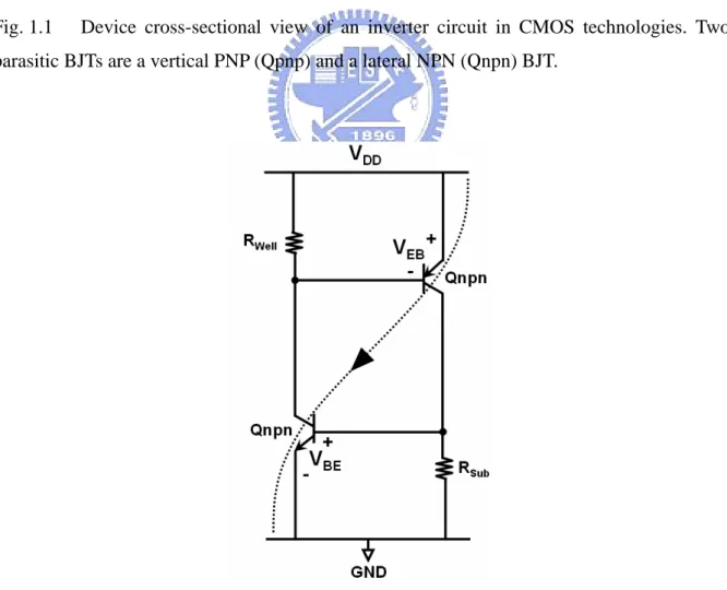
Fig. 1.1 Device cross-sectional view of an inverter circuit in CMOS technologies. Two
parasitic BJTs are a vertical PNP (Qpnp) and a lateral NPN (Qnpn) BJT.
Fig. 1.2 Equivalent circuit of the parasitic SCR in CMOS technologies.
Fig. 1.3 Time-dependent power-supply voltage during the power-on transition.
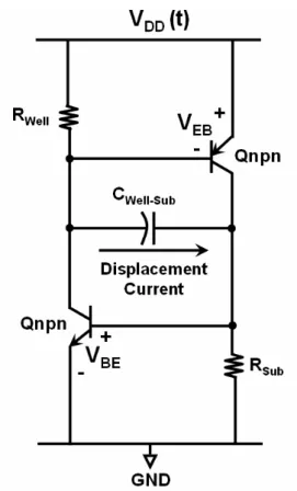
Fig. 1.4 Displacement current generated by the rapid-increasing power-supply voltage on
the well/substrate junction capacitance (CWell-Sub).
Fig. 1.5 Transient voltage overshoots or undershoots on the I/O pins of CMOS ICs due to
the transmission line reflections.
Fig. 1.6 Techniques to simulate the transient (a) overshoots, and (b) undershoots, on the
I/O pins of CMOS ICs.
Fig. 1.7 Transient overshoots or undershoots on the power-supply voltage due to the noise
decoupling under system or environment disturbance.
Fig. 1.8 Techniques to simulate the transient (a) overshoots, and (b) undershoots on
power-supply voltage of CMOS ICs. VDD,n is the nominal circuit operating voltage.
Fig. 1.9 Example of the CDE event occurring on the Ethernet interface of computer
systems.
Fig. 1.10 Example of the system-level ESD test with direct contact discharge on an
electronic product.
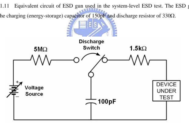
Fig. 1.11 Equivalent circuit of ESD gun used in the system-level ESD test is shown in Fig.
1.11. The ESD gun has the charging (energy-storage) capacitor of 150pF and discharge resistor of 330Ω.
Fig. 1.12 Equivalent circuit of human body model (HBM) in the component-level ESD test.
The charging capacitor (discharge resistor) is a smaller (larger) value of 100pF (1.5kΩ).
Chapter 2
Fig. 2.1 System-level ESD test on a notebook with direct contact-discharge mode
according to IEC 61000-4-2 international standard [32]. The inset figure depicts the typically measured waveforms of transient noise voltage on the power pins of CMOS ICs, which locate within the EUT, under the system-level ESD test [35], [38], [39].
Fig. 2.2 Measurement setup of the system-level ESD test with indirect contact-discharge
test mode [32]. The ESD gun zapping on the horizontal coupling plane (HCP) could cause TLU events on all the CMOS ICs inside the EUT.
Fig. 2.3 For ESD gun with ESD voltage of +1000V zapping on the HCP, the measured VDD transient waveform on one of the CMOS ICs (CMOS IC#A) inside the EUT.
Fig. 2.4 For ESD gun with ESD voltage of +2000V zapping on the HCP, the measured VDD, IDD, and VOUT transient waveforms on CMOS IC#A inside the EUT. TLU
occurs during the system-level ESD test.
Fig. 2.5 (a) Device cross-sectional view, and (b) layout top view, of the SCR structure for
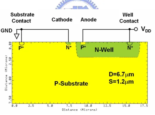
TLU measurements. Geometrical parameters such as D, S, and W represent the distances between well-edge and well (substrate) contact, anode and cathode, and the adjacent well (substrate) contacts, respectively.
Fig. 2.6 The SCR structure used in a two-dimensional device simulation tool (MEDICI).
The specified SCR structure with the geometrical parameters of D=6.7μm and
S=1.2μm is used for all the TLU device simulations in this chapter.
Fig. 2.7 A component-level TLU measurement setup [41], [42]. It can accurately simulate
how an IC inside the EUT will be disturbed by the ESD-generated noise under the system-level ESD test.
Fig. 2.8 Measured VDD waveform for the SCR structure with VCharge of (a) +10V, and (b)
-2V. Clearly, the intended positive-going (negative-going) underdamped sinusoidal voltage can be generated just as that under the system-level ESD test for ESD gun with positive (negative) voltage [35].
Fig. 2.9 Simulated latchup DC I-V characteristic for the SCR structure. Under a latchup
state, the fact that IDD is about 150mA when VDD keeps at its normal operating
voltage (+2.5V) will offer a vital evidence to prove whether TLU certainly occurs in time domain through device simulation.
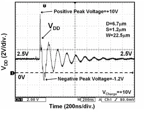
Fig. 2.10 Simulated VDD and IDD transient responses for TLU with a negative VCharge.
During the period of 62.5ns≤t≤87.5ns, the “sweep-back” current, ISb, will be
produced to initiate TLU (IDD significantly increases) when VDD increase from its
negative peak voltage to the normal operating voltage of +2.5V.
Fig. 2.11 Simulated transient responses of both anode current and well contact current for
TLU with a negative VCharge. During the period of 62.5ns≤t≤87.5ns, latctup will be
triggered on by ISb. Meanwhile, huge anode current will conduct through the pnpn
latchup path of the SCR structure.
Fig. 2.12 Simulated 2-D current flow lines with respect to various transient timing points
for TLU with a negative VCharge. Forward well (substrate) contact current appears
when N-well/P-substrate junction is forward-biased (timing points A, B, and F), and TLU will be triggered on due to large enough ISb (timing points C-E, G, and
H).
Fig. 2.13 Simulated VDD and IDD transient responses for TLU with a positive VCharge. During
the period of 50ns≤t≤75ns, TLU will not be triggered on by the N-well/P-substrate junction displacement current. Afterwards, during the period of 87.5ns≤t≤112.5ns, ISb will be produced to initiate TLU (IDD significantly
increases) when VDD increase from its negative peak voltage to the normal
operating voltage, +2.5V.
for TLU with a positive VCharge. The N-well/P-substrate junction displacement
current will not cause TLU (timing points A and B) until large enough ISb is
produced (timing points E-H).
Fig. 2.15 Simulated VDD, GND, and IDD transient responses for TLU under a more realistic
situation. VDD and GND can be disturbed simultaneously by EMI under a
system-level ESD test [35], [38], [39]. Once VDD-to-GND voltage is negative
enough (87.5ns≤t≤100ns) to produce large enough ISb, afterwards TLU could be
easily triggered on when VDD-to-GND voltage returns to a positive voltage
(100ns≤t≤112.5ns).
Fig. 2.16 Measured latchup DC I-V characteristic for the SCR structure.
Fig. 2.17 Measured VDD and IDD transient waveforms from the TLU test with a negative
VCharge of -5V. It is consistent with the device simulation results in Fig. 2.10 that
TLU will be triggered on (IDD significantly increases) when VDD increase from its
negative peak voltage to the normal operating voltage, +2.5V.
Fig. 2.18 Measured VDD and IDD transient waveforms from the TLU test with a positive
VCharge of +20V. It is consistent with the device simulation results in Fig. 2.13 that
TLU will not be initially (VDD>0V) triggered on by the N-well/P-substrate
junction displacement current until large enough ISb is produced when VDD
increases from its negative peak voltage to the normal operating voltage, +2.5V.
Fig. 2.19 Total stored minority carriers, QStored, causing ISb (tA≤t≤tB) inside the N-well region.
The inset figure is an ideal 1-D diode used for deriving the 1-D analytical model of the averaged ISb (≡IAve) [28], [29].
Fig. 2.20 Simulated Va- dependences on damping frequency (f). Va- is defined as the
minimum magnitude of the negative applied voltage to initiate TLU.
Fig. 2.21 Calculated transient responses of QStored (hole) in the N-well region. The
underdamped sinusoidal voltage has the same parameters as those used in the negative VCharge case of Figs. 2.10 and 2.11 (Da, f, and Va of 2×10⁷s-1, 20MHz, and
-14.6V, respectively).
Chapter 3
Fig. 3.1 Component-level TLU measurement setup with bipolar trigger [41], [42], [46]. It
can accurately simulate how a CMOS IC will be disturbed by the ESD-generated noises under system-level ESD test.
Fig. 3.2 For TLU measurement setup with a current-limiting resistance of 5Ω but without
the current-blocking diode, the measured VDD and IDD transient responses with VCharge of (a) -3V, (b) -6V, and (c) +13V.
Fig. 3.3 Measured VDD and IDD transient waveforms with a positive VCharge of +8V. (a) Neither current-blocking diode nor current-limiting resistance, (b) a current-limiting resistance of 20Ω but without a current-blocking diode, and (c) a current-blocking diode (PR1507) but without a current-limiting resistance, is used in the TLU measurement setup.
Neither current-blocking diode nor current-limiting resistance, (b) a current-limiting resistance of 20Ω but without a current-blocking diode, and (c) a current-blocking diode (PR1507) but without a current-limiting resistance, is used in the TLU measurement setup.
Fig. 3.5 Measured latchup DC I-V characteristics of two SCR structures with the same D
(16.6μm) and W (22.5μm) but different S of 1.2μm and 20μm.
Fig. 3.6 Relations between positive TLU level and current-limiting resistances under
different current-blocking diodes. The SCR structure has the layout parameters of (a) D=16.6μm, S=1.2μm, and W=22.5μm, and (b) D=16.6μm, S=20μm, and W=22.5μm.
Fig. 3.7 Measured VDD and IDD transient waveforms with a positive VCharge of +35V. A current-blocking diode (PR1507) and a current-limiting resistance of 20Ω are used in the TLU measurement setup.
Fig. 3.8 Relations between negative TLU level and current-limiting resistances under
different current-blocking diodes. The SCR structure has the layout parameters of (a) D=16.6μm, S=1.2μm, and W=22.5μm, and (b) D=16.6μm, S=20μm, and W=22.5μm.
Fig. 3.9 SCR structure used in a two-dimensional device simulation tool (MEDICI). This
specified SCR structure has the same geometrical parameters (D=16.6μm and
S=1.2μm) of SCR silicon test chips.
Fig. 3.10 Simulated VDD and IDD transient responses for TLU with unipolar trigger. It can simulate the VDD voltage disturbance in Fig. 3.3(c) for TLU measurement setup equipped with the current-blocking diode. TLU cannot be initiated even though VPeak is as high as +20V.
Fig. 3.11 Simulated VDD and IDD transient responses for TLU with bipolar trigger. It can simulate the VDD voltage disturbance in Fig. 3.3(a) for TLU measurement setup without the current-blocking diode. TLU can be initiated even though VPeak is as low as +13V.
Fig. 3.12 Simulated VDD and IDD transient responses for TLU with unipolar trigger. VDD has a VPeak of +25V, which is larger than +20V in Fig. 3.10, so the increasing rate (≡+VPeak-2.5V/rise time) of VDD is large enough to produce large IDs to initiate TLU.
Fig. 3.13 Simulated VDD and IDD transient responses for TLU with bipolar trigger. Compared to Fig. 3.11, it can simulate the bipolar trigger with a larger damping factor in Fig. 3.3(b) for TLU measurement setup equipped with a current-limiting resistance. TLU cannot be initiated due to insufficient ISb.
Fig. 3.14 (a) Schematic diagram, and (b) layout top view, of the ring oscillator. The
geometrical parameters such as X, Y, and Z represent the distances between well-edge and well (substrate) contact, source (drain) regions of PMOS and NMOS, and the adjacent well (substrate) contacts, respectively.
Fig. 3.15 Measured VDD1, IDD1, and VOUT transient waveforms of the ring oscillator with a VCharge of (a) +7V, and (b) -5V. A current-limiting resistance of 5Ω but without a
current-blocking diode is used in the TLU measurement setup.
Chapter 4
Fig. 4.1 Measured VDD transient waveform on one (CMOS IC#1) of the CMOS ICs inside the EUT with ESD voltage of -1000V zapping on the HCP. VDD waveform acts as a bi-polar voltage due to the disturbance of the high ESD-coupled energy.
Fig. 4.2 With an additional decoupling capacitance of (a) 1nF, and (b) 0.1μF, between VDD and VSS (ground) of the CMOS IC#1 under system-level ESD test, the measured VDD transient waveform with ESD voltage of -1000V zapping on the HCP. Compared with the original VDD transient waveform in Fig. 4.1, transient peak voltage of VDD waveform can be suppressed to enhance the TLU immunity of CMOS IC#1.
Fig. 4.3 With a bidirectional-type TVS (part number: P6KE series; breakdown voltages:
±6.8V) between VDD and VSS (ground) of the CMOS IC#1 under system-level ESD test, the measured VDD transient waveform with ESD voltage of -1000V zapping on the HCP. Transient peak voltage on VDD of CMOS IC#1 can be greatly reduced when it exceeds the VBR of TVS.
Fig. 4.4 With a resistor-type ferrite bead (minimum impedance of 80Ω at 25MHz) in
series with the VDD pin of the CMOS IC#1 under system-level ESD test, the measured VDD transient waveform with ESD voltage of -1000V zapping on the HCP. The transient peak voltage (damping factor) of VDD waveform is smaller (larger) than that of the original VDD transient waveform in Fig. 4.1.
Fig. 4.5 Measured VDD and IDD transient waveforms on CMOS IC#1 with ESD voltage of -3000V zapping on the HCP. With a large transient peak voltage of ±60V, TLU is triggered on (IDD is kept at a high current of 80mA) after the ESD-induced disturbance on VDD.
Fig. 4.6 With the decoupling capacitance of 0.1μF between VDD and VSS of the CMOS IC#1, the measured VDD and IDD transient waveforms with the same (-3000V) ESD voltage zapping on the HCP. Compared with the measured waveforms in Fig. 4.5, TLU does not occur, because ESD-induced disturbance on VDD is greatly reduced.
Fig. 4.7 A modified component-level TLU measurement setup with bi-polar trigger [41],
[42]. It can accurately simulate how a CMOS IC inside the EUT will be disturbed by the ESD-generated noises under system-level ESD test.
Fig. 4.8 Without any board-level noise filters, the measured VDD and IDD transient responses of the SCR with VCharge of (a) -2V, and (b) -7V.
Fig. 4.9 With an additional decoupling capacitance of 0.1μF between VDD and VSS (ground) of the SCR, the measured VDD and IDD transient responses with VCharge of -15V. With the help of the decoupling capacitor for suppressing the transient negative peak voltage of VDD down to -0.8V, TLU will not be initiated.
Fig. 4.10 Measured TLU level of the SCR structures with (a) various D and W but a fixed S
are rather susceptible to TLU for all different geometrical parameters (the magnitudes of both positive and negative TLU levels are all smaller than 18V) unless the SCR is latchup-free.
Fig. 4.11 Three types of noise filter networks investigated for their improvements on TLU
level of SCR: (a) capacitor filter, (b) LC-like filter, and (c) π-section filter.
Fig. 4.12 Relations between the decoupling capacitance and the TLU level of the SCR
under three types of noise filter networks: capacitor filter, LC-like filter, and π-section filter.
Fig. 4.13 Four other types of noise filter networks investigated for their improvements on
TLU level of SCR: (a) ferrite bead, (b) TVS, (c) hybrid type I, and (d) hybrid type II.
Fig. 4.14 Relations among the TLU level of SCR, minimum impedance of ferrite bead at
25MHz, and the breakdown voltage of TVS under four types of noise filter networks: ferrite bead, TVS, hybrid type I, and hybrid type II.
Fig. 4.15 Measured VDD1, IDD1, and VOUT transient responses for the ring oscillator (a) without, and (b) with, the board-level noise filter network.
Fig. 4.16 Relations between the decoupling capacitance and the TLU level of the ring
oscillator under three types of noise filter networks: capacitor filter, LC-like filter, and π-section filter.
Fig. 4.17 Relations among the TLU level of the ring oscillator, minimum impedance of
ferrite bead at 25MHz, and the breakdown voltage of TVS under four types of noise filter networks: ferrite bead, TVS, hybrid type I, and hybrid type II.
Chapter 5
Fig. 5.1 With ESD voltage of +1000V zapping on the HCP, the measured VDD transient waveform on one (CMOS IC#1) of the CMOS ICs inside the EUT. VDD waveform is a bipolar voltage due to the disturbance of high ESD-coupled energy.
Fig. 5.2 With an additional decoupling capacitance of 1nF between VDD and VSS (ground) of the CMOS IC#1, the measured VDD transient waveform with ESD voltage of +1000V zapping on the HCP. Compared with the original VDD transient waveform in Fig. 5.1, DFreq, DFactor, and +VPeak are all different.
Fig. 5.3 With a resistor-type ferrite bead (minimum impedance of 80Ω at 25MHz) in
series with the VDD pin of the CMOS IC#1, the measured VDD transient waveform with ESD voltage of +1000V zapping on the HCP. DFactor is larger than that of the original VDD waveform in Fig. 5.1.
Fig. 5.4 Without any board-level noise-decoupling filter on CMOS IC#1, the measured
VDD transient waveform with a higher ESD voltage of +2000V zapping on the HCP. The +VPeak of +30V doubles that (+15V) in Fig. 5.1 with a smaller ESD voltage of +1000V.
Fig. 5.5 Measured VDD and IDD transient waveforms on CMOS IC#1 with ESD voltage of +3000V zapping on the HCP. With a large transient peak voltage of ±50V, TLU is
triggered on (IDD is kept at a high current of 80mA) after the ESD-induced disturbance on VDD.
Fig. 5.6 With the decoupling capacitance of 0.1μF between VDD and VSS of the CMOS IC#1, the measured VDD and IDD transient waveforms with ESD voltage of +3000V zapping on the HCP. TLU does not occur due to different DFreq, DFactor, and +VPeak (-VPeak).
Fig. 5.7 Relations between (a) DFactor and VP+ (VP-), and (b) DFreq and VP+ (VP-). VP+ (VP-) is defined as the magnitude of minimum positive (negative) VP to initiate TLU.
Fig. 5.8 Simulated VDD and IDD transient responses for bipolar trigger voltage with DFactor, DFreq, and VP of 1.5×10⁶s-1, 0.1MHz, and -200V, respectively. TLU doesn’t occur because tP is too long (~3μs) to generate sufficient ISb [28], [29].
Fig. 5.9 Simulated VDD and IDD transient responses for bipolar trigger voltage with the same parameters as those in Fig. 5.8 but with VP of +150V. TLU can be triggered on by IDs while VDD initially increases from the normal operating voltage (+2.5V) to +VPeak.
Fig. 5.10 Simulated VDD and IDD transient responses for bipolar trigger voltage with DFactor, DFreq, and VP of 1.5×10⁶s-1, 2GHz, and -60V, respectively. IDD cannot follow the VDD variation in time for such a high-DFreq (>1GHz) bipolar trigger, because +IPeak doesn’t simultaneously appear with +VPeak but at the end of the first duration (~50.5ns).
Fig. 5.11 Relations between (a) DFactor and DFreq(min), and (b) DFactor and DFreq(max). DFreq(min) (DFreq(max)) is defined as the minimum (maximum) DFreq to initiate TLU under a fixed VP of +15V or -15V.
Fig. 5.12 Measured VDD and IDD transient responses of the SCR with VCharge of (a) +10V, and (b) +14V.
Fig. 5.13 With a discharge resistor with resistance of 1.5kΩ between the relay and the VDD node in TLU measurement setup (Fig. 2.7), the measured VDD and IDD transient responses with VCharge of (a) +120V, and (b) +200V. In Figs. 5.12(b) and 5.13(b), the minimum -VPeak to initiate TLU is fixed (-2.5V) for the same SCR structure (D=6.7μm, S=1.2μm, and W=22.5μm).
Fig. 5.14 Relations between the decoupling capacitance and the TLU level of SCR.
Chapter 6
Fig. 6.1 Device cross-sectional views of the (a) isolated, and (b) non-isolated, n-DEMOS. Fig. 6.2 Device cross-sectional view of the isolated p-DEMOS.
Fig. 6.3 Device cross-sectional view of the non-isolated symmetric n-DEMOS.
Fig. 6.4 Device cross-sectional view of the inverter logic circuit consisting of a
non-isolated asymmetric n-DEMOS and an isolated asymmetric p-DEMOS.
Fig. 6.5 (a) Device cross-sectional view, and (b) layout top view, of the test structure A.
non-isolated asymmetric n-DEMOS and isolated asymmetric p-DEMOS.
Fig. 6.6 (a) Device cross-sectional view, and (b) layout top view, of the test structure B.
Test structure B is used to simulate the parasitic SCR resulting from the non-isolated symmetric n-DEMOS and isolated symmetric p-DEMOS.
Fig. 6.7 (a) Device cross-sectional view, and (b) layout top view, of the test structure C.
Test structure C is used to simulate the parasitic SCR resulting from the isolated asymmetric n-DEMOS and p-DEMOS.
Fig. 6.8 Relationships between TLP-measured latchup trigger (holding) voltage and
anode-to-cathode spacing for test structures A, B, and C.
Fig. 6.9 TLP-measured latchup I-V characteristics of test structure C with anode-to-
cathode spacing of 27.5μm.
Fig. 6.10 TLP-measured latchup I-V characteristics of test structure A with anode-to-
cathode spacing of 31.6μm.
Fig. 6.11 TLP-measured latchup I-V characteristics of test structure B with anode-to-
cathode spacing of 31.6μm.
Fig. 6.12 Relationships between TLP-measured latchup trigger (holding) voltage and guard
ring width for test structures A, B, and C with anode-to-cathode spacing (parameter “X”) of 19.6μm, 25.6μm, and 27.5μm, respectively.
Fig. 6.13 Device structures used in the 2-D device simulation for (a) test structure A, (b)
test structure B, and (c) test structure C. These device structures have the same layout parameters as the silicon test chips.
Fig. 6.14 Simulated latchup I-V characteristics for the test structures A and B with
anode-to-cathode spacing of 31.6μm, and for the test structure C with anode-to-cathode spacing of 27.5μm. All these test structures have the same guard ring width of 0.8μm.
Fig. 6.15 Simulated 2-D current flow lines under latchup condition for (a) test structure A,
Chapter 1
Introduction
In this chapter, the background and the organization of this dissertation are discussed. First, the background of transient-induced latchup (TLU) is introduced. Secondly, the categories of TLU-triggering modes in field applications are discussed. Finally, the organization of this dissertation is well described.
1.1. Background of Transient-Induced Latchup (TLU)
It has been a long time since latchup was a significant reliability issue in semiconductor technologies [1]-[15]. Latchup originates from the parasitic silicon controlled rectifier (SCR), which is composed of two cross-coupled parasitic bipolar junction transistors (BJTs) in CMOS technologies. The device cross-sectional view of an inverter circuit is shown in Fig. 1.1. These two parasitic BJTs are a vertical PNP (Qpnp) and a lateral NPN (Qnpn) BJT. The equivalent circuit of the parasitic SCR is illustrated in Fig. 1.2. Once there is large enough substrate (well) current flowing through the parasitic substrate (well) resistance of RSub (RWell), the Qnpn (Qpnp) will be turned on because of its forward-biased emitter-base junction. Thus, the other Qpnp (Qnpn) will be also turned on via the mechanism of the positive regeneration feedback. If the product of the beta gains of these two BJTs is larger than one, this positive feedback mechanism can lead to a large current conducting through a low-impedance path from VDD (source of PMOS) to GND (source of NMOS). This phenomenon is the so called latchup. As a result, CMOS ICs will malfunction or even be burned out due to the latchup-generated high power.
TLU means a latchup event initiated by a fast “transient” triggering mode. Once some transient triggering mode happens to generate large enough substrate or well current in CMOS ICs, TLU can be triggered on via a positive-feedback mechanism. With the continual scaling of CMOS technologies [16], the smaller device feature size enables a larger packing density of transistors in CMOS chips. However, CMOS ICs are more susceptible to TLU because the spacing from N+ to P+ junction has been also continuously decreasing. Thus, the
reliability issue of TLU has attracted more attentions recently than before in CMOS technologies [17]-[25]. For the quasi-static latchup, the formal test standard [26] has been announced and widely used for evaluations of latchup immunity. For TLU, however, there is no related formal test standard, but only “standard practice” [27] to evaluate the TLU immunity of CMOS ICs. Thus, it’s necessary to clarify the TLU physical mechanism, to develop an efficient TLU measurement setup, and to develop a useful TLU-protection design for high-robustness CMOS ICs.
1.2. Categories of TLU-Triggering Modes
Several different transient triggering modes have been proven to be able to initiate TLU [3]-[6], [20], [21], [27]. These transient triggering modes include power-on transition [3], [4], transmission line reflections [5], [6], supply voltage overshoots [20] or undershoots [27], and cable discharge event (CDE) [21]. In most of these transient triggering modes, their corresponding measurement setups have been also developed to evaluate the TLU immunity of CMOS ICs. In addition to these transient triggering modes, a new TLU-triggering mode called system-level electrostatic discharge (ESD) event [28], [29] has been analyzed in this dissertation. These TLU-triggering modes are introduced below.
1.2.1. Power-On Transition [3], [4]
When power-supply voltage ramps up from 0V to its normal circuit operating voltage during the power-on transition, the displacement current will be formed due to the rapid-increasing power-supply voltage. The time-dependent power-supply voltage during the power-on transition is shown in Fig. 1.3. The ramp rate (RA) of the power-supply voltage during the power-on transition can be expressed as
DD r V RA T ≡ . (1.1) VDD is the normal circuit operating voltage, and Tr is the rise time of power-supply voltage. Once RA is above some critical value, TLU will be triggered on by the large enough displacement current that flows through the well/substrate junction capacitance (CWell-Sub) of CMOS ICs, as shown in Fig. 1.4. By applying different ramp rates of the power-supply voltage, the threshold ramp rate to initiate TLU can be evaluated. The susceptibility of this TLU is strongly dependent on the ramp rate of the power-supply voltage, because TLU can occur even if the normal circuit operating voltage is far below the required latchup trigger
voltage in DC latchup I-V characteristic.
1.2.2. Transmission Line Reflections [5], [6]
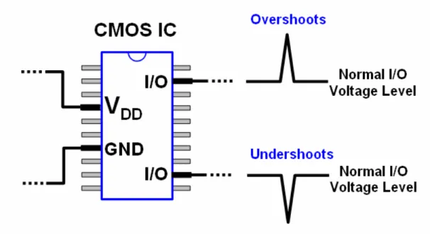
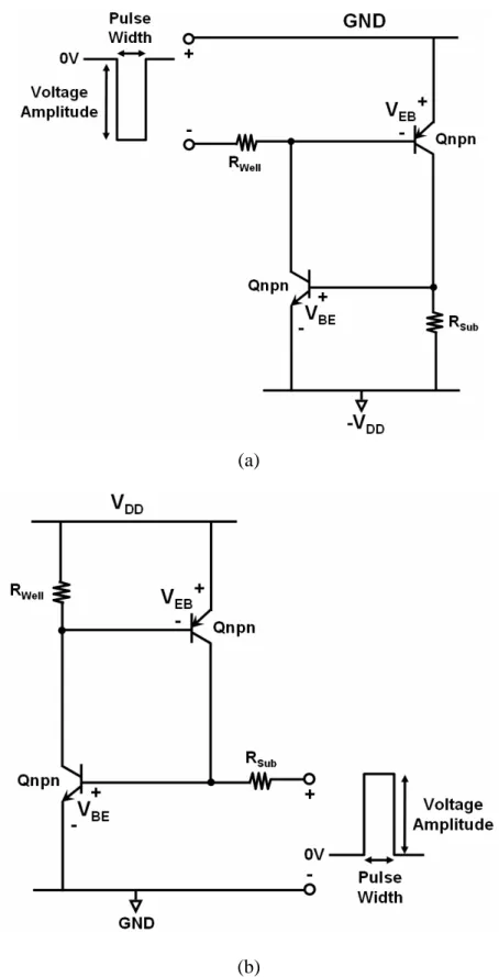
When the transmission line reflections take place due to impedance mismatch during signal propagation, transient voltage overshoots or undershoots can occur on the I/O pins of CMOS ICs, as shown in Fig. 1.5. Because the I/O pins are directly connected to P+ (N+) diffusions in N-well (P-substrate), such transient voltage overshoots (undershoots) can make the emitter-base junction of the parasitic PNP (NPN) BJT momentarily forward-biased. Once the forward-biased emitter-base junction of one parasitic BJT provides enough diffusion current to turn on the other parasitic BJT, the positive-feedback regeneration mechanism can induce TLU. The techniques to simulate transient voltage overshoots and undershoots on the I/O pins of CMOS ICs are shown in Fig. 1.6(a) and 1.6(b), respectively. The transient voltage overshoots (undershoots) can be simulated by applying a rectangular voltage pulse on the emitter-base junction of parasitic PNP (NPN) BJT in CMOS ICs. Thus, the threshold voltage amplitude and pulse width to initiate TLU can be determined. In general, when the pulse width decreases, the threshold voltage amplitude required to induce TLU will increase. However, when the pulse width is long enough, a quasi-static situation could be reached. As a result, the threshold voltage amplitude required to induce TLU is approximate to the DC bias (~0.7V) required to turn on the emitter-base junction of the parasitic BJT in CMOS ICs.
1.2.3. Supply
Voltage
Overshoots/Undershoots [20], [27]
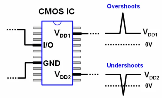
The transient overshoots or undershoots on power-supply voltage can take place due to the noise coupling under system or environment disturbance, as shown in Fig. 1.7. Such transient overshoots or undershoots on power-supply voltage can induce the junction diffusion or displacement current within the CMOS ICs. If the diffusion or displacement current is large enough to activate the parasitic PNP or NPN BJT, TLU can be triggered on and sustained via the regeneration feedback. The techniques to simulate the transient overshoots and undershoots on power-supply voltage are shown in Fig. 1.8(a) and 1.8(b), respectively. The power-supply voltage overshoots (undershoots) can be simulated by applying a positive (negative) rectangular pulse voltage which is superposed on the normal circuit operating voltage (VDD). The positive rectangular pulse voltage can simulate a rapid-increasing power supply voltage, leading to the excitation of transient displacement current. The negative rectangular pulse voltage can simulate a power-supply voltage undershoot with a negative peak voltage, leading to the excitation of P-substrate/N-well
junction diffusion current. Related experimental results show that the threshold voltage amplitude required to initiate TLU will decrease with the pulse width, regardless of positive or negative voltage pulse.
1.2.4.
Cable Discharge Event [21]
Large number of charges can accumulate in cables when the un-terminated cables are dragged on the floor (known as triboelectricity). CDE is the phenomenon in which the accumulated charges in cables are discharged into another object in proximity. An example of the CDE event occurring on the Ethernet interface of computer systems is shown in Fig. 1.9. Once the accumulated static charges in cables are discharged into the I/O pins of the CMOS ICs, TLU can be easily initiated within the CMOS ICs due to the injection of the transient positive or negative current.
CDE-induced TLU is a typical off-chip signal latchup-triggering event, the injection of the CDE-induced current can induce TLU on I/O or internal circuits of CMOS ICs. For the general off-chip signal latchup-triggering events, most CMOS IC products use the EIA/JESD78 latchup test [26] to evaluate the product robustness. Compared with the other off-chip signal latchup-triggering events, however, CDE-induced latchup is a more severe latchup condition because the injection of CDE-induced current can possess peak current of several amperes. Thus, the EIA/JESD78 latchup test standard is unsuitable for evaluations of the CDE-induced latchup robustness, and so far there is no established component-level test standard for CDE-induced latchup. In the state-of-the-art CMOS technologies where the TLU issues are more severe, design methodologies to suppress CDE-induced TLU are necessarily developed.
1.2.5.
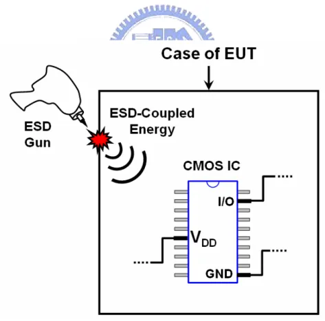
System-Level ESD Event [28], [29]
ESD is a phenomenon due to the electrostatic charges transferring from one object to another with different electric potentials [30], [31]. Usually, huge transient current or electromagnetic interferences (EMI) accompany ESD phenomenon. In real world, electronic products or systems could malfunction or be damaged when subject to ESD events. Thus, system-level ESD event is an important interference source to evaluate the electromagnetic sustainability (EMS) of electronic products. Thus, for electronic products to satisfy the electromagnetic compatibility (EMC) regulations, system-level ESD test [32] is necessary to evaluate the system-level ESD robustness of electronic products.
electronic product is shown in Fig. 1.10. Compared with the component-level ESD tests [33], [34] where the objects under test are ICs, the system-level ESD test aims to evaluate the robustness of electronic products. The equivalent circuit of ESD gun used in the system-level ESD test is shown in Fig. 1.11. The ESD gun has the charging (energy-storage) capacitor of 150pF and discharge resistor of 330Ω. The equivalent circuit of human body model (HBM) in the component-level ESD test is shown in Fig. 1.12. In the HBM component-level ESD test, however, the charging capacitor (discharge resistor) is a smaller (larger) value of 100pF (1.5kΩ). Thus, compared with the ESD current in component-level ESD test, ESD current in system-level ESD test has much larger peak current and shorter rise time, leading to more severe damages for electronic products or their interior ICs. Additionally, ESD protection designs for system- and component- level ESD tests are quite different. It has been proven [35] that a robust CMOS IC product with high component-level ESD levels could be very susceptible to the system-level ESD test. Thus, efficient ESD protection methodologies against system-level ESD events are very significant for electronic products.
During the system-level ESD test, the ESD-generated transient current can induce TLU in CMOS ICs within the electronic products, leading to temporary shutdown or permanent damage of the equipment under test (EUT). However, so far there is no literature to clarify the physical mechanism of TLU under the system-level ESD test. Additionally, no component-level measurement setup has been developed to evaluate the TLU immunity of CMOS ICs under the system-level ESD test. Thus, a clear understanding of TLU physical mechanism is necessary to help system or IC designers to solve TLU issues under the system-level ESD test.
1.3. Organization of This Dissertation
This dissertation is composed of seven chapters. This dissertation (chapter 2 ~ chapter 5) focuses on the analysis and characterization of TLU under the system-level ESD test. Several major topics including: (1) clarification of TLU physical mechanism (chapter 2), (2) development of component-level TLU measurement setup (chapter 3), (3) evaluations of board-level noise filters to suppress TLU (chapter 4), (4) and TLU dependency on power-pin damping frequency and damping factor (chapter 5), are discussed in this dissertation. In addition to the TLU topic, latchup is a very significant reliability issue in a high-voltage (HV) CMOS process [36], [37]. Thus, this dissertation (chapter 6) also investigates the dependences of the device structures on latchup immunity in a HV 40-V CMOS process with
drain-extended MOSFETs (DEMOS). Chapter 7 gives the conclusions and future works of this dissertation. The outlines of each chapter are summarized below.
In chapter 2, the physical mechanism of TLU in CMOS ICs under the system-level ESD test is clearly characterized by device simulation and experimental verification in time domain. For TLU characterization, an underdamped sinusoidal (bipolar) voltage stimulus has been clarified as the realistic TLU-triggering stimulus under the system-level ESD test. The specific “sweep-back” current caused by the minority carriers stored within the parasitic pnpn structure of CMOS ICs has been qualitatively proved to be the major cause of TLU. All the simulation results on TLU have been practically verified in silicon with test chips fabricated in a 0.25-μm CMOS process.
Chapter 3 optimizes an efficient component-level TLU measurement setup with bipolar (underdamped sinusoidal) trigger. The developed measurement setup can accurately evaluate the immunity of CMOS ICs against TLU under the system-level ESD test. Current-blocking diode and current-limiting resistance, which are generally suggested to be used in TLU measurement setup with bipolar trigger, are investigated for their impacts to both bipolar trigger waveforms and TLU immunity of device under test (DUT). All the experimental results have been successfully verified with device simulation. From the experimental and simulation results, TLU measurement setup without a current-blocking diode but with a small current-limiting resistance is suggested, which can accurately evaluate the TLU immunity of CMOS ICs without over estimation or EOS damage to DUT. The suggested measurement setup has been verified with the SCR test structures and the real circuitry (ring oscillator) fabricated in a 0.25-μm CMOS technology.
In chapter 4, different types of board-level noise filter networks are evaluated to find their effectiveness for improving the immunity of CMOS ICs against TLU under the system-level ESD test. By choosing proper components in each noise filter network, the TLU immunity of CMOS ICs can be greatly improved. All the experimental evaluations have been verified with the SCR test structures and the ring oscillator circuit fabricated in a 0.25-μm CMOS technology. Some of such board-level solutions can be further integrated into the chip design to effectively improve the TLU immunity of CMOS IC products.
In chapter 5, TLU dependency on power-pin damping frequency and damping factor is characterized by device simulation and verified by experimental measurement. Damping frequency and damping factor are two dominant parameters of bipolar transient noises, and they are strongly dependent on the system shielding, board-level noise filter, chip-/board-
level layout, etc. From the simulation results, bipolar trigger waveform with damping frequency of several tens of megahertz can trigger on TLU most easily. However, TLU is less sensitive to bipolar trigger waveform with an excessively large damping factor, an excessively high damping frequency, or an excessively low damping frequency. The simulation results have been experimentally verified with the SCR test structures fabricated in a 0.25-μm CMOS technology.
In chapter 6, the dependence of device structures on latchup immunity in a 0.25-μm HV 40-V CMOS process with DEMOS transistors has been verified with silicon test chips and investigated with device simulation. Layout parameters such as anode-to-cathode spacing and guard ring width are also investigated to find their impacts on latchup immunity. It was demonstrated that the drain-extended NMOS (n-DEMOS) with a specific isolated device structure can greatly enhance the latchup immunity. The proposed test structures and simulation methodologies can be applied to extract safe and compact design rule for latchup prevention of DEMOS transistors in HV CMOS process.
Chapter 7 summarizes the main results of this dissertation. Some suggestions for the future works are also addressed in this chapter.
Fig. 1.1 Device cross-sectional view of an inverter circuit in CMOS technologies. Two parasitic BJTs are a vertical PNP (Qpnp) and a lateral NPN (Qnpn) BJT.
Fig. 1.3 Time-dependent power-supply voltage during the power-on transition.
Fig. 1.4 Displacement current generated by the rapid-increasing power-supply voltage on the well/substrate junction capacitance (CWell-Sub).
Fig. 1.5 Transient voltage overshoots or undershoots on the I/O pins of CMOS ICs due to the transmission line reflections.
(a)
(b)
Fig. 1.6 Techniques to simulate the transient (a) overshoots, and (b) undershoots, on the I/O pins of CMOS ICs.
Fig. 1.7 Transient overshoots or undershoots on the power-supply voltage due to the noise coupling under system or environment disturbance.
(a)
(b)
Fig. 1.8 Techniques to simulate the transient (a) overshoots, and (b) undershoots on power-supply voltage of CMOS ICs. VDD is the normal circuit operating voltage.
Fig. 1.9 Example of the CDE event occurring on the Ethernet interface of computer systems.
Fig. 1.10 Example of the system-level ESD test with direct contact discharge test mode on an electronic product.
Fig. 1.11 Equivalent circuit of ESD gun used in the system-level ESD test. The ESD gun has the charging (energy-storage) capacitor of 150pF and discharge resistor of 330Ω.
Fig. 1.12 Equivalent circuit of human body model (HBM) in the component-level ESD test. The charging capacitor (discharge resistor) is a smaller (larger) value of 100pF (1.5kΩ).
![Fig. 2.1 System-level ESD test on a notebook with direct contact-discharge mode according to IEC 61000-4-2 international standard [32]](https://thumb-ap.123doks.com/thumbv2/9libinfo/8634804.192719/59.892.248.647.106.408/level-notebook-direct-contact-discharge-according-international-standard.webp)