Control and improvement of crystalline cracking from GaN thin films
grown on Si by metalorganic chemical vapor deposition
J.W. Yu
a, H.C. Lin
a, Z.C. Feng
a,*, L.S. Wang
b, S. Tripathy
b, S.J. Chua
b aGraduate Institute of Electro-Optical Engineering and Department of Electrical Engineering, National Taiwan University, Taipei 106-17, Taiwan, ROC b
Institute of Materials Research and Engineering, 3 Research Link, 117602 Singapore, Singapore Available online 24 August 2005
Abstract
A series of GaN thin films were grown on Si substrate under different conditions using metalorganic chemical vapor deposition (MOCVD) and characterized by Nomarski microscopy (NM), optical reflectance (OR), high-resolution X-ray diffraction (HRXRD), Raman scattering (RS) and photoluminescence (PL). NM showed different patterns for GaN/Si grown under different growth and source flow parameters. XRD, RS and PL measurements confirmed their wurtzite crystalline GaN structures, and the corresponding line shape analyses revealed their difference corresponding to the NM observations. The control and improvement of the crystalline cracking in GaN/Si are discussed.
D 2005 Elsevier B.V. All rights reserved.
Keywords: GaN; Si; MOCVD; Optical reflectance; X-ray diffraction; Raman scattering; Photoluminescence
1. Introduction
Research and development on GaN-based materials and structures have been greatly enhanced in recent years and remarkable breakthroughs have been achieved in their growth and applications in visible – UV light emitting diode (LED), laser diode (LD) and other optoelectronics/electronic devices. [1 – 5]. Metalorganic chemical vapor deposition (MOCVD) is currently a major technique for the industry mass production of these materials and device wafers with sapphire as the main substrate. SiC is the secondary commonly used material as substrate. However, the insulat-ing nature of sapphire and high costs of SiC have limited their further wider use. Various other substrate materials have been explored. Silicon is an attractive one among them because of its high crystal quality, large area size, low manufacturing cost and the potential application in inte-grated devices. GaN and related materials/structures grown on Si are promising for developing new generation of
devices by combining Si and III-N based materials and technologies in the 21st century.
Due to a large lattice mismatch (17%) and a big difference in thermal expansion coefficients (37%) between GaN and Si [6], which are both larger than that between GaN and sapphire, it is even more difficult to grow high-quality GaN films and structures on Si substrates than on sapphire. In order to realize good quality of GaN films grown on Si, buffer layers with composite structure have been inserted and grown between the GaN epilayer and Si substrate, such as AlN[7], carbonized silicon[8], nitridized GaAs [9], oxidized AlAs [10], g-Al2O3 [11], and
inter-mediate superlattice [12,13]. Recently, to grow GaN on Si(111), Kim et al. [6]used a five-step graded AlxGa1 xN
(x = 0.87 – 0.07) interlayer between AlN buffer layer and GaN epilayer, and Dadgar et al.[14]employed a method to reduce tensile stress and improve GaN layer quality in the early stage of buffer layer growth by an in situ masking of the AlN seed layer with a thin SiN mask. Lee et al. [15]
reported the high-quality GaN by MOCVD using a SixNy
inserting layer between the 1.5 Am GaN overlying layer and the 1.0 Am underlying layer, which was grown on Si(111) with a high-temperature AlN buffer.
0040-6090/$ - see front matterD 2005 Elsevier B.V. All rights reserved. doi:10.1016/j.tsf.2005.07.081
* Corresponding author. Tel.: +886 2 3366 3543; fax: +886 2 2363 7467. E-mail address: [email protected] (Z.C. Feng).
In this paper, we report the growth and characterization for a series of GaN thin films on Si under different conditions by metalorganic chemical vapor deposition (MOCVD). They were characterized by Normarski micro-scopy (NM), optical reflectance (OR), high-resolution X-ray diffraction (HRXRD), Raman scattering (RS) and photoluminescence (PL). The control and improvement of cracks in GaN/Si have been realized by MOCVD growth.
2. Experimental details
GaN epitaxial layers were grown on n-type Si(111) substrates by low pressure (LP) MOCVD in a vertical reactor with a high speed rotation disk holder for multiple wafers. Trimethylgallium (TMGa), trimethylaluminum (TMAI) and high purity ammonia (NH3) were used as
Ga, Al and N precursors, respectively. After a chemical cleaning process, the Si(111) substrate was heated to 1030 -C under hydrogen ambient for 10 min to produce a clean, oxide-free surface. To prevent the melt back etching of Si substrate by TMGa subsequently injected, the high-temper-ature AlN layer was first deposited at 1050 -C. For the samples NS1295, NS1296, NS 1347, the AlN layer is 50 nm thick without Si-doping while in the samples NS 1691 and NS 1692, the AlN layer is 100 nm thick with Si-doping. Finally, the temperature was adjusted to 1000 -C and about 1 – 2 Am thick unintentionally doped GaN epitaxy layer was grown. For samples NS1691 and NS1692, the Si-delta doping was also performed during the GaN growth. More details of growth will be published elsewhere.
After the growth, a series of material characterization techniques, including Nomarski microscopy (NM), X-ray diffraction (XRD), optical reflectance (OR), Raman scat-tering (RS) and photoluminescence (PL) spectroscopy, were used to assess the GaN films. XRD was measured using a Philips X’pert five-crystal diffractometer with a Cu Ka radiation (1.54 A˚ ). OR was measured using a UV – Visible FilmMeter, F20UV. RS was performed by a J-Y microscope under the excitation of 633 nm from a HeNe laser. PL was measured with a Renishaw UV-2000 microscope with the He – Cd laser 325 nm line for excitation. All measurements were performed at room temperature (RT).
3. Results and discussion
Some data summary from characterization are listed in
Table 1for the five experimental GaN/Si samples. Detailed
description can be seen from the following sections. 3.1. Normaski microscopy
Fig. 1 shows the Normaski microscopy photos of five
MOCVD-grown GaN/Si. All graphs are recorded under a magnification of 500 and with an inserted ruler length of 0.2 mm. The variation of cracks with samples grown under different conditions is clearly revealed. Many groups have reported the appearance of cracks along the {1-100} in the GaN layers grown on the Si substrate[6,15 – 17]. Cracks in GaN on Si are known to be formed during the cooling stage due to a large tensile stress caused by the large difference in thermal expansion coefficients [6]. Our present work has shown the variation of cracks with the growth conditions, and the control and optimization of the cracking patterns. The reduction of cracks in some samples (NS1691, NS1692) is caused by the Si-delta doping process. They correspond to the features revealed from structural and optical measurements.
3.2. Film thickness
The film thicknesses were measured by optical reflec-tance (OR). Fig. 2shows such an example for the sample NS1347. The arrow in the left side of the figure indicates the band gap of the epitaxial GaN film, which is close to 360 nm. The simulation on the OR spectrum in the wavelength range of 400 – 850 nm gives the film thickness of d = 778 nm, and also the values of refraction index, n, and the extinct coefficient, k, vary with wavelength.
3.3. High-resolution X-ray diffraction
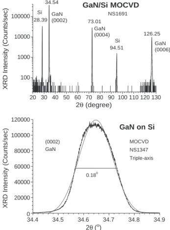
All films were characterized by high-resolution X-ray diffraction (HR-XRD). A typical 2h – x wide scan (20 – 130-) for a GaN/Si sample, NS1691, is shown inFig. 3. It exhibited only the dominant wurtzite (w-) GaN crystalline (0002), (0004) and (0006) peaks plus two peaks from Si substrate. This indicates the grown GaN layer with the normal orientation along the c-axis of wurtzite crystalline structure[18]. The narrow value of 0.18- of the full width at
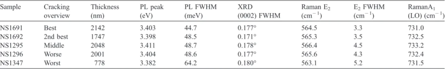
Table 1
Characterization summary for MOCVD-grown GaN/Si samples Sample Cracking overview Thickness (nm) PL peak (eV) PL FWHM (meV) XRD (0002) FWHM Raman E2 (cm 1) E2FWHM (cm 1) RamanA1 (LO) (cm 1) NS1691 Best 2142 3.403 44.7 0.177- 564.5 3.3 731.0 NS1692 2nd best 1747 3.398 48.5 0.171- 565.3 3.5 732.5 NS1295 Middle 2048 3.411 48.7 0.178- 566.4 4.5 733.2 NS1296 Worse 2001 3.404 48.6 0.177- 565.6 4.3 732.4 NS1347 Worst 778 3.382 64.2 0.180- 563.1 5.2 731.5
half maximum (HWFM) on the (0002) GaN peak, as shown in the bottom plot of the figure, indicates the high degree of crystalline perfection of the grown sample. FWHM values
0.0 0.1 0.2 0.3 0.4 0.5 E g MOCVD NS1347 Reflectivity Wavelength (nm) experiment calculation GaN/ Si 2.30 2.35 2.40 2.45 2.50 400 500 600 700 800 400 300 500 600 700 800 0.000 0.005 0.010 0.015 0.020 Wavelength (nm) n k
Fig. 2. The optical reflectance spectrum for a GaN/Si sample, NS1347, measured in 250 – 850 nm (solid line) with simulated data in 400 – 850 nm (dash line). The deduced values of the refraction index, n, and the extinct coefficient, k, are plotted in the bottom side graph.
Fig. 1. Normaski microscopy pattern of five MOCVD-grown GaN/Si. All graphs are with a magnification of 500 and an inserted ruler length of 200 Am.
20 30 40 50 60 70 80 90 100 110 120 130 100 1000 10000 100000 NS1691 GaN/Si MOCVD 126.25 94.51 Si GaN (0006) GaN (0004) 73.01 GaN (0002) 34.54 Si 28.39 XRD Intensity (Counts/sec) 2θ (degree) 34.4 34.5 34.6 34.7 34.8 34.9 0 20000 40000 60000 80000 100000 120000 (0002) GaN 0.18o GaN on Si MOCVD NS1347 Triple-axis XRD Intensity (Counts/sec) 2θ (o)
Fig. 3. The HR-XRD wide (20 – 130-) 2h – x scan for a GaN/Si sample, NS1691 (top graph), and a typical GaN (0002) peak/Gaussian fit for a GaN/ Si, NS1347 (bottom graph).
of the GaN (0002) peak for other samples are also listed in
Table 1. It can be seen that other samples even show even
smaller FWHM values than NS1347, indicating better crystalline quality.
3.4. RT photoluminescence
Fig. 4 shows the RT PL spectra for a GaN/Si sample,
NS1291, with the insert for the expanse of the main peak area. It shows a strong PL emission band at 3.403 eV due to the near band edge emission from wurtzite GaN. It possesses a small FWHM value of 44.7 meV, also indicating a high quality of w-GaN material. The PL peak and FWHM values for five experimental samples are all listed inTable 1. 3.5. Raman scattering
Fig. 5exhibits the RT Raman spectra of five
MOCVD-grown GaN films on Si, and a reference Si (111) bare substrate. Fig. 6 is a typical Raman spectrum with two inserts for the w-GaN characteristic E2and A1(LO) modes [19]as well as their curve fits. The peak frequencies and the
FWHM values of the E2mode for all samples are listed in
Table 1.
4. Conclusions
In this study we have employed MOCVD to grow a series of GaN thin films on Si under different conditions and films were characterized by a variety of techniques. Nomarski microscopy showed different cracking patterns for GaN/Si depending on growth and source flow param-eters. Film thicknesses were determined from optical reflectance. High-resolution XRD, Raman scattering and photoluminescence measurements confirmed their wurtzite crystalline GaN structures, and the corresponding line shape analyses revealed their difference corresponding to the NM observations. It was found that NS1691 has the best shape of widest cracking distribution, the narrowest PL and Raman band, NS 1692 takes the 2nd position while NS1295 is the 3rd one with poor surface morphology. NS1296 and NS1347 have the high density of cracks. The high-temperature AlN buffer growth with Si-doping and the Si-delta doping during the GaN layer growth are useful to realize the control and improvement of cracking in GaN/Si.
Acknowledgement
We acknowledge the help and support from Profs. I. Ferguson, A. Dollitle and C.C. Yang. The work at National Taiwan University was supported by funds from National Science Council of Republic of China, NSC 93-2218-E-002-011 and 93-2215-E-002-035.
References
[1] S. Nakamura, S. Pearton, G. Fasol, The Blue Laser Diode—The Complete Story, Springer, Berlin, 2000.
2.6 2.8 3.0 3.2 3.4 3.6 0 20000 40000 60000 3. 3 0 3. 35 3 .40 3. 45 3. 50 PL Intensity (a.u.) Energy (eV) NS1691 3 .347 44.7 me V 3.403 eV NS1691
Fig. 4. The RT PL spectra for a GaN/Si, NS1691, with the insert for expansion. 500 550 600 650 700 750 (f) Si(100) (e) NS1347 (d) NS1296 (c) NS1295 (b) NS1692 (a) NS1691 A1(LO) E 2 633 nm, 300 K MOCVD GaN on Si Raman Intensity Raman Shift (cm-1)
Fig. 5. Raman spectra of five MOCVD-grown GaN films on Si, and a Si (111) bare substrate, measured under 633 nm from a He – Ne laser at RT.
550 600 650 700 750 0 200 400 600 800 720 730 740 750 0 50 100 150 200 550 560 570 580 0 200 400 600 800 Raman Intensity Raman Shift (cm-1) 633 nm 300 K A1(LO) 732. 5 E2 NS1692 GaN/Si MOCVD 565.3
Fig. 6. A typical Raman spectrum for a MOCVD GaN/Si, with details and Gaussian curve fits shown in two inserts for the E2and A1(LO) modes.
[2] J.I. Pankove, T.D. Moustakas (Eds.), Gallium Nitride (GaN) I, Semiconductors and Semimetals, vol. 50, Academic, San Diego, 1998. [3] H. Morkoc, Nitride Semiconductors and Devices, Springer, Berlin,
1999.
[4] E.T. Yu, M.O. Manasreh (Eds.), III – V Nitride Semiconductors: Applications and Devices, vol. 16 in M.O. Manasreh (Ed.), Optoelec-tronic Properties of Semiconductors and Superlattices (New York, Taylor & Francis, 2003).
[5] M.O. Manasreh, I.T. Ferguson (Eds.), III – V Nitride Semiconductors: Growth, vol. 19 in M.O. Manasreh (Ed.), Optoelectronic Properties of Semiconductors and Superlattices (New York, Taylor & Francis, 2003).
[6] M.-H. Kim, Y.-G. Do, H.C. Kang, D.Y. Noh, S.-J. Park, Appl. Phys. Lett. 79 (2001) 2713.
[7] J. Wan, R. Venugopal, M.R. Melloch, H.W. Liaw, W.J. Rummel, Appl. Phys. Lett. 79 (2001) 1459.
[8] A.J. Steckl, J. Devrajan, C. Tran, R.A. Stall, Appl. Phys. Lett. 69 (1996) 2264.
[9] J.W. Yang, C.J. Sun, Q. Chen, M.Z. Anwar, M.A. Khan, S.A. Nikishin, G.A. Seryogin, A.V. Qsinsky, L. Chernyak, H. Temkin, C. Hu, S. Mahajan, Appl. Phys. Lett. 69 (1996) 3566.
[10] N.P. Kobayashi, J.T. Kobayashi, P.D. Dapkus, W.J. Choi, A.E. Bond, X. Zhang, D.H. Rich, Appl. Phys. Lett. 71 (1997) 3569.
[11] L. Wang, X. Liu, Y. Zan, J. Wang, D. Wang, D. Lu, Z. Wang, Appl. Phys. Lett. 72 (1998) 109.
[12] X. Zhang, S.J. Chua, P. Li, K.B. Chong, Z.C. Feng, Appl. Phys. Lett. 74 (1999) 1984.
[13] X. Zhang, Y.T. Hou, Z.C. Feng, J. Chen, J. Appl. Phys. 88 (2001) 6165.
[14] A. Dadgar, M. Poschenrieder, A. Reiher, J. Blasing, J. Christen, A. Krtschil, T. Finger, T. Hemper, A. Diez, A. Krost, Appl. Phys. Lett. 82 (2003) 28.
[15] K.J. Lee, E.H. Shin, K.Y. Lim, Appl. Phys. Lett. 85 (2004) 1502. [16] C.A. Tran, A. Osinski, R.F. Karlicek Jr., I. Berisher, Appl. Phys. Lett.
75 (1999) 1494.
[17] S. Zamir, B. Meyler, J. Salzman, J. Cryst. Growth 230 (2001) 341. [18] Z.C. Feng, X. Zhang, S.J. Chua, T.R. Yang, J.C. Deng, G. Xu, Thin
Solid Films 409 (2001) 15.