國 立 交 通 大 學
電子工程學系電子研究所
博 士 論 文
類比電路中之n型金氧半導體場效電晶體元件汲極
電流低頻雜訊之探討
Investigation of Drain Current Flicker Noise
in Analog n-MOSFETs
研 究 生:吳俊威
指導教授:汪大暉 博士
類比電路中之 n 型金氧半導體場效電晶體元件
汲極電流低頻雜訊之探討
Investigation of Drain Current Flicker Noise
in Analog n-MOSFETs
研 究 生:吳俊威 Student:Jun-Wei Wu
指導教授:汪大暉 博士 Advisor:Dr. Tahui Wang
國 立 交 通 大 學
電 子 工 程 學 系 電 子 研 究 所 博 士 班
博 士 論 文
A Dissertation
Submitted to Institute of Electronics
College of Electrical Engineering and Computer Science
National Chiao Tung University
in Partial Fulfillment of the Requirements
for the Degree of
Doctor of Philosophy
in
Electronics Engineering
November 2004
類比電路中之 n 型金氧半導體場效電晶體元件
汲極電流低頻雜訊之探討
研究生: 吳俊威
指導教授: 汪大暉博士
國立交通大學
電子工程學系
電子研究所
摘要
CMOS 元件技術具有較低成本、高製程整合度、以及低功率的優
點;但在類比電路的應用中,卻有一主要缺點,及其汲極電流低頻雜
訊過大。為了將金氧半導體場效電晶體成功的運用在類比電路中,元
件設計者必須徹底了解低頻雜訊的物理來源。
首先,吾人將先針對金氧半導體場效電晶體元件中汲極電流低頻
雜訊的熱載子效應作徹底研究。吾人發現,因熱載子效應的影響,在
元件氧化層中會行成局部的氧化層電核累積,此種不均勻的氧化層電
核分布,將會造成通道臨界電壓分布的不均勻,此即為造成雜訊衰減
的主要原因。除此之外,吾人也提供一簡單之兩區域模型使讀者更加
了解我們所提的現象。
接下來,吾人將探討在 0.13µm CMOS 製程中,pocket implantation
製程對於金氧半導體場效電晶體汲極電流低頻雜訊之影響。吾人研究
結果顯示,pocket implantation 製程將會嚴重的衰減低頻雜訊特性,
其原因如下,因為 pocket implantation 的影響,在元件通道中的臨界
電壓之分布已為不均勻。吾人同時提供一兩區域低頻雜訊模型來描述
此 pocket implantation 對於元件低頻雜訊的影響。在我們提供的模型
中,所有參數均由元件量測資料中萃取出來,無任何可隨意調整之參
數。此外,根據此模型模擬之結果與量測資料非常吻合。基於相同的
理論基礎,吾人可以利用元件低頻雜訊的量測,萃取特殊 ONO 記憶
體元件介電層中之載子儲存分布,此分布之資料為記憶體電路設計之
重要資訊。
再者,吾人同時使用 2-D 元件模擬軟體 (MEDICI) 來驗證不均
勻的元件通道臨界電壓分布對於元件低頻雜訊之影響。吾人在模擬
時,利用改變基底電壓與 pocket doping profile,來驗證通道載子分布
不均勻時,對低頻雜訊之影響,其結果與吾人所提之兩區域低頻雜訊
模型預測結果相同。
最後,吾人探討在超薄氧化層 (15Å) 金氧半導體場效電晶體元件
中低頻雜訊的物理來源。根據研究結果,吾人提出一種由 valence band
tunneling 所導致之低頻雜訊來源。在 strong inversion 的情形下,valence
band 中的電子將穿透超薄氧化層,並在 valence band 中留下電洞,如
此 一 來 , 造 成 電 子 電 洞 的 不 平 衡 , 並 導 致 電 子 與 電 洞 的 quasi
Fermi-level 分開。所以,在超薄氧化層元件中之低頻雜訊來源為電子
與 電 洞 在
interface traps
中
recombination
所 產 生 之
generation/recombination 雜訊。我們同時分析 time-domain 中的雜訊,
即所謂 random telegraph signal,其結果與我們所提出之低頻雜訊來源
相符合。
Investigation of Drain Current Flicker Noise
in Analog n-MOSFETs
Student:
Jun-Wei
Wu
Advisor:
Dr.
Tahui
Wang
Institute of Electronics, National Chiao-Tung University
Hsin-Chu, Taiwan, R.O.C.
Abstract
CMOS technology is superior in its low cost, high integration, and low power; nevertheless, there is a major drawback in analog applications. The MOSFETs are so noisy although so called “analog low noise” fabrication process is used. Apart from white thermal noise, MOSFETs are notorious for flicker noise in the low frequency range. So as to improve the MOS circuit’s dynamic range and get better circuit performance, a device designer has to understand the physical origin of flicker noise.
First of all, the hot carrier degradation mechanisms of drain current flicker noise in analog n-MOSFETs are investigated. From our observation, the non-uniform threshold voltage distribution generated by local oxide charges after stressing could give rise to series flicker noise degradation. A simple two-region flicker noise model can be used to give better understanding of this behavior.
Next, pocket implantation effect on drain current flicker noise in 0.13µm CMOS process based high performance analog n-MOSFETs is investigated. Our result shows that pocket implantation will significantly degrade device low-frequency noise primarily because of non-uniform threshold voltage distribution along the channel. An analytical two-region flicker noise model to account for a pocket doping effect is proposed. In our model, the local
threshold voltage and the width of the pocket implant region are extracted from measured reverse short channel effect and the oxide trap density is extracted from a long-channel device. Good agreement between our model and measurement result is obtained without other fitting parameters. In addition, non-uniform threshold voltage distribution along the channel resulting from CHE programming in special ONO charge storage cells would increase drain current flicker noise. Based on the same concept of two-region model, one can extract programming charge distribution in NROM memory devices from noise measurement.
Then, we use a two-dimensional device simulator, MEDICI, to simulate the effect of channel carrier distribution variation on flicker noise. The substrate bias and pocket doping profile is changed to verify the relation between channel carrier distribution and drain current flicker noise. The results show good agreement with the analytical model prediction.
Finally, low frequency flicker noise in analog n-MOSFETs with 15Å gate oxide is investigated. A new noise generation mechanism resulting from valence band electron tunneling is proposed. In strong inversion condition, valence-band electron tunneling from Si substrate to poly-gate takes place and results in the splitting of electron and hole quasi Fermi-levels in the channel. The excess low frequency noise is attributed to electron and hole recombination at interface traps between the two quasi Fermi-levels. Random telegraph signal due to capture of channel electrons and holes is characterized in a small area device to support our model.
致謝
首先,這本博士論文的完成,必須歸功於我的指導老師汪大暉教
授。汪教授對於研究的熱誠與敏感度讓我深深佩服;其深厚的學識基
礎與嚴謹的研究態度,對我的人生觀影響極為深遠。
在論文的研究上必須感謝許多曾經指導過我的學長們
,及一起參
與研究的同學及學弟。首先感謝蔣汝平、鄒年凱、葉致鍇、黃立元、
韓承憲學長在我剛進研究生活的指導與鼓勵;感謝陳奇祥、易成名、
及陳尚志學長在研究領域上的協助及討論
。同時,我也感謝陳旻政、
蔡慶威、王哲麒、張育造同學在我研究路程的大力協助,及鄭念祖、
張鴻智、邱凱翎、李兆琪、鄭志昌、游建文、馬煥淇學弟妹在實驗執
行上的幫助,以及同實驗室之古紹泓,詹前泰學弟的友情支持;感謝
前瞻元件與技術實驗室歷年來同學與學弟的友誼,讓我的研究生活趣
味十足。另外,感謝華邦電子黃智睦、趙傳珍部經理,以及旺宏電子
盧道政副處長及張耀文經理提供我研究上相關的協助及意見。再者,
也感謝國家奈米實驗室組長黃國威博士在實驗儀器上的建議與協
助。對於本系王聖智、蔡中、郭治群教授給予的鼓勵與教誨,也致上
我最深的謝意。最後,感謝我的大學好友們陪我度過漫長的博士班生
涯。
其次,感謝我的父母、外婆、哥哥、大嫂、弟弟、女友郭昱暄小
姐及其家人,在我漫長的求學期間給我的鼓勵與支持,有他們在背後
無怨無悔的付出與關心,讓我毫無顧忌的專注於論文研究,使得這本
博士論文得以順利完成。
另外,我要特別感謝武陵高中數理資優班的許桂淋老師、陳明鈁
老師及簡大漳老師,沒有他們不計代價的悉心指導及教誨,我不可能
在數理方面及未來研究上都有紮實的基礎。
在此,謹將這份榮耀獻給養育我的父母、指導我的汪大暉教授及
已逝世的恩師許桂淋老師。
Contents
Chinese Abstract
iEnglish Abstract
iiiAcknowledgements
vContents
viFigure Captions
ixTable Captions
xviList of Symbols
xviiChapter 1
Introduction
1Chapter 2
Hot Carrier Effect on Drain Current Flicker Noise in
Analog n-MOSFETs
52.1 Introduction 5
2.2 Basic Theory of Flicker Noise 6 2.3 Device Information and Experimental Setup 10 2.4 Flicker Noise Degradation under Different Stress Condition in
Analog n-MOSFETs 10
2.4.1 Maximum Substrate Current Stress 11
2.4.2 Maximum Gate Current Stress 11
2.4.3 Fower-Nordheim Stress 12
2.5 Flicker Noise Degradation under Different Stress Condition in
Special ONO Charge Storage Cells 12
2.5.1 Fower-Nordheim Programming 12
2.5.2 Maximum Gate Current Programming 13
2.6 Two-Region Model of Noise Degradation 13
Chapter 3
Pocket Implantation Effect on Drain Current Flicker
Noise in Analog n-MOSFETs
283.1 Introduction 28
3.2 Device Information 29
3.3 Modeling of Pocket Implantation Effect on Flicker Noise 30 3.3.1 Noise Behavior for Different Pocket Dose 30 3.3.2 Verified by Charge Pumping Method 31 3.3.3 Three-Region Model of Pocket Implant Effect on
Flicker Noise 32
3.4 Application of Three-Region Model in Special ONO Charge
Storage Cell 34
3.4.1 Noise Behavior after Program and Erase 34 3.4.2 Extraction of Programming Charge Distribution
through Noise Measurement 35
3.5 Summary 36
Chapter 4
Influence of Inversion Carrier Distribution on Drain
Current Flicker Noise
554.1 Introduction 55
4.2 Simulation of Channel Carrier Distribution with Different
Pocket Condition 55
4.3 Simulation of Pocket Implantation Effect on Flicker Noise 56 4.4 Substrate Bias Effect on Flicker Noise 58 4.4.1 Measurement Results of Substrate Bias Effect 58 4.4.2 Simulation Results of Substrate Bias Effect 59
4.5 Summary 60
5.1 Introduction 80
5.2 Basic Theory of RTS 81
5.3 Device Information 81
5.4 Results and Discussion 82
5.4.1 Abnormal Noise Characteristics in Frequency Domain 82 5.4.2 Analysis of RTS Behavior in Time Domain 84 5.4.3 Valence-Band Tunneling Induced Noise 84
5.5 Summary 86
Chapter 6
Conclusions
103References
105Vita
113Figure Captions
Chapter 2
Fig. 2-1 The block diagram of noise measurement system.
Fig. 2-2 NMOS (W/L=10µm/0.34µm, tox=65Å) Id-Vg characteristics (measured @ Vd=0.1V) before and after maximum Ib stress (stress bias : Vg=1.64V, Vd=3V).
Fig. 2-3 NMOS (W/L=10µm/0.34µm, tox=65Å) noise characteristics (measured @ Vg=1V, Vd=0.1V) before and after maximum Ib stress (stress bias: Vg=1.64V, Vd=3V).
Fig. 2-4 NMOS (W/L=10µm/0.34µm, tox=65Å) Id-Vg characteristics (measured @ Vd=0.1V) before and after maximum Ig stress (stress bias: Vg=4.7V, Vd=4.7V).
Fig. 2-5 NMOS (W/L=10µm/0.34µm, tox=65Å) noise characteristics (measured @ Vg=1V, Vd=0.1V) before and after maximum Ig stress (stress bias: Vg=4.7V, Vd=4.7V).
Fig. 2-6 NMOS (W/L=10µm/0.34µm, tox=65Å) Id-Vg characteristics (measured @ Vd=0.1V) before and after FN stress (stress bias: Vg=8V, others 0V).
Fig. 2-7 NMOS (W/L=10µm/0.34µm, tox=65Å) noise characteristics (measured @ Vg=1V, Vd=0.1V) before and after FN stress (stress bias: Vg=8V, others 0V).
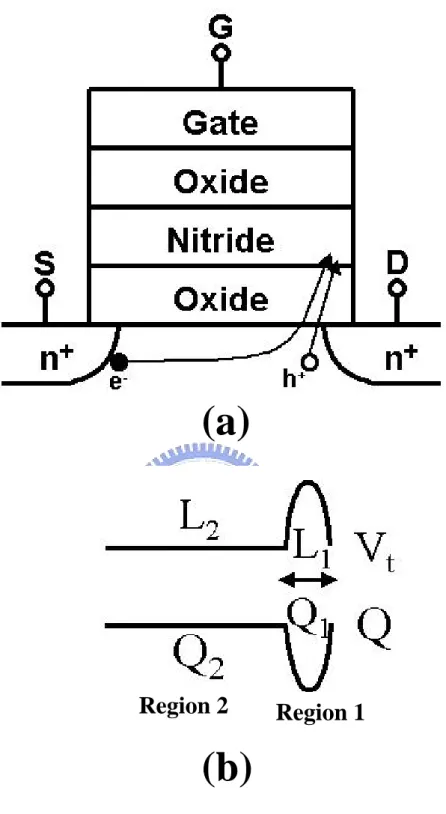
Fig. 2-8 (a) The diagram of special ONO charge storage cell. (b) The oxide charge and threshold voltage distribution along the channel after hot carrier programming.
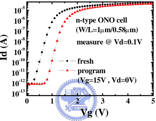
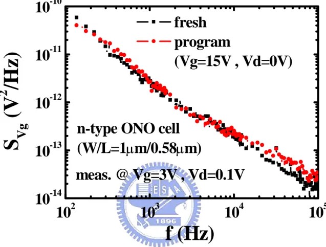
Fig. 2-10 The ONO cell (W/L=1µm/0.58µm) noise characteristics (measured @ Vg=3V, Vd=0.1V) in erase state and FN program state (program bias: Vg=15V).
Fig. 2-11 The ONO cell (W/L=1µm/0.58µm) Id-Vg characteristics (measured @ Vd=0.1V) in fresh state, hot carrier program state (program bias: Vd=4V, Vg=6.5V) and erase state (erase bias: Vd=7V, Vg=-3V).
Fig. 2-12 The ONO cell (W/L=1µm/0.58µm) noise characteristics (measured @ Vg=3V, Vd=0.1V) in fresh state, hot carrier program state (program bias: Vd=4V, Vg=6.5V) and erase state (erase bias: Vd=7V, Vg=-3V).
Chapter 3
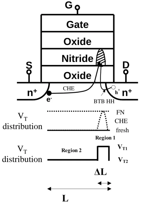
Fig. 3-1 The diagram of pocket implant induced non-uniform threshold voltage distribution along the channel. Region 1 and 3 is the
pocket-implant-affected region and possesses a higher threshold voltage. Region 2 is the rest of the channel.
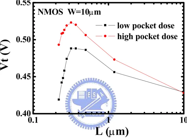
Fig. 3-2 Reverse short channel effect of n-MOSFETs (W=10µm) for low/high pocket doses.
Fig. 3-3 Long channel length NMOS (W/L=10µm/10µm) normalized noise power spectrum density versus gate overdrive voltage (Vg-Vt) for low/high pocket doses. The noise is measured in the linear regime, and all data points are averaged from 3 devices.
Fig. 3-4 Short channel length NMOS (W/L=10µm/0.32µm) normalized noise power spectrum density versus gate overdrive voltage (Vg-Vt) for low/high pocket doses. The noise is measured in the linear regime, and all data points are averaged from 10 devices.
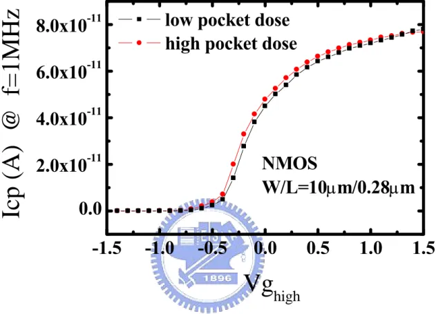
pocket doses. The noise is measured at the same gate overdrive voltage. Fig. 3-6 Charge pumping current versus the high level of gate pulse (Vghigh) in CP
measurement for low/high pocket doses.
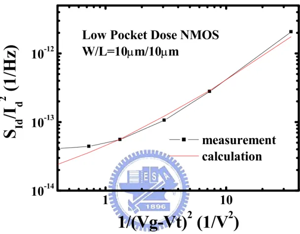
Fig. 3-7 Comparison of calculated and measured noise results for long channel length NMOS (W/L=10µm/10µm) with low pocket dose.
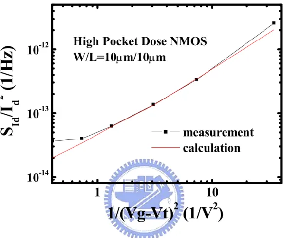
Fig. 3-8 Comparison of calculated and measured noise results for long channel length NMOS (W/L=10µm/10µm) with high pocket dose.
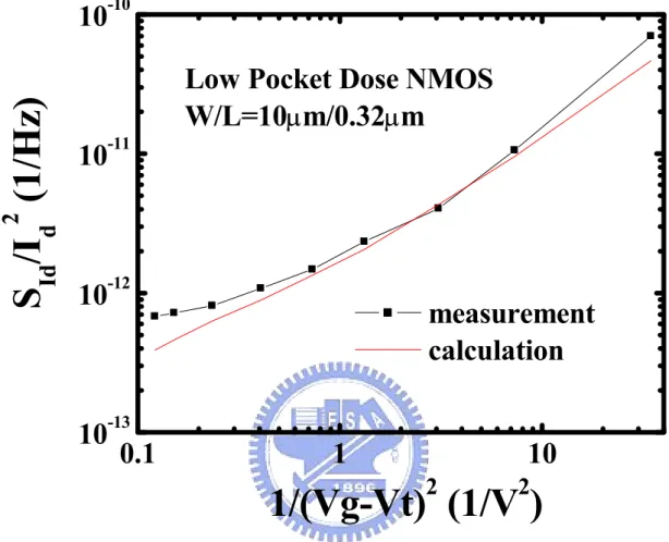
Fig. 3-9 Comparison of calculated and measured noise results for short channel length NMOS (W/L=10µm/0.32µm) with low pocket dose.
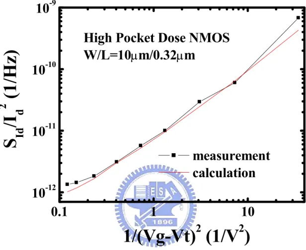
Fig. 3-10 Comparison of calculated and measured noise results for short channel length NMOS (W/L=10µm/0.32µm) with high pocket dose.
Fig. 3-11 The diagram of an n-type ONO charge storage cell. The VT distribution before and after CHE/FN programming is also shown. VT1 is the local threshold voltage below the CHE programmed region. ∆L is the width of the programmed region. VT2 is the threshold voltage of the fresh device. Fig. 3-12 Normalized noise characteristics (meas. @ linear regime) after CHE
programming (VT=0.8V) and BTBHH erasing in an n-type ONO charge storage cell. The noise increases after programming and goes back after erasing.
Fig. 3-13 Normalized noise versus Vg characteristics (meas. @ linear regime) after CHE programming and edge erasing in an n-type ONO charge storage cell. The noise seriously degrades at low Vg where the number fluctuation mechanism dominates.
Fig. 3-14 Normalized noise versus Vover-drive (Vg-VT) characteristics (meas. @ linear regime) after FN programming and erasing in an n-type ONO charge
Fig. 3-15 Modeling results of non-uniform threshold voltage effect. One can choose an optimal set of VT1 and ∆L to fit the measurement results based on the two-region model.
Fig. 3-16 Extraction of VT1 and ∆L by the error function method. The global
minimum (minimum error=0.03) is located at VT1=2.9V, ∆L=290Å in our CHE program condition.
Chapter 4
Fig. 4-1 The structure of an n-MOSFET for device simulation.
Fig. 4-2 Simulated carrier distribution of a non-pocket n-MOSFET at different depth in the channel region. The channel length is 1µm.
Fig. 4-3 Simulated carrier distribution of a pocket n-MOSFET at different depth in the channel region. The channel length is 1µm.
Fig. 4-4 Simulated carrier distribution of a non-pocket n-MOSFET at different depth in the channel region. The channel length is 0.18µm.
Fig. 4-5 Simulated carrier distribution of a pocket n-MOSFET at different depth in the channel region. The channel length is 0.18µm.
Fig. 4-6 Simulation of threshold voltage roll-off for different pocket splits. The pocket depth is 0.13µm.
Fig. 4-7 Simulation of threshold voltage roll-off for different pocket splits. The pocket depth is 0.1µm.
Fig. 4-8 Calculated normalized noise power spectral density for different pocket splits. The pocket depth is 0.13µm.
Fig. 4-9 Calculated normalized noise power spectral density for different pocket splits. The pocket depth is 0.1µm.
n-MOSFETs with L=1.2µm and 0.22µm.
Fig. 4-11 Comparison of substrate bias effect for different gate voltage in pocket n-MOSFETs with L=1.2µm and 0.22µm.
Fig. 4-12 Simulated carrier distribution of a non-pocket n-MOSFET at different depth in the channel region. The channel length is 1µm. The substrate bias is 0.5V. Fig. 4-13 Simulated carrier distribution of a non-pocket n-MOSFET at different depth in the channel region. The channel length is 1µm. The substrate bias is -1V. Fig. 4-14 Simulated carrier distribution of a non-pocket n-MOSFET at different depth
in the channel region. The channel length is 0.18µm. The substrate bias is 0.5V.
Fig. 4-15 Simulated carrier distribution of a non-pocket n-MOSFET at different depth in the channel region. The channel length is 0.18µm. The substrate bias is -1V.
Fig. 4-16 Simulated carrier distribution of a pocket n-MOSFET at different depth in the channel region. The channel length is 1µm. The substrate bias is 0.5V. Fig. 4-17 Simulated carrier distribution of a pocket n-MOSFET at different depth in
the channel region. The channel length is 1µm. The substrate bias is -1V. Fig. 4-18 Simulated carrier distribution of a pocket n-MOSFET at different depth in
the channel region. The channel length is 0.18µm. The substrate bias is 0.5V.
Fig. 4-19 Simulated carrier distribution of a pocket n-MOSFET at different depth in the channel region. The channel length is 0.18µm. The substrate bias is -1V.
Chapter 5
current interval between the two maximum number and the two peaks can be clearly symbolized as two-level RTS.
Fig. 5-2 Normalized noise power spectral density (at f=100Hz) versus gate oxide thickness in large area n-MOSFETs (W/L=10µm/1µm). The noise level has an abnormal increase in the 15Å oxide device.
Fig. 5-3 Temperature dependence of the 1/f noise in tox=15Å and 65Å n-MOSFETs (W/L=10µm/1µm). The noise is measured at Vd=0.2V.
Fig. 5-4 Measured and calculated Lorentzian-like noise power spectral density of a small area n-MOSFET (W/L=0.16µm/0.12µm, tox=15Å). The noise is
measured at strong inversion (Vd=0.2V, Vg=1.1V). The corner frequency (fc) is also shown in the figure.
Fig. 5-5 Temperature dependence of the Lorentzian-like noise in a small area n-MOSFET (W/L= 0.16µm/0.12µm, tox=15Å). The noise is measured at strong inversion (Vd=0.2V, Vg=1.1V). The peak of SId/Id2×f corresponds to the corner frequency.
Fig. 5-6 Arrhenius plot of trap time constant versus 1000/T. The linear behavior of the Arrhenius plot shows that the source of the noise is related to carrier capture process by an interface trap.
Fig. 5-7 The corner frequency versus gate voltage in a small area n-MOSFET (W/L=0.16µm/0.12µm, tox=15Å). A shallow trap (Et1) is observed in weak inversion (Vg<0.9V) and a deep trap (Et2) is in strong inversion (Vg>1.0V). Fig. 5-8 The substrate current (Ib) versus gate voltage in n-MOSFETs. The Ib in the
15Å oxide device drastically increases with Vg>1.0V (strong inversion regime), which indicates the occurrence of valence-band electron tunneling. Fig. 5-9 Diagram of valence-band electron tunneling induced substrate current (Ib) in
Fig. 5-10 The characteristics of two-level RTS at various gate voltages (in weak inversion) in a small area n-MOSFET (W/L=0.16µm/0.12µm, tox=15Å). RTS is undetectable at Vg=0.9V.
Fig. 5-11 Average τL and τH (extracted from RTS) versus gate voltage in weak inversion regime.
Fig. 5-12 (a) RTS in weak inversion condition. The RTS results from electron capture (τH) and electron emission (τL) at interface trap Et1. (b) RTS in strong inversion condition. The RTS results from electron capture (τL) and hole capture (τH) at Et2.
Fig. 5-13 The characteristics of two-level RTS at various gate voltages (in strong inversion regime) in a small area n-MOSFET (W/L=0.16µm/0.12µm, tox=15Å).
Fig. 5-14 Average τL and τH (extracted from RTS) versus gate voltage in strong inversion regime.
Fig. 5-15 The electron occupation factor (ft) and normalized noise power spectral density versus gate voltage in a small area n-MOSFET (W/L= 0.16µm/0.12µm, tox=15Å). The second noise peak in strong inversion is due to valence-band electron tunneling.
Fig. 5-16 Electron occupation factor (ft) and normalized noise power spectral density in a small area tox=65Å n-MOSFET (W/L= 0.16µm/0.24µm,).
Table Captions
Chapter 3
Table 3-1 The values of pocket length, threshold voltage and oxide trap density for low/high pocket doses.
Table 3-2 Comparison of the two extraction method: 1. reverse engineering and 2. extraction by flicker noise measurement.
List of Symbols
Chapter 2
drain current noise power spectrum density
input referred gate voltage noise power spectrum density
carrier mobility
mobility limited by oxide charge scattering mobility limited by other scattering mechanisms electron charge
channel carrier density horizontal electric field total trap density oxide trap density interface trap density
trap density in the depletion region inversion layer capacitance
depletion layer capacitance interface trap capacitance scattering coefficient
trap occupation function (factor) electron quasi-Fermi level trap time constant
time constant at the interface attenuation coefficient transconductance
S
IdS
Vgµ
effq
N
E
xN
tN
oxN
itN
dC
iC
dC
itµ
oxµ
nα
f
tE
fnτ
τ
0γ
g
mChapter 3
normalized noise power spectrum density effective channel length
threshold voltage
Chapter 4
Pocket Length
channel doping concentration
Chapter 5
corner frequency
energy barrier for the capture of an carrier trap energy
S
id/I
d 2L
effV
tL
pD
cf
c∆E
bE
tChapter 1
Introduction
The CMOS technology, which possesses the advantage of low cost, high integration, and low power, is finding more and more important applications in the area of analog IC. The capability of integrating analog and digital circuits on the same chip is crucial to the production of high-performance MOS integrated circuits such as telecommunication circuits [1-1]. Nevertheless, there is a major drawback in analog applications. Compared with bipolar transistors, MOS transistors are so noisy, especially in the low frequency region where the flicker noise dominates [1-2]. Flicker noise will affect the signal-to-noise ratio (SNR) in operational amplifiers and in A/D and D/A converters. Phase noise of VCO originating from flicker noise is another concern for RF applications [1-3]. In order to reduce low frequency noise in analog devices, the physical origin of flicker noise in today’s CMOS devices should be further explored.
Studies of hot carrier degradation on low frequency noise indicate that this quantity is extremely sensitive [1-4,5,6]. E. Simoen showed that the increase of the noise spectral density follows a t0.3 power law dependence with stress time in a 0.7µm CMOS technology [1-5] and that the RTS amplitude of a particular oxide trap increased after hot carrier stress in 0.5µm×0.5µm p-MOSFETs [1-6]. Some studies show that the low-frequency 1/f noise is correlated with oxide-trapped charge and that the high-frequency 1/f noise is correlated with interface traps [1-7]. Following up these hot carrier degradation effects, we proposed that non-uniform threshold voltage distribution induced by local oxide charges plays an important role on the dominant source of flicker noise.
As we know, pocket implantation in a CMOS process is a key method to reduce the sub-threshold leakage in logic devices. However, it has some drawbacks, such as the increase of drain-substrate coupling, poor Early voltage, lower high frequency output resistance [1-8]
and increased non-linearity [1-9], in analog applications. Recent study has shown that pocket implantation will also degrade drain current flicker noise. The new structure, such us single pocket or asymmetric channel structure [1-8,10] and epitaxial channel MOSFETs [1-11,12], is proposed to have better noise performance because of the elimination of pocket implantation process. Although some researchers attributed the increase of noise to additional oxide trap creation by pocket implantation [1-12], the real cause of pocket implantation induced noise degradation is still not clear.
The purpose of this study is to investigate pocket implantation effect on flicker noise in n-MOSEFTs with various pocket doses and device dimensions. It is suggested that the pocket implantation will change the threshold voltage distribution, so that the noise characteristic is also affected. An analytical flicker noise model taking into account a pocket doping effect will be proposed. In addition, this analytical model can be included into circuit simulators, such as HSPICE, to improve the model accuracy.
In addition to the analytical noise model, we use a two-dimensional device simulator, MEDICI, to simulate the effects of channel carrier distribution on flicker noise. The substrate bias and pocket implantation doping profile is changed to verify the relation between channel carrier distribution and drain current flicker noise.
From now on, the origin of low frequency flicker noise in MOSFETs with relatively thick gate oxides has been extensively studied. A unified noise model [1-13] based on oxide charge tunnel trapping and de-trapping has been adopted. The carrier number and mobility fluctuation induced from trapped oxide charges is thought to be the source of flicker noise. In addition, some studies showed that the low frequency noise may result from charge emission and capture at interface traps in weak inversion condition or in the very high frequency regime of noise power spectral density [1-14]. As gate oxide thickness is scaled into direct tunneling domain, oxide trap density should be much reduced. In addition, channel electrons would likely tunnel through an ultra-thin gate oxide directly without being captured by oxide
traps. However, the low frequency noise in ultra-thin oxide CMOS devices still exhibits a significant level [1-15,16]. The traditional oxide charge tunnel trapping and de-trapping concept seems no longer suitable to explain the noise behavior in ultra-thin oxide MOSFETs.
In addition to the discussions of flicker noise on frequency domain, the time domain presentation of low frequency noise is known as random telegraph signal (RTS) and has been studied in past decades [1-17,18,19,20]. Due to a single charge trapping and de-trapping in a small area device, RTS exhibits two levels. The upper level corresponds to an empty trap, i.e., no electron occupation, and the duration of time is denoted by τH. The lower level corresponds to an electron occupied state and is denoted by τL. In many cases, τH corresponds to the time it takes to capture a carrier, while carrier release (emission) from traps governs τL [1-21]. In the ultra-thin oxide case, we will study the τL and τH behavior instead of the noise behavior in frequency domain. Based on the time domain analysis, a new noise generation model for ultra-thin oxide device is proposed.
Organization of This Thesis
This thesis is organized into six chapters.
In chapter 1, we give a brief introduction about this thesis.
In chapter 2, the hot carrier effect on drain current flicker noise is investigated. Conventional 0.18µm technology CMOS devices and a special ONO charge storage cell are used in this work. The channel length from 0.22µm to 2µm, and a 10µm gate width is used. An ONO cell with 90Å effective gate oxide thickness, 0.58µm channel length, and 1 µm gate width is used to verify the source of degradation. Maximum substrate and gate current stress, FN stress, and double side maximum gate current stress are performed in these devices. All the noise data are measured at linear region. The input referred noise power spectral density (SVG) is used as a monitor of noise degradation, which provides fairer comparison.
The input/output n-MOSFETs of a 0.13µm CMOS technology is used in this work. The I/O devices have a 5.8nm gate oxide, a gate length from 0.22µm to 10µm, and a gate width of 10mm. Two pocket implant doses were used. Each noise measurement data point represents an average of 3 to 10 devices. The normalized noise power spectrum density (Sid/Id2) is chosen as a monitor of drain current noise, which is considered to be a fair index because of the normalization to the drain current. In addition, charge pumping measurement is performed to characterize oxide (interface) trap density for different pocket implant splits.
In Chapter 4, the simulation of the effect of inversion carrier distribution variation on flicker noise through different applied substrate bias and pocket doping profile are investigated. The two-dimensional device simulator, MEDICI, is used.
In Chapter 5, the low frequency noise in a 15Å gate oxide n-MOSFET is investigated. The electron trapping and de-trapping times (τH and τL) are characterized from RTS in a small area n-MOSFET. The normalized noise power spectral density (Sid/Id2) is measured as a monitor of drain current noise, which is considered as a fair index because of the normalization to the drain current. In addition, the RTS time constants and noise power spectral density in n-MOSFETs with 33Å gate oxide are also characterized for comparison. The drain bias in RTS and noise measurement in this study is 0.1V to ensure a uniform charge distribution in the channel. Finally, a new noise source due to valence band electron tunneling will be proposed to explain the observed noise behavior.
Chapter 2
Hot Carrier Effect on Drain Current Flicker Noise
in Analog n-MOSFETs
2.1 Introduction
Because of its low cost, high integration, and low power, the CMOS technology is finding more and more important applications in the area of analog IC. The capability of integrating low-cost analog circuits and high-speed digital circuits on the same chip is crucial to the production of high-performance MOS integrated circuits such as A/D converters and telecommunication circuits [2-1]. Nevertheless, there is a major drawback in analog applications. Compared with bipolar transistors, MOS transistors are so noisy, especially in the low frequency region where the flicker noise dominates [2-2]. In order to optimize low frequency noise performance in analog applications, the need for further understanding of the noise characteristics of MOS transistors is obvious. In addition, hot carrier degradation is known to significantly increase the flicker noise amplitude of MOS transistors in the linear mode [2-3]. So as to improve the MOS circuit’s performance, a device designer has to understand the physical origin of flicker noise.
At present, there are two major theories to explain the physical origins of flicker noise in MOS transistors. One is the number fluctuation theory based on the McWhorter’s charge trapping model; the other is the bulk mobility fluctuation theory based on Hooge’s hypothesis [2-2]. C. Hu et al. have developed a unified flicker noise model, which incorporated both the number fluctuation and the correlated surface mobility fluctuation mechanisms [2-1,4,5]. Several studies had shown that the flicker noise in n-MOSFETs is dominated by the number fluctuation mechanism [2-6,7,8]; based on this mechanism, the input referred gate voltage noise power spectrum density (SVg) would be independent of gate bias. On the other hand, the noise is mainly due to the mobility fluctuation mechanism, which suggests gate voltage
dependence in SVg, in p-MOSFETs [2-9,10].
Studies of hot carrier degradation on the low frequency noise indicate that this quantity is extremely sensitive [2-11,12,13]. E. Simoen showed that the increase of the noise spectral density follows a t0.3 power law dependence with stress time in a 0.7µm CMOS technology [2-14]. In addition, the RTS amplitude of a particular oxide trap increased after hot carrier stress in 0.5µm×0.5µm p-MOSFETs [2-13]. Some studies show that the low frequency noise is correlated with oxide-trapped charge and that the high-frequency noise is correlated with interface traps [2-14]. Toshiba Corp. proposed an epitaxial channel MOSFET (without halo implantation) for lower interface traps and better flicker noise performance [2-15].
The purpose of this study is to find out the real source responsible for hot carrier degradation through various kinds of stresses. We will show that non-uniform threshold voltage distribution, which is induced from local oxide charge generation after stressing, along the channel will cause noise degradation. Using this concept as a basis, a device designer can optimize the flicker noise performance through substrate engineering.
2.2 Basic Theory of Flicker Noise
Flicker noise was observed in vacuum tubes by Johnson in 1925 and interpreted by Walter Schottky in 1926. In the present day, flicker noise is found in all active devices [2-2], such as Si BJT, MOSFET, and SiGe HBT. The power spectrum density of such noise often varies as f-1 with energy concentrated at low frequencies. Therefore, it is called 1/f noise or low frequency noise as well.
In the past, there were two major models to explain the mechanisms of flicker noise in MOSFETs- McWhorter’s [2-16] charge trapping model and Hooge’s empirical relation [2-17], but no connection between two models had been explored. According to the carrier number fluctuation theory proposed by McWhoter, flicker noise is explained by the fluctuation of the channel free carrier due to the random capture and emission by the oxide traps near the
Si-SiO2 interface. Either the surface potential fluctuation resulting from charge fluctuation or the charge exchange between the channel and the oxide traps induces the current fluctuation. Mathematically each oxide trap near the interface provides Lorentzian [2-4] spectrum. For the uniform oxide trap distribution in the bandgap, each Lorentzian component adds up to 1/f noise spectrum. On the other way, the mobility fluctuation theory based on Hooge’s hypothesis regards the flicker noise as a consequence of bulk mobility fluctuation; moreover, the fluctuation of bulk mobility in MOSFETs is caused by phonon population through phonon scattering [2-18]. However either theory couldn’t verify the noise generation mechanism independently and completely. At present, C. Hu’s Unified Flicker Noise Model [2-1,4] has become the main stream to elucidate the origin of flicker noise. They develop I-V and noise models to incorporate both number fluctuation theory and bulk mobility fluctuation theory.
The unified flicker noise model combined number and mobility fluctuation models through the I-V model [2-1,4]. The drain current Id in strong inversion for a MOSFET with width W and length L is given by
I
d=
W
µ
effqNE
x (2-1)where µeff is the carrier mobility, and q is the electron charge, N is the number of channel carriers per unit area, and Ex is the horizontal electric field. In addition, consider a section of channel with width W and length ∆x. Fluctuation in the amount of trapped oxide charge will induce correlated fluctuations in the carrier number and mobility. The result fractional charge in the local drain current can be expressed as
t t eff eff t d d
N
N
N
N
N
I
I
⎟
⎟
∆
⎠
⎞
⎜
⎜
⎝
⎛
∆
±
∆
∆
∆
=
δ
δ
δµ
µ
δ
δ
δ
1
1
(2-2)where Nt is the number of occupied traps per unit area, ∆N=NW∆x and ∆Nt =NtW∆x. The sign in front of the mobility fluctuation term in Eq. (2-2) is chosen according to whether the trap is neutral or charged when filled. The ratio of the fluctuations in the carrier number to fluctuations in occupied trap number, R=δ∆N/δ∆Nt, is close to unity at strong inversion.
The ratio R can be expressed as d it ox t
N
N
N
N
N
N
N
R
+
+
+
−
=
∆
∆
=
δ
δ
(2-3) where Nox ,Nit and Nd are oxide trap density, interface trap density and trap density in the depletion region. Through the relation C=βqN, a general expression for R isd it ox i i
C
C
C
C
C
R
+
+
+
−
=
(2-4)where Ci, Cd and Cit are inversion layer, depletion layer, and interface trap capacitances. To evaluateδµeff /δ∆Nt, we need to know the relation between carrier mobility and oxide
charge density, which based on Matthiessen’s rule: t n ox n eff
N
α
µ
µ
µ
µ
=
+
=
+
1
1
1
1
(2-5)where µox is the mobility limited by oxide charge scattering, µn is the mobility limited by other scattering mechanisms, and α is the scattering coefficient with a typical value of
Vs
15
10
2× − . On the basis of Eq. (2-5) it can be shown that
x
W
N
eff t eff∆
−
=
∆
2αµ
δ
δµ
(2-6)Substituting Eq. (2-4) and Eq. (2-6) into Eq. (2-2) yields
x
W
N
N
I
I
t eff d d∆
∆
⎟
⎠
⎞
⎜
⎝
⎛
±
−
=
αµ
δ
δ
1
(2-7)Hence, the power spectrum density of the local current fluctuations is
(
,
)
1
)
,
(
2 2f
x
S
N
x
W
I
f
x
S
d eff Nt Id ∆ ∆⎟
⎠
⎞
⎜
⎝
⎛
±
⎟
⎠
⎞
⎜
⎝
⎛
∆
=
αµ
(2-8)whereS∆Nt( fx, )is the power spectral density of the mean-square fluctuations in the number of occupied traps over the area W∆x. According to the conventional theory of number fluctuations, )S∆Nt( fx, is given by
(
)
(
)
(
)
(
)
(
E
x
y
z
)
dzdydE
z
y
x
E
f
xf
z
y
x
E
N
f
x
S
E t t t E W t Nt c v ox 2 2 0 01
,
,
,
,
,
,
1
,
,
,
4
,
τ
ω
τ
+
−
∆
=
∫ ∫ ∫
∆ (2-9)where
N
t(
E
,
x
,
y
,
z
)
is the distribution of the traps in the oxide and over the energy,)
,
,
,
(
E
x
y
z
τ
is the trapping time constant, =[
1+exp( − )/]
−1kT E E
ft fn is the trap occupancy
function, Efn is the electron quasi-Fermi level, is the angular frequency, tox is the oxide thickness, and Ec-Ev is the silicon bandgap. In order to evaluate the integral in Eq. (2-9), we make two assumptions: 1) The oxide traps have a uniform spatial distribution near the interface, consequently, Nt(E,x,y,z)= Nt
( )
E . 2) The probability if an electronpenetrating into the oxide decreases exponentially with the distance from the interface, thus the trap time constant is given by
τ
=
τ
0(
E
)
exp(
γ
z
)
(2-10)where τ0(E) is the time constant at the interface, and γ is the attenuation coefficient of the electron wave function in the oxide with a value of 108cm-1 [2-1,4]. Since ft(1− ft)in Eq. (2-9) behaves like a delta function around the quasi-Fermi level, traps level around Efn is the major contribution to the integral. ThereforeNT(E)can be approximated byNT(Efn)and ft(1− ft)
can be replace by−kTdfT /dE. Then solve the integration yields
f
x
kTW
E
N
f
x
S
Nt t fnγ
∆
=
∆(
,
)
(
)
(2-11)The total drain current noise power spectrum turns out to be
( )
dx x N E N fWL kTI xdx f x S L f S L d L t fn Id Id∫
∫
⎥ ⎦ ⎤ ⎢ ⎣ ⎡ ± = ∆ = ∆ 0 2 2 2 0 2 1 ) ( ) , ( 1 ) (αµ
γ
(2-12)where L is the channel length. Eq. (2-12) is the basic expression of the unified flicker noise model. In strong inversion with very low drain voltage, the carrier density is uniform along the channel. Then Eq. (2-12) simplifies as
( ) 1 ( ) 2 2 fn t d Id N E N fWL kTI f S ⎟ ⎠ ⎞ ⎜ ⎝ ⎛ + =
αµ
γ
(2-13)Due to the fluctuation of the drain current, the input referred noise power is given by
(
)
( )
2(
1
)
2(
)
2 2 T fn OX m id VgN
N
E
fWLC
kTq
g
f
S
f
S
αµ
γ
+
=
=
(2-14)where gm is the transconductance (gm =δId/δVG =WµCoxVd/L) and Vd is the drain voltage.
2.3 Device Information and Experimental Setup
Conventional 0.18µm technology CMOS devices and a special ONO charge storage cell are used in this work. In order to emphasize the oxide traps storage capability, CMOS devices with 65Å gate oxide thickness are used. According to a statistical evaluation of the flicker noise, devices with too small area may have a large fluctuation range [2-19], so the channel length from 0.22µm to 2µm, and a 10µm gate width is used. An ONO cell with 90Å effective gate oxide thickness, 0.58µm channel length, and 1µm gate width is used to verify the source of degradation. Maximum substrate and gate current stress, FN stress, and double side maximum gate current stress are performed in these devices. All the noise data are measured at linear region. The input referred gate voltage noise power spectrum density (SVg) is used as a monitor of noise degradation, which provides fairer comparison. The flicker noise measurement system (100Hz~100KHz) involves a HP4155 semiconductor parameter analyzer, a BTA9603 FET noise analyzer, and a SR780 network signal analyzer. All measurement is controlled automatically through GPIB cards by a computer program named BTA-NoisePro. The block diagram of noise measurement system is shown in Fig. 2-1.
2.4 Flicker Noise Degradation under Different Stress Condition in Analog
n-MOSFETs
The source responsible for drain current flicker noise degradation in n-MOSFETs is studied. When the device suffers from hot carrier effects, interface states or oxide traps will be generated. We will verify how they alter the noise behavior by various stress modes. The SVg
is used as a monitor of degradation before and after stressing. Compared to SId, it provides fairer comparison as the drain current is normalized. All noise measurements are biased at low gate voltage in the linear region to assure that number fluctuation mechanism dominates the noise behavior.
2.4.1 Maximum Substrate Current Stress
Fig. 2-2 shows the n-MOSFET (W/L=10µm/0.34µm, tox=65Å) Id-Vg characteristics before and after hot-carrier stress. The stress bias is at Vg=1.64V, Vd=3V, where the maximum substrate current (Ib) occurs. For maximum Ib stress, both interface states and neutral electron traps are generated in the oxide, with the former being dominant. The subthreshold swing degradation is then due to the generation of interface state. The SVg measured at Vd=0.1V and Vg=1.0V before and after maximum Ib stress are shown in Fig. 2-3. However, the noise remains the same after stressing. That is, the generation of fast interface states will not degrade the flicker noise behavior in the frequency range from 100Hz to 100kHz.
2.4.2 Maximum Gate Current Stress
Fig. 2-4 shows the n-MOSFET (W/L=10µm/0.34µm, tox=65Å) Id-Vg characteristics before and after hot-carrier stress. The stress bias is at Vg=4.7V, Vd=4.7V, where the maximum gate current (Ig) occurs. After stressing, there are some local electron traps generated near the drain side. The threshold voltage shifts about 0.3V after stressing. The SVg measured at Vd=0.1V and Vg=1.0V before and after maximum Ig stress are shown in Fig. 2-5. Comparably, the noise increases about an order in the entire range of measurement frequency. These local oxide-trapped charges, which generate non-uniform threshold voltage distribution along the channel, are the source responsible for hot-carrier degradation of flicker noise.
2.4.3 Fower-Nordheim Stress
Fig. 2-6 shows the n-MOSFET (W/L=10µm/0.34µm, tox=65Å) Id-Vg characteristics after FN stress (stress bias: Vg=8V). We precisely control the stress time so that the threshold voltage shift remains the same (0.3V) with maximum Ig stress. In addition, the sub-threshold swing slightly degrades. That is, there are uniform electron traps and a little amount of interface states generating along the channel. The SVg measured at Vd=0.1V and Vg=1.0V before and after maximum Ig stress are shown in Fig. 2-7. The noise slightly increases after FN stress. This can be explained by the increase of oxide traps density, so that the probability of trapping/de-trapping increases. And we will show that the uniform oxide-trapped charges will not alter the noise latter.
2.5 Flicker Noise Degradation under Different Stress Condition in Special
ONO Charge Storage Cells
In order to make sure the dominant noise degradation source is the non-uniform oxide-trapped charges, a special n-type ONO charge storage cell, which doesn’t generate extra oxide traps after hot-carrier stress, is used. The ONO cell structure is shown in Fig. 2-8(a), and the channel length is 0.58µm, the gate width is 1µm, and the gate oxide thickness is 90Å.
2.5.1 Fower-Nordheim Programming
Fowler-Nordheim (FN) program is used for this cell to create uniform nitride charges with negligible generation of oxide traps. Fig. 2-9 shows the ONO cell (W/L=1µm/0.58µm) Id-Vg characteristics after FN programming (program bias: Vg=15V, others 0V). The parallel shift in Fig. 2-9 is attributed to negative trapped charge in the nitride layer. Fig. 2-10 shows the results of noise degradation after FN programming. The noise is measured at linear operation regime. As can be seen, the threshold voltage shifts about 0.5V, and the noise remains just the same as the fresh device. This implies that the generation of uniform electron
traps along the channel doesn’t degrade the SVg.
2.5.2 Maximum Gate Current Programming
Channel hot electron injection and band-to-band hot hole injection are utilized for programming and erasing to generate local oxide charges. Fig. 2-11 shows the ONO cell (W/L=1µm/0.58µm) Id-Vg characteristics after maximum Ig programming (program bias: Vd=4V, Vg=6.5V) and hot hole erasing (erase bias: Vd=7V, Vg=-3V). Fig. 2-12 illustrates the noise behavior after the generation of non-uniform threshold voltage distribution. The noise is measured at linear operation regime. After hot-carrier programming, the noise increases about an order, and the noise turns back after drain-side erasing. So far, it is proved by ONO cell that non-uniform threshold voltage distribution caused from local oxide-trapped charge can seriously enhance the flicker noise.
2.6 Two-Region Model of Noise Degradation
In order to clarify the local oxide charge enhanced flicker noise degradation, the non-uniform threshold voltage method, also called two-region method, is used [2-20]. The effects of channel non-uniformity can be simplified as a MOSFET with two regions of different threshold voltage [2-21]. For the case of maximum Ig stress in an n-MOSFET as shown in Fig. 2-8(b), the higher threshold region (Region 1) near the drain is due to channel-hot electron stress and the lower one (Region 2) is the rest of channel.
The drain voltage and the corresponding noise power for a two-region MOSFET can be modeled as [2-22]
V
d=
V
1+
V
2 (2-15) thus
S
Vd(stress)=
S
V1+
S
V2 (2-16)have 2 2 2 2 1 1 2 ) (
(
)
(
)
(
)
G
f
S
G
f
S
G
f
S
Id stress I I+
=
(2-17) where i i i i L W QG = µ is the channel conductance associated with region i,
1 1 2 1 1 ) ( − + − − = G G
G is the total current conductance and Id=I1=I2 is the drain current. Assume that the transconductance is constant along the channel, thus the input referred noise power is given by 2 2 2 2 1 1 2 ) ( ( ) ( ) ( ) G f S G f S G f S Vg Vg stress Vg + = (2-18)
Because of the higher threshold voltage in Region 1 than in Region 2, it follows that
2 1 1 1 2 2
G
G
L
Q
L
Q
>>
⇒
>>
(2-19) Consequently, 2 2 2 2 1 1(
)
(
)
G
f
S
G
f
S
Vg Vg>>
(2-20) andG
≈
G
1 (2-21)Accordingly, the equivalent total input referred power of the two components can be simplified as
S
Vg(stress)(
f
)
=
S
Vg1(
f
)
(2-22) The noise from Region 1 will dominate, and the total input referred power after maximum Ig stress is given by(
)
(
1
)
1(
1)
2 1 1 1 2 2 ) ( T f OX stress VgN
N
E
WL
fC
kTq
f
S
αµ
γ
+
=
(2-23)
⎥
⎥
⎦
⎤
⎢
⎢
⎣
⎡
⎟⎟
⎠
⎞
⎜⎜
⎝
⎛
≈
)
(
)
(
)
(
)
(
1 1 ) ( fn t fn t Vg stress VgE
N
E
N
L
L
f
S
f
S
(2-24) The net result can drastically enhance gate voltage noise due to not only a smaller L1 but also a large Nt1(Ef1). As a consequence, the non-uniform distribution of the threshold voltage along the channel, such as in maximum Ig stressed device, may enhance serious degradation of the 1/f noise. In contrast, the uniform oxide charge generated by FN stress couldn’t cause significant increase of the 1/f noise.2.7 Summary
The hot carrier degradation mechanisms of drain current flicker noise in analog CMOS devices are investigated. The sources responsible for noise degradation are verified through both submicron CMOS transistors and a special ONO charge storage cell with various kinds of stresses. From our observation, the non-uniform oxide-trapped charges generated by maximum gate current stress could give rise to series flicker noise degradation as the number fluctuation mechanism dominates noise processes, which can be understood through a two-region unified flicker noise model. For n-MOSFETs, the number fluctuation mechanism dominates at low gate bias, so that the noise magnitude seriously increases after hot carrier stressing.