High-Output-Current and Low-Power-Loss Mobile Thin-Film Transistor Liquid-Crystal Display Driver
K. T. Mok
∗, Y. M. Lai
†Department of Electronic and Information Engineering The Hong Kong Polytechnic University
Hung Hom, Hong Kong, China
∗Email: 05228669d@net3.eie.polyu.edu.hk
†Email: enymlai@polyu.edu.hk
W. C. Chan
‡, C. F. Lee
§ Solomon Systech Limited 6/F., No.3 Science Park East Avenue,Hong Kong Science Park, Shatin, N.T., Hong Kong, China
‡Email: wcchan@solomon-systech.com
§Email: cflee@solomon-systech.com
Abstract—System-on-chip (SoC) mobile thin-film transistor (TFT) liquid-crystal display (LCD) drivers are, to a certain extent, inadequate to support portable devices that require higher driving currents for their high resolution and large LCD panels.
In this paper, we will show how a simple boost converter can be designed and used in the display driver for high current demand TFT-LCD panels. The proposed driver circuit is partitioned in a way that the current chip-on-grass (COG) package technology used by the traditional mobile display driver can be maintained in order to save production cost. A prototype of the controller of the proposed power converter is designed with a standard 0.13-µm HV CMOS process. Compared with traditional designs, the proposed circuit shows its support on higher output currents with improved power efficiency and output voltage variation.
Index Terms—Thin-film transistor (TFT), liquid-crystal dis- play (LCD), chip-on-grass (COG), indium-tin-oxide (ITO), boost converter.
I. INTRODUCTION
The voltage doubler inside the power system of traditional mobile TFT-LCD drivers is designed to deliver an output current of 1 to 3mA [1]. Those display drivers are mainly used in portable devices such as mobile phones and MP3 players that have relatively small display panels. The conduction loss of undesirable indium-tin-oxide (ITO) parasitic resistances (RITO), due to COG package technology, in these devices is not significant and is usually ignored. However, in view of the ever-increasing demand from the consumer electronics industry for large and high-resolution display panels, the traditional voltage doubler designs are no longer adequate. The large panels require a current at least of 5 to 20mA to power for proper operations. In such high current applications, the conduction losses can no longer be ignored as it may lead to the output voltage regulations, panel visual performance and power efficiency issues.
This paper shows how a simple boost converter can be designed to replace the traditional voltage doubler circuit used in the power system of mobile TFT-LCD drivers to meet high current output demand while the current COG package technology need not to be changed. The controller IC of the proposed circuit is fabricated using a standard 0.13-µm HV CMOS process with the die size 1083 µm × 583 µm. The
Power System
System Interface GDDRAM Gamma Voltage
Generator Source Drivers Gate Drivers
Com Buffer
Timing and Voltage Level Control Logic VCHVCLVGHVGLVS
VCIX2
VDD
VDD
VCI
To LCD To LCD To LCD
VDD
Fig. 1. Functional block diagram of a conventional SoC mobile TFT-LCD driver.
simulation and measurement results proved that the power efficiency reaches 85% and it can maintain a constant 6 V output voltage with the output current from 5 to 20 mA.
II. REVIEWOFMOBILETFT-LCD DRIVERSANDITS
LIMITATION
The functional block diagram of a conventional SoC mo- bile TFT-LCD driver is shown in Fig. 1, where the gate driver, source driver, common electrode driving buffer (COM buffer), data and timing controller, graphic display data RAM (GDDRAM) as well as the power system are integrated in a single-chip IC. The power system in the TFT-LCD drivers requires the generation of different voltage levels, including the gate driver on/off signals (VGH,VGL), source driver signal (VS) and high/low COM buffer signal (VCH, VCL), for the power sources of different functional blocks. Fig. 2 shows the block diagram of this power system, which consists of several step-up voltage and polarity inverted converters that usually implemented by using the switched-capacitor (charge-pump) topology. The voltage doubler (2X charge pump) supplies the power for source drivers and COM buffer, which consume most of the power of the TFT-LCD system while other charge
-6x charge pump
LDO -1x charge pump
LDO 2x charge pump
LDO 4x charge pump
LDO
6x charge pump LDO
VCI
(2.7 – 3.3 V)
VGH(14 – 18 V)
VS(4 – 6 V)
VCH(4 – 6 V)
VGL(-16 – -14 V) VCL(-2 – 0 V) VCIX2
Fig. 2. Block diagram of this power system in a mobile TFT-LCD driver.
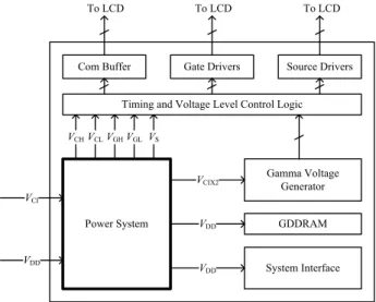
TFT-LCD Driver IC External Components
FPC ITO
Fig. 3. Illustration diagram to show the location of the ITO.
M8
M7
M4
M3
M6
M2
M1
RITO
Cfly Cfly’ COUT
RITO
M5
RITO
RITO
RITO
RITO
VIN
RITO Φ1
Φ1
Φ2
Φ2
Φ2
Φ2
Φ1
Φ1
On chip components
Off chip components
VOUT
Fig. 4. Schematic of a traditional 2X charge pump with ITO parasitic resistance.
pumps with higher conversion ratios supply a relatively small amount of power for gate driver only. Hence, the performance of the voltage doubler significantly affects the power efficiency of the whole system.
The COG technology is usually used to package the display driver for minimizing the size of the display module [2]–[3]. In order to reduce the production cost, manufacturers design the display driver in such a way that the charge pump controller and the power switches are integrated in the display driver IC.
The storage and flying capacitors are usually located externally to maximize the charge pump performance [4]. Hence, those capacitors are connected to the IC through an ITO glass using flexible printed circuit (FPC) (Fig. 3).
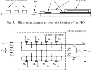
The schematic diagram of a traditional dual-phase 2X charge pump is shown in Fig. 4, where Φ1 andΦ2 are 50% non-overlapping out-of-phase clocks, Cfly and Cfly’ are the flying capacitors andCOUTis the output storage capacitor. As indicated in Fig. 4, undesirable parasitic resistances (RITO) of about 5 to 15Ω per connection exist between the IC and each external circuit components.
The traditional 2X charge pumps are designed to deliver a current of 1 to 3 mA to the display driver. It is used mainly in portable devices such as mobile phones and MP3 players.
The conduction loss due to RITO in these devices is not significant and is usually ignored. However, due to the ever- increasing demand from the consumer electronics industry, the higher resolution and larger size panels are highly demanded.
Furthermore, the portable media application, such as mobile TV, portable media players (PMP), global positioning system (GPS) devices, becomes popular [5]-[7]. Those large panels require the 2X charge pump to deliver an output current at least of 5 to 20mA for proper operations. Hence, the conduction losses can no longer be ignored. Moreover, without modifying the present power system circuit topology, the traditional charge pump designs cannot deliver adequate power to drive the large panels. Therefore, this paper will demonstrate how a simple boost converter can be designed to be incorporated into the display driver IC that meets the current demand for large display panels with improved power efficiency without the change of the existing COG package technology.
III. THEPROPOSEDHIGH-CURRENTLOW-POWERLOSS
DISPLAYDRIVER
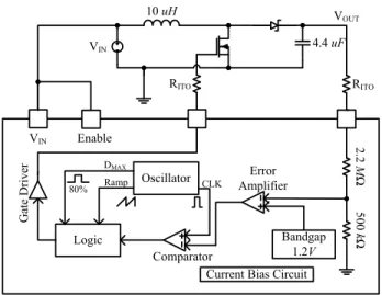
The proposed driver circuit must be able to provide a higher current output with reduced power loss while maintaining the use of COG package technology. The boost converter topology is chosen in the design to maintain the output voltage of 6 V with 5 to 20 mA output current. The converter circuit is partitioned so that the feedback controller of the converter is integrated in the display driver IC for reducing production cost. The power stage circuitry, including the inductor, power switch, diode and storage capacitor, of the converter is placed on a FPC next to the display driver IC. In this way, the power loss that dissipated inRITO can now be minimized. In order to further simplify the design, the boost converter is designed with voltage mode control and operated in discontinuous conduction mode (DCM) [8]. In this way, the effect of the right half plane zero of the control-to-output converter transfer function can be removed and the compensation network can be greatly simplified to save IC silicon area. Besides, regarding the electromagnetic interference (EMI) issue, the fix switching frequency pulse-width modulation (PWM) control scheme is superior to the variable switching frequency pulse-frequency modulation (PFM) one, as the former can provide a stable and predictable EMI noise performance. Moreover, the inductor size can be greatly reduced when operated in DCM. Fig. 5 shows the size of the inductor and other circuit components.
The block diagram of the proposed boost converter is shown in Fig. 6 and the specifications are shown in Table I. The controller design is based on 0.13-µm HV CMOS process with 6 V mid-voltage devices. The controller consists of an error amplifier, comparator, gate buffer, ramp signal and clock generator with build-in RC circuit, bandgap reference, feedback resistors and temperature independent current bias circuit.
IV. SIMULATIONANDMEASUREMENTRESULTS
After layout extraction, HSPICE simulations were con- ducted by using fabrication foundry’s device models together
TABLE I
SPECIFICATIONSOFTHEPROPOSEDCIRCUITANDITSCONTROLLER
Proposed boost converter specification
Output voltage 6V
Input voltage range 2.7 - 3.3V (nominal 3 V)
Inductor value 10µH
Capacitor value 4.4µF
Output current range 5 - 20mA Output power range 30 - 120mW
Proposed controller specification
Switching frequency 500kHz
Error amplifier DC gain: 41dB First pole: 112 kHz Ramp signal swing Low: 0.5V High: 1.5 V
Fig. 5. Prototype of the power stage circuit.
2.2 MΩ500 kΩ
RITO RITO
VIN
10 uH
4.4 uF
Logic
Oscillator
VOUT
Bandgap 1.2V Current Bias Circuit
Error Amplifier
Comparator
Gate Driver
VIN Enable DMAX
Ramp CLK
80%
Fig. 6. Block diagram of the proposed circuit.
with the manufacturer’s MOSFET switch and diode model for the comparison of the performance between the proposed circuit and a traditional charge pump. According to the speci- fications from manufacturers, the equivalent series resistances are set to be 0.6 Ω and 50 mΩ in the inductor and capacitor respectively. The parasitic ITO resistance is assumed to be
5 10 15 20
60 65 70 75 80 85 90 95 100
Output Current (mA)
Efficiency (%)
Charge Pump Proposed CIrcuit
Fig. 7. Simulated power efficiency of the proposed circuit and the traditional charge pump.
5 10 15 20
3 3.5 4 4.5 5 5.5 6 6.5
Output Current (mA)
Output Voltage (V)
Charge Pump Proposed CIrcuit
Fig. 8. Simulated output voltage of the proposed circuit and the traditional charge pump.
10Ω.
As shown in Fig. 7, when the output current increases from 5 to 20 mA, the simulated power efficiency of the charge pump decreases dramatically from around 90 % to 70 % while that of the proposed circuit can be maintain at around 85%. The reason for the large decrease of the power efficiency in the charge pump is due to the increase of the conduction loss with increasing output current. The power losses of the proposed converter are mainly resulted from the switching losses due to charging and discharging of the parasitic capacitance of power switches [9], and charging the flying and output storage capacitors [10]. The output voltage variations in both converters are shown in Fig. 8. The output voltage of the proposed converter can be maintained at 6 V while that of the charge pump fails to maintain 6V and tends to drop to a lower level with increasing of the output current.
The reason for the drop of output voltage is that the voltage drop in the RITO increases as the loading current increases.
We can conclude that the proposed circuit can maintain its
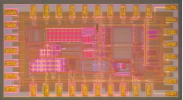
Fig. 9. Layout of the proposed controller circuit.
Fig. 10. Measured inductor current, gate signal and output voltage ripples waveforms.
output voltage at the desired level with an average efficiency of 85% for entire loading conditions.
The proposed controller IC was fabricated based on 0.13- µm HV CMOS process. The layout of the controller circuit is shown in Fig. 9. Fig. 10 shows the measured inductor current, gate signal and output voltage ripples waveforms.The output voltage ripples is within 60 mV, which is only 1 % of the output voltage.
The output voltage and power efficiency are measured in the entire output currents with 2.7V, 3 V and 3.3 V input voltages, which are shown in Fig. 11 and Fig. 12 respectively. The measured power efficiency is around 85%, which is coincided with simulation result. The measured output voltage variations change between 5.91V to 5.96 V, which is acceptable in TFT- LCD driver applications.
V. CONCLUSION
The use of a simple boost converter has been proved successfully to implement as a voltage doubler for mobile TFT-LCD display driver ICs. As shown in Fig. 7, compared with the traditional charge pump, the power efficiency of the proposed converter enhances from 70 % to 85 % at 20 mA output current.The proposed controller shows the output volt- age variations and the power efficiency are far superior to
5 10 15 20 25 30
60 65 70 75 80 85 90 95 100
Output Current (mA)
Efficiency (%)
Vin=2.7V Vin=3V Vin=3.3V
Fig. 11. Measured power efficiency in 2.7, 3 and 3.3V input voltage.
5 10 15 20 25 30
5.8 5.82 5.84 5.86 5.88 5.9 5.92 5.94 5.96 5.98 6
Output Current (mA)
Output Voltage (V)
Vin=2.7V Vin=3V Vin=3.3V
Fig. 12. Measured output voltage in 2.7, 3 and 3.3V input voltage.
the traditional charge pump design when operated in higher current applications. It also shows that the use of inductor in the design will not affect the size of the display module. As a result, the proposed circuit is a suitable replacement of the traditional charge pump circuits for future mobile TFT-LCD panels.
REFERENCES
[1] TFT LCD Driver Controller SOLOMON Systech Limited.
[2] M. J. Yim and K. W. Paik, Design and Understanding of Anisotropic Conductive Films (ACF) for LCD Packaging IEEE transactions on components, packaging, and manufacturing technology-Part a, vol. 21, no. 2, June 1998.
[3] B. Xie and H. Ding, New Challenges in Design and Understanding of Chip-On-Glass (COG) for LCD Packaging by FEA Proceedings of 2005 International Conference on Asian Green Electronics, 2005.
[4] F. Su and W. H. Ki, Component-Efficient Multiphase Switched-Capacitor DC-DC Converter With Configurable Conversion Ratios for LCD Driver Applications IEEE transactions on circuits and systems-ii: express briefs, vol. 55, no. 8, August 2008.
[5] Kyna Wong, Display Prepared for Mobile TV Display Devices, Spring, Serial no. 46, 2007.
[6] SOLOMON Systech Limited, Solomon Systech widens the series of single chip TFT LCD drivers for AV portable applications SOLOMON Systech Limited press release, 2008.
[7] SOLOMON Systech Limited, Launch of Mobile Digital TV Product Supporting China CMMB Standard SOLOMON Systech Limited press release, 2008.
[8] R. W. Erickson and D. Maksimovic, Fundamentals of Power Electronics, 2nd ed. Dordrecht, The Netherlands: Kluwer, 2001.
[9] C. C. Wang and J. C. Wu, Efficiency Improvement in Charge Pump Circuits IEEE Journal of solid-state circuits, Vol. 32, no. 6, June 1997.
[10] C. K. Tse, S. C. Wong and M. H. L. Chow, On Lossless Switched- Capacitor Power Converters IEEE Transactions on power electronics, Vol. 10, no. 3, may 1995.