國 立 交 通 大 學
電子工程學系電子研究所
博 士 論 文
可移植性數位控制式振盪器及動態頻率計數迴路之研究
The Study of Portable Digitally Controlled Oscillator and
Dynamic Frequency Counting Loop
研究生 : 陳寶龍
指導教授 : 李鎮宜 教授
可移植性數位控制式振盪器及動態頻率計數迴路之研究
The Study of Portable Digitally Controlled Oscillator and
Dynamic Frequency Counting Loop
研 究 生:陳寶龍 Student:Pao-Lung Chen
指導教授:李鎮宜 Advisor:Chen-Yi Lee
國 立 交 通 大 學
電子工程學系電子研究所
博 士 論 文
A DissertationSubmitted to Department of Electronics Engineering & Institute of Electronics College of Electrical Engineering and Computer Engineering
National Chiao Tung University in Partial Fulfillment of the Requirements
for the Degree of Doctor of Philosophy
in
Electronics Engineering November 2005
Hsinchu, Taiwan, Republic of China
可移植性數位控制式振盪器及動態頻率計數迴路之研究
研究生:陳寶龍指導教授:李鎮宜 教授
國立交通大學電子工程學系電子研究所
摘要
現代的系統單晶片(SoC)需要晶片內在的時脈產生器以及產生許多不同的頻率,來 提供給其他子系統使用,一般常用鎖相迴路為基礎的時脈產生器來達成此任務。然而, 鎖相迴路的迴路參數為了減少抖動量以及保持迴路的穩定度,因而必須依照輸出頻率以 及頻率產生倍數來調整,現有類比電路的方式需要較長的設計週期。 本論文從可移植性數位控制式振盪器,動態取樣的迴路控制器,到利用串接式迴路 來達成高倍數,提供一個實用的解決方式。具體而言,此種所提出架構的數位控制式振 盪器利用反或閘/反及閘的寄生電容差值作為數位控制式壓控變容器,不同型式的數位控 制式壓控變容器也加以討論比較。數位控制式壓控變容器能夠提升傳統標準細胞單元中 單一緩衝器的時間延遲的極限,在微調上時間解析度能夠依照使用驅動細胞單元的能力 及數位控制式壓控變容器的電容差異,作不同的選擇。同時具有較線性的時間解析度相 對於使用 OAI-AOI 細胞單元或三態緩衝器矩陣,除此之外,電路佈局圖可以利用自動 繞線及擺放的軟體工具完成。 本論文接著提出低成本的動態頻率計數迴路使用變動時間來估算及調整數位控制 式振盪器的頻率,傳統相頻器以及可程式化除頻器被數位式比較器及數位控制式振盪器 計數器取代,數位控制式振盪器計數器的值可再細分為商數向量及餘數向量,同時,使 用臨界值的設立及動態性的取樣時間來解決計數器的取樣量化問題以及提高頻率偵測 的解析度,提出的動態頻率計數迴路透過模擬比較及晶片功能驗證。本論文最後發展串接式動態頻率計數迴路應用在高倍數及低輸入頻率的應用中,所 提出的時脈產生器其倍數可從4 ~ 13888 (其中 5122 cases),其抖動量值小於輸出時脈週 期的 2.8%,最低的輸入頻率為 19.26 仟赫茲到最高輸入頻率為 60 百萬赫茲,其核心面 積為0.16 平方毫米(mm2),當工作在 1.8 伏、378 百萬赫茲時其消耗功率為 15 毫瓦,以 上所提出的設計均使用高階應體描述語言,再使用標準細胞單元件庫來合成。提出高解 析度之可移植性數位控制式振盪器、態頻率計數迴路和串接式動態頻率計數迴路在0.35 微米或0.18 微米的標準元件庫中驗證,此所提出的可移植性數位控制式振盪器、動態頻 率計數迴路和串接式動態頻率計數迴路,十分適合在系統整合的應用及系統單晶片中。
The Study of Portable Digitally Controlled Oscillator and
Dynamic Frequency Counting Loop
Student : Pao-Lung Chen Advisor : Dr. Chen-Yi Lee
Department of Electronics Engineering Institute of Electronics
National Chiao Tung University
ABSTRACT
Modern system-on-a-chip (SoC) processors often require on-chip clock generation and multiplication to produce several unrelated frequencies for other sub-systems. PLL-based clock generator is a common way of frequency multiplication to accomplish the task. However, the loop parameters must be adjusted to minimize jitter performance and insure stability for each output frequency and multiplication factors. Conventional analog skills suffer from long design cycle.
This dissertation provides a practical solution, from portable digitally controlled oscillator (DCO), dynamic sampling algorithm for loop controller, and a cascaded loop for wide multiplication range. Specifically, the proposed DCO with novel digital controlled varactors (DCV) based on parasitic capacitance difference of NOR/NAND gates can enhance the timing limitations as compared with a single buffer cell. Different types of NOR/NAND gates (2-input or 3-input) for DCV are also investigated. The timing resolution in fine-tuned stage can be decided from different driving cells and capacitance difference of each DCV cell. Thus, a high resolution DCO with better timing linearity as compared with OAI-AOI cell or
tri-state matrix is achieved. The final circuit layout can be generated using an auto placement and routing (APR) tools.
We next propose a dynamic counting loop (DFC) with low cost that uses variable time period to estimate and tune the frequency DCO. Conventional phase-frequency detector (PFD) and programmable divider are replaced with a digital arithmetic comparator and a DCO timing counter. The value in the DCO timing counter is separated into quotient and remainder vectors. Also, a threshold region is set and by using dynamic sampling period to solve the quantization effect of counter sampling and enhance resolution of frequency detection. The proposed algorithm was simulated and verified with test chips.
Finally, we develop a cascaded DFC loops that can be applied in wide multiplication ranges applications with low input frequency. The proposed clock generator achieves a multiplication ranges from 4 to 13888 (with 5122 cases) with output peak-to-peak jitter less than 2.8% of clock period. The lowest input frequency is 19.26KHz and the maximum input frequency is 60MHz. A test chip for the proposed clock generator is fabricated in 0.18 mm CMOS process with core area of 0.16 mm2. Power consumption is 15 mW @ 378 MHz with
1.8 V supply voltage. The above designs are designed in gate-level Hardware Description Language (HDL) codes and synthesized for a target cell library. The proposed portable DCO, DFC loop, and a cascaded DFC loops have been verified on silicon using 0.35-mm or 0.18-mm CMOS cell library. As a result, the proposed portable DCO, DFC loop and cascaded DFC loops are well-suited for system-level integration and SoC applications.
Acknowledgments
I would like to express my deepest gratitude to my advisor Prof. Chen-Yi Lee for his sophomore enthusiastic guidance and encouragement throughout the research, and wholeheartedly give him and his family my best wishes. I also appreciate professor Wei Hwang, professor Shen-Iuan Liu, professor Shyh-Jye Jou, professor Jin-Shyan Wang, Professor An-Yeu Wu, professor Ching-Yuan Yang and professor Terng-Yin Hsu for their fruitful opinions.
During my research, I would like to thanks National Science Councile (NSC) for supporting the project of my Ph.D work. The chip support from Chip Implementation Center (CIC) of NSC is acknowledged, too.
I want to thank my senior Si2 group mate, Dr. Ching-Che, Chung for many valuable discussions and great help. Besides, I want to thank all members of the Si2 group of NCTU for plenty of fruitful assistance. I also want to appreciate the friends for fruitful e-mail discussions with their published papers.
Finally, I give greatest respect and love to my family and my wife, and I want to express my highest appreciation for their support and understanding.
誌
謝
在這六年半的博士生涯中,首先我要向指導教授李鎮宜博士表達最誠摯的謝意。由 於老師指導有方,讓我能在短時間內找到正確的研究方向;在遇到挫折時也能從經驗中 學習,培養正確的研究精神。而在論文定稿之前,感謝口試委員黃威教授、劉深淵教授、 周世傑教授、王進賢教授、吳安宇教授、楊清淵教授、許騰尹教授提供寶貴的意見、使 論文得以完成。同時我要感謝國科會及國家晶片中心,另外,我也要感謝Si2 實驗室中 的每一位成員。在這裡的每個人研究領域或有不同,但都願意彼此幫助,讓我不僅了解 團隊工作的重要性,更令人倍感溫馨;尤其我要感謝鍾菁哲學長,在我研究過程中不厭 其煩地提供不少建議及幫忙。除此之外,我也要感謝那些未曾謀面的前輩們,透過e-mail 不厭其煩地回答我關於他們所發表的論文。最後,我要謝謝父母親及與在背後默默支持 著我的太太瑞蓮、家人和朋友,讓我順利完成了這份學業。在大家的鼓勵下,讓我過得 更多采多姿,我一定不會忘記這段令人充滿回憶的生活。最後謹將本篇論文獻給所有曾 經對我的博士論文有過幫助或關心的人。
Contents
Chapter 1 Introduction 1 1.1 Thesis Background 1 1.2 Thesis Motivation 2 1.3 Thesis Contribution 4 1.4 Thesis Organization 6Chapter 2 Overview of Clock Generator with Phase Locked Loop 7
2.1 PLL Basics 7
2.1.1 Analog PLL 8
2.1.2 Charge Pump PLL 11
2.2 All-Digital PLL 12
2.2.1 DCO with Fixed High-speed Clock 12 2.2.2 Direct DCO Synthesis Clock 14 2.2.3 Standard Cell-Based DCO 15 2.3 Design Trade-off of Clock Generator with Different PLLs 17
Chapter 3 Digitally Controlled Oscillator with Novel Varactor 22
3.1 Basic Concept of Digitally Controlled Oscillator 22 3.1.1 Basic DCO Design Approach 23 3.1.2 Enhance Fine Resolution of DCO design 25 3.1.3 Fine Tune in Standard Cell Library 27 3.2 Digitally Controlled Oscillator with DCVs 29 3.2.1 Digitally Controlled Varactors 30
3.2.2 Performance of the Digitally Controlled Varactors 33 3.3 Structure of Proposed DCO 34
3.3.1 Structure of DCO 34
3.3.2 Design of DCVs 36
3.3.3 Laboratory Test Result 37 3.3.4 Porting DCO to different processes 38
3.4 Summary 40
Chapter 4 Dynamic Frequency Counting Loop for All-Digital Clock Generator
41
4.1 Introduction 41
4.2 Algorithm and Structure of Dynamic Frequency Counting Loop 43 4.2.1 Algorithm of Dynamic Frequency Counting 42 4.2.2 Structure of Reference and DCO Timing Counter 48 4.2.3 Structure of DFC Loop Counter 50 4.3 Analysis of Proposed Algorithm 52 4.3.1 Error of Frequency Detection 52 4.3.2 Jitter Variation and Threshold Decision 52
4.4 Simulations 54
4.5 Experimental Results 56
4.6 Summary 60
Chapter 5 Clock Generation with Cascaded DFC Loops for Wide Multiplication Range Applications
61
5.1 Introduction 62
5.2 System Block and Loop Parameter Design 65 5.2.1 Issues in DFC Loop When Multiplication N is large 65
5.2.2 Cascaded DFC Loops 66 5.3 Design of DCOs for Cascaded DFC Loops 68 5.3.1 Structure of DCO1 68 5.3.2 High Resolution DCO2 with Digitally Controlled Varactors 70 5.4 Experimental Results 71
5.5 Summary 77
Chapter 6 Conclusions and Future Works 79
6.1 Conclusions 79
6.2 Future Works 81
References 82
VITA 89
List of Figures
Figure 1.1 SoC Media Networking Processor [24]……….. 4
Figure 2.1 Block diagram of an analog PLL……… 8
Figure 2.2 (a) Three state phase frequency detector. (b) State transition of PFD…… 9
Figure 2.3 A first order loop filter with RC implementation………... 10
Figure 2.4 Magnitude response of a second order loop transfer function………….... 10
Figure 2.5 Block diagram of a charge pump PLL………... 11
Figure 2.6 ADPLL with fixed high-speed clock to form DCO in [3]……….. 12
Figure 2.7 Z-plane representation of the loop………...………. 14
Figure 2.8 ADPLL with direct DCO synthesis clock in [37]..……… 14
Figure 2.9 Functional block of ADPLL in [50]………... 16
Figure 2.10 Signal block diagram of standard cell-based all-digital PLL………. 16
Figure 2.11 PLL frequency synthesizer with DPFD [62]. (a) Functional block diagram. (b) Structure of DPFD. 18 Figure 2.12 Hybrid PLL frequency synthesizer with DLT table [70]……… 19
Figure 2.13 Time-to-Digital conversion circuit [51]……….. 20
Figure 3.1 DCO constructed with DAC and VCO (ICO)……… 23
Figure 3.2 DCO constructed with high-speed clock and divider………. 24
Figure 3.3 DCO constructed with variable length ring oscillator……… 24
Figure 3.4 General mechanism for enhance of fine tune in DCO……… 25 Figure 3.5 DCO with fine resolution constructed with current starved ring oscillator 25
Figure 3.6 DCO with differential capacitance for fine resolution (a). Circuit structure. (b). Gate capacitance v.s. gate voltage for PMOS varactor (L=0.5 mm, W=0.6 mm).
26
Figure 3.7 DCO with tri-buffer matrix……… 27
Figure 3.8 DCO with AOI-OAI as fine tuning……….. 28
Figure 3.9 Fine tune of DCO with delay difference……… 28
Figure 3.10 (a). Delay control in [71]. (b). Delay control in [56].………. 29
Figure 3.11 Conventional digitally-controlled mechanism with shunt capacitor…….. 30
Figure 3.12 Proposed DCV with two-input NOR gate. (a) Circuit with digital control. (b) Equivalent circuit with ΔC capacitance. 30 Figure 3.13 Variation of two-input NOR gate’s capacitance when D=0 and D=1…… 31
Figure 3.14 Three different types of DCV cell.(a) Two-input NAND, (b) Three-input NOR, (c) Three-input NAND. 32 Figure 3.15 Comparisons among the proposed DCV and other approaches…………. 33
Figure 3.16 The proposed DCV using two-input NOR under different PVT conditions. 34 Figure 3.17 Proposed digitally controlled oscillator with DCV in the fine-tuning stage. 35 Figure 3.18 Microphotograph of DCO test chip……… 37
Figure 3.19 Chip measured results compared to linear Eq. (3.7) under 3.3V/25 0C….. 38
Figure 3.20 Circuit simulation with DCO 15-bit under different process (typical, 25 0C). 40 Figure 4.1 Functional block diagram of [41]……… 42
Figure 4.2 The loop control algorithm for proposed DFC loop……….. 44
Figure 4.4 Basic structure of dynamic frequency counting loop………. 46 Figure 4.5 Signal model of the proposed dynamic frequency counting loop……….. 46 Figure 4.6 Pole displacement by gain variation………... 47 Figure 4.7 Step response of the proposed clock generator with DFC loop control
v.s. sequential search (a). Proposed. (b). Sequential search. (c). Jitter variation.
48
Figure 4.8 Structure of quotient and remainder vectors in the DCO timing counter... 49 Figure 4.9 Structure of the proposed DFC loop controller……….. 50 Figure 4.10 State transition of the proposed DFC loop controller (a). State of
frequency search. (b). State of sampling period.
51
Figure 4.11 Verilog simulation of the proposed DFC loop control, input clock=1 MHz, N=127.
54
Figure 4.12 Proposed DFC loop V.S. fixed sampling clock = 8, when N=2, input clock at 20MHz.
55
Figure 4.13 Proposed DFC loop with reference clock at 10MHz with peak-to-peak jitter 27% over clock period and N=10, output frequency at 100MHz with peak-to-peak jitter 8.96% over output clock period.
56
Figure 4.14(a)
Measured result with multiplication factor N=48, reference clock =
1MHz with peak-to-peak jitter 260 ps, and test output=24.07MHz with peak-to-peak jitter 70ps (DCO output at 48.14MHz).
57
Figure 4.14(b)
Measured result with multiplication factor N=192, reference clock = 250
KHz with peak-to-peak jitter 300ps, and test output=24.02MHz with peak-to-peak jitter 60ps (DCO output at 48.04MHz).
Figure 4.15 Measured result with multiplication factor N=128, reference clock = 2.4 MHz with peak-to-peak jitter 220ps, and test output=153.9MHz with peak-to-peak jitter 70ps (DCO output at 307.8MHz).
58
Figure 4.16 Measured average frequency error v.s. calculated by Eq.(4.12) (output test 24MHz, internal DCO at 24MHz x 2 = 48MHz).
58
Figure 5.1 A CP-PLL clock generator with programmable 1/N current mirror [11]... 63 Figure 5.2 Structure of programmable 1/N current mirror in [11]………... 64 Figure 5.3 Structure of proposed clock generator with cascaded DFC loops……….. 67 Figure 5.4 Structure of DCO 1………. 69 Figure 5.5 Using three-input NAND gate as DCV. (a) Circuit with digital control.
(b) Equivalent circuit with ΔC capacitance.
70
Figure 5.6 256 DCVs in the fine-tuning stage of DCO 2………. 70 Figure 5.7 (a) Simulation result with (N=320), N1=40, N2=8, CKref=500KHz, and
output=160 MHz. (b) Simulation result with (N=12800), N1=200, N2=64, CKref=10KHz, and output=128 MHz.
72
Figure 5.8 Measured results with N=13888 (N1=224, N2=62), REF_clk=19.26KHz. (a) DCO 1 output @ 4.30 MHz with peak-to-peak jitter 110ps . (b). DCO 2 test output @ 134.7 MHz with peak-to-peak jitter 200 ps (DCO 2 output at 269.4MHz).
74
Figure 5.9 Measured output cycle-to-cycle jitter V.S. multiplication factor (N) for fixed input clock=19.26KHz and fixed output clock=134.7MHz (internal DCO at 269.4 MHz).
75
Figure 5.10 Microphotograph of the proposed clock generator with cascaded DFC loops.
List of Tables
Table 3.1 Comparisons among different types of proposed DCV cells………. 32
Table 3.2 Comparisons with existing DCOs……….. 38
Table 3.3 Resolution of Tbuffer and Tfine……….. 39
Table 3.4 DCO output frequency range for different processes under typical
condition.
39
Table 4.1 Fixed sampling period V.S. locked cycle period……… 55
Table 4.2 Simulations with different input frequencies and multiplication factors 56
Table 5.1 Summary of chip features of cascaded DFC loops………. 76
Chapter 1
Introduction
1.1 Thesis Background
Traditionally, phase locked loops (PLL) based clock generators for microprocessor are the common way of frequency multiplication from a low-frequency reference clock, typically from quartz oscillator [1-13]. As VLSI technology grows up rapidly, the advance of semiconductor process enables the successful realization of system-on-a-chip (SoC) [14-17,21,23-24]. Modern SoC processors integrate both analog and digital real-time functions, such as a digital signal processor (DSP), digital-to-analog converter (DAC), audio, video, and I/O interface protocols. An off-chip clock costs power to generate and to distribute on the PC-board. In addition, the ability to oscillate at different frequencies reduces costs by eliminating the need for additional oscillators to a system. Such applications often require on-chip clock generation and multiplication to produce several unrelated frequencies for digital signal processing, I/O interfaces, as well as sampled analog sub-systems [18-19].
One solution is to create one PLL-based clock generator running at a high frequency that can then be divided down to obtain all the desired frequencies [20]. The disadvantage of this approach is the high power consumption and stringent jitter requirements. Another approach is to have a dedicated PLL for each clock domain [21]. This solution is very costly in term of power and area.
multiplication factors required from PLLs. The loop parameters must be adjusted to minimize jitter performance and to insure stability for each PLL output frequency and multiplication factors. Providing ample flexibility for a variety of applications is a big challenge for PLL design. The design of PLL-based clock generator is a trade-off among jitter performance, frequency/phase resolution, lock-in time, power consumption, area-cost, circuit complexity and design time. It often needs to redesign the PLL for target applications. If a wide-range PLL is designed for SoC applications, it can be used in more modules without modify it. However, this scheme may waste unnecessary area cost and power consumption due to the requirement of wide-range operation. Thus, it is a challenge task to design it based on conventional analog skill.
In addition, most PLL design use mixed signal and full custom design techniques, which can not be fully integrated in digital environment. Due to time-to-market issue, the design cycle remains the same or even shorter. Thus in System-on-a-Chip (SoC) designs [22], each module had better to be reusable and process portable, so that the total design time can be reduced. As a result, how to design a synthesizer clock generator in an efficient way becomes more important.
1.2 Thesis Motivation
The all-digital PLLs have several advantages over their analog counterparts. Firstly, traditional analog loop filter costs a lot of chip areas. Using digital loop filters gives benefits such as robustness against noise, and also the ability to design higher order filters without much extra power consumption and area penalty. Secondly, analog component are vulnerable to DC offset and drift phenomena that are not present in equivalent digital implementations [35]. Furthermore, the loop dynamics of analog PLLs are quite sensitive to process technology scaling, whereas the behavior of digital logic remains unchanged with scaling; this
requires much more significant redesign effort to migrate analog PLLs to a new technology node than is required for all-digital PLLs.
Moreover, power consumption is extreme concern for portable, battery-powered, computing system, as power dissipation relates directly to battery life. As a result, many manufactures are reducing the power supply voltage requirements of the integrated circuits, particularly those that are especially adapted for portable computing system [36]. However, reduction in power supply voltage applied to analog circuitry, such as analog and digital PLLs, does not reduce the power dissipated by these circuits. Additionally, reduction in power supply voltage to analog circuits renders the design of robust circuit much more difficult.
For these reason, PLLs in which digital techniques are used in not only the phase detector, but also in the loop filter and the controllable oscillator, are very attractive to designers. All-digital cell-based approach is preferred for SoC applications [44-50]. It can reduce significantly both design time and design complexity by using Verilog (or VHDL) hardware-description language and the final circuit layout to be generated by using an auto placement and routing (APR) tools.
A production SoC with high-performance audio/video media networking processor as shown in Fig 1.1 has successfully applied four standard cell-based digitally controlled oscillators (DCO) [57] to replace two external analog audio PLLs and two external quartz oscillators [23-24]. By saving two external analog PLLs, 4 I/O pins (2 per PLL) are saved. Another two I/O pins for connecting quartz oscillators are also reduced. However, due to the limitations of standard cell-based design, it is difficult to achieve a low jitter, low-power, and high resolution all-digital cell-based clock generator [45-50,57]. Thus, how to overcome the limitations of standard cells to build up a high resolution DCO with better linearity and less power consumption, and propose new control algorithm for clock generator are the important design challenges for our research.
Fig. 1.1 SoC Media Networking Processor [24].
1.3 Thesis Contribution
In this dissertation, we address the issue of portable digitally controlled oscillator (DCO) and propose dynamic sampling period algorithm to enhance frequency detection. In addition, a cascade dynamic frequency counting loops for wide multiplication application is developed. The contributions are listed as follows:
n Portable Digitally Controlled Oscillator with Novel Varactors
In this thesis, we first present a portable digitally controlled oscillator (DCO) by using two-input NOR gates as a digitally controlled varactor (DCV) in fine-tuning delay cell design.
This novel varactor uses the parasitic capacitances difference of NOR gates under different digital control inputs to establish a digitally controlled varactor. Thus proposed DCO can improve delay resolution 256 times better than a single buffer design. This study also examines different types of NOR/NAND gates (2-input or 3-input) for DCV. The final circuit layout can be generated using an auto placement and routing (APR) tools. A test chip demonstrates that LSB resolution of the DCO can be improved to averaged 1.55 ps with standard 0.35-mm 2P4M CMOS digital cell library. The proposed DCO has good performance in terms of fine resolution, testability, and short design turn-around cycle compared with conventional DCO designs.
n A New Algorithm with Dynamic Frequency Counting Loop
Second, a new algorithm with dynamic frequency counting (DFC) that multiplying input reference frequency by N times is presented. The DFC loop which uses variable time period to estimate and tune the frequency of digitally controlled oscillator (DCO) enhances the resolution of frequency detection. One up counter serves as variable timer and another DCO timing counter acts as frequency estimator. Conventional phase-frequency detector (PFD) thus is replaced with a digital arithmetic comparator to yield a simple circuit structure. The proposed algorithm was simulated and compared with other method. Then, the performances were measured from 0.35-mm and 0.18-um chips.
n Cascaded DFC Loops for Wide Range Multiplication Applications
Finally, a clock generator with cascaded dynamic frequency counting (DFC) loops for wide multiplication range applications is presented. The loop stability can be retained by cascading two DFC loops when multiplication factor (N) is large. The design complexity is tremendously reduced without using the analog component. The proposed clock generator is fabricated in 0.18-mm CMOS process with core area of 0.16mm2. Experimental results of the
clock generator are given in this chapter.
1.4 Thesis Organization
The organization of this thesis is as follows: In chapter 1, we introduce that different clock domains are required in a SoC chip. Using portable clock generator to replace conventional PLL is feasible. For the rest of this dissertation is organized as follows.
In chapter 2, we give an overview of PLL related techniques for clock generator. Properties of analog, digital PLL as well as charge-pump PLL are addressed. Then, all-digital PLL with different DCO approaches are discussed. The design trade-off of clock generator with different PLL architecture is also investigated.
In chapter 3, we first introduce the fundamentals of digitally controlled oscillator. We also introduce different approaches to enhance the fine tune solution of DCO. Then, we focus on the operation of digitally controlled varactors with two-input or three-input NOR/NAND gates designs. Then, we apply the DCV as fine tune cell to build high resolution digitally controlled oscillator. A detailed description of the circuits and experimental results are given.
In chapter 4, we describe a dynamic sampling technique to enhance the resolution of frequency detection by using simple structure. Detailed algorithm and structure of the loop are then discussed. Then, the proposed algorithm was verified in 0.35-um and 0.18-um.
In chapter 5, we utilize the dynamic sampling techniques for wide range multiplication applications by cascade loops. The multiplication factors range from 4 to 13888 (224 x 62). The peak-to-peak jitter is less than 2.8% of output clock period. Then, we talk how to design the DCO in each loop as well as the loop parameters. Finally, we discuss the experiment results and the overflow issue.
In chapter 6, some concluding remarks will be derived from this research. Finally, we describe several design issues that needed to be further explored in the near future.
Chapter 2
Overview of Clock Generators with
Phase Locked Loop (PLL)
As shown in chapter 1, numerous applications, such as video graphics card, microprocessor and telecommunication system, require a clock synthesizer. Quartz oscillators frequently require conversion when operating at low frequency. Several methods exist for realizing frequency multiplication: phase locked loop (PLL) [1-13], delay locked loop (DLL) [25-32], and direct digital synthesis (DDS) in [33]. The basic concept of DLL is similar with PLL. The major difference is the voltage controlled delay line (VCDL) in DLL and voltage controlled oscillator (VCO) in PLL [68]. Each of these methods has advantages and disadvantages for frequency multiplication. DLL approach may offer better jitter performance than PLL approach because the noise induced by the power supply or substrate noise disappears at the end of the delay line. However, DLL-based method is not suitable for wide multiplication range applications. The direct digital synthesis (DDS) in [33] applied accumulator and D/A converter mechanism for frequency synthesis. Therefore, we only focus on the PLL approach in this work.
The organization of this chapter is as follows. Section 2.1 describes the preliminary knowledge of analog PLL and charge pump PLL. Basics of all-digital PLL and standard cell-based approach are discussed in section 2.2. Design trade-off in different PLL architecture is discussed in section 2.3.
2.1 PLL Basics
PLL-based clock generator has been widely used in the industry. In addition, PLL-based approach is the most suitable for integrating into a standard CMOS process. Phase-locked loops are originally of analog nature [1-3]. The operation principle is summarized in this section and the steps towards charge pump PLL are described in the subsequent sections.
2.1.1 Analog PLL
The PLL’s characteristics are determined by the characteristics of phase detector, voltage controlled oscillator and low pass filter. In [1-3] indicated two factors will influence the performance, one is the phase error – the difference between the input phase and output phase, and another is the frequency range – what range over which it will acquire lock. As a result, PLL can be regarded as a tracking phase system. An analog PLL consist of the three main building blocks as shown in Fig. 2.1.
Fig. 2.1. Block diagram of an analog PLL.
l Phase detector: It compares the phase of the input signal (reference signal) with the phase of the feedback signal. The output of the PD is ideally proportional to the phase difference θe .
UD(s) = KD (θi(s) - θo(s))= KD θe(s) (2.1)
where KD is the phase detector gain in [V/rad] and θi and θo are the phase of the input
and output signals respectively. If the analog phase detector like multiplier is replaced with three-state phase frequency detector (PFD) as shown in Fig. 2.2 (a), then it is defined as digital PLL in [3]. Fig. 2.2 (b) illustrates the PFD state diagram including
Down, Zero, and Up states. The PFD detects not only the phase difference but also the frequency difference between its two inputs. During the phase-locking process the relative time that the PFD remains in `Down' or `Up' state represents the phase error. If the PLL is locked, the output of ‘QA’ and ‘QB’ are activated only during extremely short
time spans. However, the practical PFD circuit suffers from the dead-zone problem [3].
D CK Q D CK Q VDD VDD CKref CKfb Reset QA QB QA=1 QB=0 Up QA=0 QB=0 Zero QA=0 QB=1 Down CKref CKfb CKref CKfb
Fig. 2.2. (a) Three state phase frequency detector. (b) PFD state diagram.
l Voltage controlled oscillator (VCO): Translates the filter output into a frequency. Due to the transformation of phase information into a frequency, it has the characteristic of an integrator with gain K0 [rad/sV].
θo(s) = s K s UO( )× o . (2.2) l _ Low pass filter (LPF) : Filters the output voltage of the phase detector with the transfer
function F(s) can be expressed in
Uo(s) = UD(s)F(s). (2.3)
The loop filter reduces the AC loop gain and the loop bandwidth to remove the frequency that we do not want in the loop. The overall transfer function of the closed loop becomes
H(s) = ) ( ) ( s s i o q q = ) ( ) ( s F K K s s F K K o D o D + . (2.4)
R1
R2 C
UD Uo
Fig. 2.3. A first order loop filter with RC implementation.
The characteristics of the LPF are important which they determines lot of parameters of the loop. Three parameters for engineer to choice: (1) the loop gain, (2) the placement of the zeros, and (3) the placement of the poles that we need. A first order loop filter is depicted in Fig. 2.2 that has the following transfer function:
F(s)= ) ( 1 1 2 1 2 C R C R s C sR + + + . (2.5)
The overall loop transfer function is a second order loop with low-pass characteristic. The natural frequency is
ω
n=
C R C R K KD O 2 1 + (2.6) and the damping factor becomesζ = ( 1 ) 2 2 D O n K K C R + w . (2.7) A PLL uses a first order loop filter is therefore a second order system. Figure 2.4 shows the transfer functions of a second order loop for various damping factors ζ .
2.1.2 Charge Pump PLL
To trade-offs between ζ,
ω
n, and the phase error, the analog/digital PLLs suffer from a critical drawback: limited acquisition range. A charge pump (CP) PLL was proposed in [34] to solve this problem as shown in Fig. 2.5. A charge pump consists of two switched current sources that pump charge into or out of the loop filter according to two logical inputs. The three state PFD detects phase or frequency differences, and activates the charge pump accordingly. The gain of PFD/CP combination is infinite, which can not achieved by the digital PLL. When in lock, the PLL generates the output frequency that is N times the reference frequency. The system is second order closed loop response because the integration of charge on the loop filter and the integration of phase.Voltage-controlled oscillator (VCO) CKref + -CKout U qo qi Frequency Divider N qb D Icp R C Charge Pump Loop Filter Icp PFD KPFD Uo(s) KVCO/s UPFD(s) F(s)
Fig. 2.5. Block diagram of a charge pump PLL.
The loop bandwidth (rad/s) of a CP-PLL is given by
ω
n=
I2CPp××NKVCO×C (2.8) and the damping factor can be described inζ = ×ωn×R×C
2 1
The loop bandwidth characterizes the response rate of the system and the damping factor characterizes its stability. Ideally,
ω
nshould scale with the CKref to handle a wide frequencyrange. However, the
ω
n is influenced by the divider ratio as indicated in (2.8). This creates achallenge for PLL with wide range N.
2.2 All-Digital PLL
The all-digital phase lock loop (ADPLL) has gained increased attention in recent years. All analog building blocks are replaced with digital representations in all-digital PLLs (ADPLL). The term “all-digital PLL” is used for a particular reasons: all signals within this PLL are digital values; no analog level is used. Many different ADPLL are discussed in the literature [69]. In general, there are two types of ADPLL depending on the DCO clock source: (1) to use fixed high-speed clock as indicated in [2,15,43,57] to form a DCO, (2) to synthesis clock internal based on a DCO circuit as [37-39, 42]. Furthermore, the standard cell-based implementation of DCO will also be discussed because of its popularity [50].
2.2.1 DCO with Fixed High-Speed Clock
Fig. 2.6 shows the proposed ADPLL with fixed high-speed clock and output accumulator in [3].
Register AccumulatorOutput
fclock Noffset X2 fin N2 N2 Nout -q
The input is a binary fin, and the output is to be a number that has an average repetition
rate of fin but follows the input with a closeness that depends on the loop parameters. The
DCO consists of an accumulator and high speed clock fclock. Its output is a number that
changes each clock cycle by an amount equal to its input N2. Each time the output
accumulator reaches its capacity Nmax, it recycles to 0. Thus, one cycle is represented by Nmax,
and the output phase of the output accumulator is
Φout = (Nout /Nmax) cycles (2.10)
The output frequency is
fout = ΔΦout / Δt = (N2 / Nmax).fclock (2.11)
since the output is incremented by N2 each cycle of the output accumulator. The register
stores the value of Nout at each cycle of the input signal fin. The register thus functions as a
phase detector and zero-order hold. Then, the phase error will be inversed and multiply with 2-q. There are two sampling processes occurring in the simple loop, one in the register at f
in
and one in the output accumulator at fclock. The stability of this simple loop can be represented
by using z-transform. The closed loop of Fig. 2.6 is
H(z) = K z K + -1 , (2.12) where K = 2-q (f clock / fin). (2.13)
The open and closed loop poles for this loop are shown Fig. The closed loop pole locus begins at the open loop pole when K=0 and moves along the real axis as K increases. The beset response will be in the center of the unit circle where K=1. The closed loop is unstable when K is larger than 2.
Fig. 2.7. Z-plane representation of the loop [3].
2.2.2 Direct DCO Synthesis Clock
If the high-speed clock is available, such as in SoC, and the target operation’s speed is not very high, then DCO with fixed high-speed clock can be the choice. However, it may consume large power due to high-speed clock operation. The external high-speed clock is not always feasible which require extra pin and another high-speed quartz oscillator when the target application is for on-chip clock multiplication (factor > 1). In recent years, ADPLL of type (2) is more popular and even applied frequency synthesis for RF wireless application [40-41,54]. An ADPLL with high resolution DCO as shown in Fig. 2.8 was first proposed in [37] as clock generator for microprocessor that did not require external fixed high-speed clock as compared with Fig. 2.6.
This ADPLL achieved fast locking within 50 reference clock cycles as compared with conventional charge pump PLL-based clock generator. The fast locking time was achieved with modified binary searching algorithm. It separated the frequency acquisition and phase acquisition that did not utilize the three-state PFD and frequency divider. A high-resolution frequency comparator with matching delay line was utilized to achieve frequency accuracy under 0.1% error ratio. A high-resolution ring oscillator with 16-bit control word was implemented to generate the accurate frequency output. The DCO will be turn-on and disable after 30-40 iterations for frequency comparison. An anchor register is needed to store the baseline frequency. After frequency acquisition is completed, the PLL starts to trace the phase of the reference clock. The phase tracking process was performed with a phase control algorithm and a phase detector. It contains phase gain controller and two series-connected, edge-triggered D flip-flops. The phase acquisition process can be finished within 10 reference clock cycles. After the frequency acquisition and phase acquisition, the ADPLL enters phase and frequency tracking process. Many ADPLL variants follow this ADPLL approach, such as [38-39]. However, the cost of this chip area is extremely high due to DCO. Another small area DCO was proposed in [38]. Those DCO designs were required to be with full-custom layout. The specific transistor sizing of DCO comes to be with changes in design specifications.
2.2.3 Standard Cell-Based DCO
A standard cell-based implementation of all-digital clock generator [50] based on structure of digital PLL that can be divided into five main parts: PFD, loop controller, loop filter, DCO, and programmable divider as shown in Fig 2.9. The key issue is that all of the elements are designed form standard cell library without any fully-custom layout.
Fig. 2.9. Functional block of ADPLL in [50].
The function of the programmable divider is simply to slow the DCO output frequency for comparison. The loop controller generates the digital commands to track the DCO output clock based on the results from PFD. Two extra digital pulse amplifier circuits are required to minimize the dead zone of PFD, as indicated in [50]. However, the control code may have small variations due to the following factors: PFD’s dead zone, DCO’s finite resolution. An average loop filter is necessary to filter out the rippling and produce a smoother digital controlled word with less jumping. Additionally, two DCOs are required for low output jitter to reduce the noise and jitter associated with input reference. This requirement leads to a highly complex and expensive design. Therefore, this structure was effectively creating a frequency locked loop. The cell-based ADPLL of Fig. 2.9 can be modeled as shown in Fig. 2.10.
PFD KD Digital filter Digitally controlled oscillator KO D(z) CKref F(z) + -CKout UD UO qo qi Frequency Divider N qb
The closed-loop transfer function of Fig. 2.10 is H(z)= ) ( ) ( z z i o q q = ) ( ) ( ) ( ) ( z D z F K K N z D z F K K N O D O D × × × + × × × × (2.12)
The stability of the closed loop transfer function depending on KD, KO, N and F(z). Different
types of loop filter are discussed in [49].
2.3 Clock Generator Trade-off with Different PLL
Architectures
PLL-based clock generator is a trade-off lock-in time, area cost, power consumption, jitter performance, circuit complexity and design time. Thus, it is very challenge to design one PLL clock generator for all applications. The conventional charge pump PLL-based clock generators for microprocessor as indicated [6,8-10] that can accomplish good jitter performance as well as low power consumption. However, the on-chip loop filter occupied a lot of chip area and slow lock-in time. Furthermore, it required long design time due to circuit complexity. Therefore, those clock generators are also only suitable specific application which can not be applied a variety of multiplication ranges. In order to handle wide multiplication range, Ref. [11] utilized a scalable charge-pump current to compensate for the damping factor and bandwidth dependence of the multiplication factor. The multiplication factor (N) of [11] can range from 1 to 4096. However the proposed architecture leads to design complexity and also has large die area due to the 12-bit programmable 1/N current mirror.
In conventional PLL-based clock generator design, fast acquisition requires tuning the free-running frequency near the desired frequency in advance or to increase the loop bandwidth. The exact VCO tuning range is not easy to be achieved since there always has
process variations, voltage variation, and temperature variations (PVT variations). A Discriminator-Aided Phase Detector (DAPD) in [64] can be applied to reduce the PLL pull-in time and enhance the switching speed. This makes the charge pump circuits more complex, and the loop filter is off-chip.
A Digital Phase-Frequency Detector (DPFD) as indicated in Fig. 2.11 is proposed in [62] to convert the frequency directly to the digital value, and then change the gain for VCO control adaptively. It required a complex D/A converter that occupied a lot of chip area and power consumption. A different way to achieve fast-lock is proposed in [70] as shown in Fig. 2.12. It uses a digital hybrid PLL with Digital Look-up Table (DLT) to directly adjust VCO output to the desired frequency, and the use a traditional analog PLL to fine-tune the output frequency. However, this digital look-up table is still dependent on PVT variations. As a result, acquisition time increases in proportion to the initial frequency difference.
(b)
Fig. 2.11. PLL frequency synthesizer with DPFD [62]. (a) Functional block diagram. (b) Structure of DPFD. VCO CKref + -CKout Programmable Counter Phase Detector S Charge Pump Loop Filter D/A Digital Look-up Table Frequency Control Word + +
Fig. 2.12. Hybrid PLL frequency synthesizer with DLT table [70].
To further speed up lock time, a Time-to-Digital (TDC) circuit as shown in Fig. 2.13 can be used to quantize the reference clock period ratio into multiple of inverter delay times as indicated in [51]. This all-digital PLL replaces the DLT with TDC to against PVT variations and speed up the frequency acquisition process. However, the area cost for the TDC processing unit is large if a small chip area is required.
Fig. 2.13. Time-to-Digital conversion circuit [51].
An all-digital PLL as indicated in section 2.2.2 that uses the modified binary search which can achieves 50 cycles lock-in time for clock multiplier applications (multiplication factor: 4). This ADPLL can keep tracking the phase of the reference clock by using an anchor register to store the baseline frequency and a complex phase/frequency tracking algorithm. The phase error of this ADPLL may become worst when multiplication ratio is increased. In addition, its DCO needs to be full-custom design, making it difficult for porting to different process as design specification to be changed.
Thus, efforts at the physical design level remain unsolved. A complete clock generator
design using standard cell only as the IP block with portability in [44-50] can partially solve the problem. A portable clock multiplier generator using digital CMOS standard cells based is presented in [44]. However, its multiplication factor is limited to 4~20. Additionally, three large register files are required for storing the history of previous 256 cycles. The chip area also is very big and dependent on multiplication factor.
The standard cell-based DCO with delay matrix architecture to improve the resolution in the fine-tuning is developed in [47-48]. But, the proposed fine-search delay matrix also occupies large silicon area and high power consumption. Also, two DCOs are required to
reduce the output clock jitter effectively. From the above discussions, a better DCO with high resolution and a new loop control algorithm has to be explored for different SoC and low cost applications.
Chapter 3
Digitally Controlled Oscillator with
Novel Varactors
Traditional analog circuit design, such as voltage-controlled oscillator (VCO), shifts the design paradigm towards more digitally-intensive techniques, easier testability and less parameter variability because of process migration. Digitally controlled oscillator is the key component of all-digital PLL. Thus, this chapter attempts to propose a high resolution DCO by using NOR/NAND gates as novel varactor.
The organization of this chapter is as follows. Section 3.1 describes the preliminary concept of DCO, basic DCO design and fine tune methods. The novel digital controlled varactor is discussed in section 3.2. Section 3.3 describes the structure of DCO. Summary is in section 3.4.
3.1
Basic Concepts of Digitally Controlled Oscillator
The fundamental function of a DCO is to provide an output waveform, typically in the form of square wave, which has a frequency of oscillation
f
DCO that is a function of a digitalinput word D, as follows:
f
DCO =f
(D) =f
( dn-1 2n-1 + dn-2 2n-2 + ···+ d1 21+d0 20). (3.1)Typically, the DCO transfer function
f
(···) is defined so that either the frequencyf
DCO or theperiod of oscillation TDCO is linear with D, generally with an offset. For example, a DCO
f
(D)=f
offset + D ·Δf
(3.2)where foffset is a constant offset frequency and Δ
f
is the frequency quantization step. Similarly,a DCO transfer function that is linear in period is typically expressed as:
T(D)= 1/
f
(D)=Toffset + D ·ΔT (3.3)where Toffset is constant offset period and ΔT is the period quantization step. It is evident that,
since the DCO period T(D) is a function of quantized digital input D, the DCO can not generate a continuous range of frequencies. In this regard, the quantization granularity of the DCO period sets some fundamental limits on the achievable jitter of an all-digital PLL. It is of course desirable to have a fairly small quantization step size (e.g. period quantization step ΔT).
3.1.1 Basic DCO Design Approaches
One simple method to implement DCO in [53] is directly utilized digital-to-analog (DAC) converter and conventional voltage (current) controlled oscillator (VCO, ICO) as shown in Fig. 3.1. However, to design a high resolution DAC (e.g. 16 bits) is extremely difficult. In addition,the VCO is an analog block that is easy to be influence by power and substrate noise. It also requires extensive design efforts when specifications are changed or transfer into other technology processes. The chip area cost is very high due to DAC and VCO.
Digital in DAC VCO (ICO)
Fig. 3.1. DCO constructed with DAC and VCO (ICO).
Another common type of conventional DCO includes a high frequency oscillator in combination with a programmable frequency divider. Figure 3.2 shows the DCO. A
programmable frequency divider receives an n-bit digital control word D which indicates the divisor values. The output DCO (CLK) signal is to be divided from a high speed oscillator (HFCLK). Programmable Frequency Divider n D HFCLK CLK
Fig. 3.2. DCO constructed with high-speed clock and divider.
The period quantization step ΔT is limited by the high frequency oscillator (HFCLK) in this arrangement. Low jitter operation thus requires oscillator to operate at an extremely high frequency; for example, a 100 ps step between periods require high frequency oscillator and programmable counter to operate at 10 GHz. This will consume a lot of power consumption.
Fig. 3.3. DCO constructed with variable length ring oscillator.
Because of the speed limitation, other conventional DCO approaches directly synthesis a signal, rather than dividing down from a high frequency source. Figure 3.3 shows a variable length ring oscillator. In this example, 2n delay buffer are connected in series. A decoder
decodes n-bit digital control word D into 2n control lines. If the propagation delay time of
each buffer stage is Tbuffer, then the period quantization step is thus 2 ·Tbuffer, which is typically
an improvement over Fig. 3.2’s design. However, the period quantization step still may be too coarse for many applications.
3.1.2 Enhance Fine Resolution of DCO design
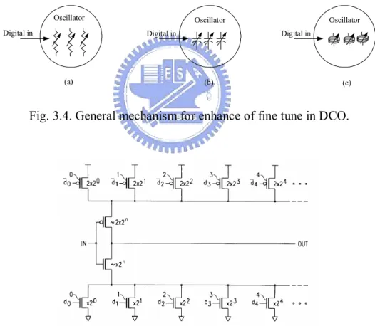
The basic skill to enhance the fine resolution of DCO is to enhance overall driving capability. The methods are to adjust the overall resistance (R), or to adjust capacitance (C), or to adjust inductance (L) as shown in Fig. 3.4.
Digital in Oscillator Digital in Oscillator Digital in Oscillator (a) (b) (c)
Fig. 3.4. General mechanism for enhance of fine tune in DCO.
Fig. 3.5. DCO with fine resolution constructed with current starved ring oscillator.
A well-known DCO is indicated in [37], the desired output frequency is directly synthesized through the operation of an eight-stage current-starved ring oscillator, on such stage is
illustrated in Fig. 3.5. Each inverting stage includes a pull-up leg of parallel binary-weighted transistors, and pull-down leg of parallel binary-weighted transistors each of the transistor on the pull-up leg or pull-down leg is controlled by a corresponding bit di of the control word D.
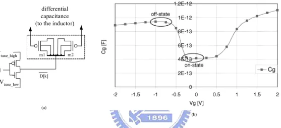
While acceptance frequency resolution is provided, the amount of integrated circuit chip area is extremely large. In addition, the layout of the DCO has to be full custom, which is very time consuming. D[k] m1 m2 Vtune_high differential capacitance (to the inductor)
Vtune_low D[k]
(a)
(b)
Fig. 3.6. DCO with differential capacitance for fine resolution (a). circuit structure. (b). Gate capacitance v.s. gate voltage for PMOS varactor (L=0.5 mm, W=0.6 mm) when source and
drain tied to GND.
Another DCO has significant resolution using a switched-capacitor bank for RF application is indicated in [54]. The LC tank DCO achieves very fine frequency resolution (23KHz) by using advanced 0.13-mm CMOS process. The switchable capacitance of the finest PMOS varactor is 38 attofarads as shown in Fig 3.6 where the D[k] is the digital control word. The differential capacitance is formed by transistor M1 and M2. However, this DCO suffers from one fundamental drawback. Due to the extremely small size of varactor, it requires intensive circuit layout and needs advanced lithography technology. It also needs to overcome Process variations, Voltage variations, and Temperature variations (PVT variations) before an acceptable performance can be achieved. And because of these complicated factors, they
often result in a long design cycle as the design product transfers to different process or design specifications are changed.
3.1.3 Fine Tune in Standard Cell Library
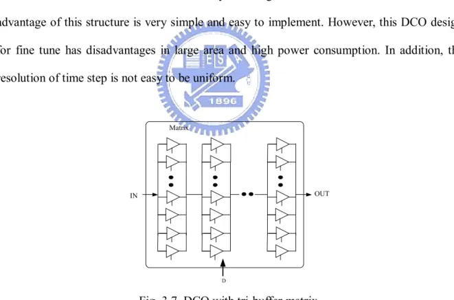
For most digital applications, a standard cell description of the digitally controlled oscillation simplifies the design, and it can be easily ported to different processes in a very short time period. One simple DCO design directly using an inverter as delay cell is reported in [46], but its resolution is not fine enough for most applications. The other example, a DCO consists of a bank of tri-state inverter buffers was proposed in [47-49] as shown in Fig. 3.7. The resolution of DCO can be controlled by enabling the numbers of tri-state buffers. The advantage of this structure is very simple and easy to implement. However, this DCO design for fine tune has disadvantages in large area and high power consumption. In addition, the resolution of time step is not easy to be uniform.
IN
D
OUT Matrix
Fig. 3.7. DCO with tri-buffer matrix.
Another example of DCO implemented by an and-or-inverter (AOI) cell and or-and-inverter (OAI) cell with two parallel tri-state inverters was proposed in [50]. The basic method is to adjust the driving capability with resistance control. This fine tune method of DCO cell has less area and power consumption than [47-49]. However, its resolution step is
non-uniform and sensitive to power-supply variation because it is based on AOI-OAI cell to change the delay resolution. In addition, this technique also requires an additional decoder for mapping AOI-OAI cell control inputs.
IN OUT AOI A1 B1 OAI A2 B2 1 1 EN1 EN2
Fig. 3.8. DCO with AOI-OAI as fine tuning cell.
The concept of timing vernier has been utilized in measurement [58]. A fine tune method in [59] uses the delay difference of NAND between different paths. For example, the capacitances and output strengths of different pins are approximately close for a NAND gate in standard-cell library. The timing delay difference from different input pins to the same output pin approximates to the intrinsic delay difference. The advantage is that the delay difference can be check directly from the standard-cell data sheet. However, the real routing, placement, and loading of the NAND gate in the chip will also influence the intrinsic delay difference. In addition, the on/off each switch will also cause fluctuation of timing difference.
IN Path1 Path2 Fsel-1 DT1=R Path3 Path4 Fsel-2 DT2=2R Path5 Path6 Fsel-3 DT3=4R Path7 Path8 Fsel-4 DT4=8R OUT
3.2 Digital Control Oscillator with DCVs
A delay control method has been successfully applied in delay locked loop as indicated in [71] based on path difference. The other similar concept was based on single path delay as indicated in [56].
(a) (b) Fig. 3.10. (a). Delay control in [71]. (b). Delay control in [56].
The proposed DCO, like most voltage-controlled oscillators or delay control, employs a frequency control mechanism located inside an oscillator block. Two parameters are used to modulate the output frequency of a ring oscillator, namely the propagation delay time of each delay cell, and the total number of delay cells in the closed loop. Generally, delay time resolution is more difficult to achieve than total delay time, because the transistor width/length (W/L) is fixed in a cell-based design. To deal with this problem, we developed a novel DCV using NOR/NAND gate in the fine-tuning cell design of DCO. The proposed DCO improves delay resolution and demonstrates monotonic delay behavior with respect to digital control codes. The proposed technique has been successfully verified on a test chip fabricated in a 0.35-mm 2P4M CMOS process.
Basically, two main techniques exist for designing a fine resolution in DCO with shunt capacitor. One technique changes the MOS driving strength dynamically using a fixed capacitance loading and achieves a fine resolution [55]. Meanwhile, the other uses the shunt
X1 X2 X4 X8 I O Control In Out xN In Out D0 D0 D0 x
capacitor technique to fine-tune the capacitance loadings and achieves high resolution [54,56]. Figure 3.11 shows the conventional control mechanism with the shunt capacitor circuit. In Fig.3.11, MC serves as a capacitor. The gate of transistor Mctrl (that is, Dctrl) controls the
discharge/charge current. Consequently, Dctrl can control the delay resolution from In to Out.
Fig. 3.11. Conventional digitally controlled mechanism with shunt capacitor.
3.2.1 Digitally Controlled Varactors
Figure 3.12(a) illustrates a novel varactor cell using a two-input NOR gate. As described in [60], the gate-to-channel capacitance contributes to total gate-capacitance. The proposed method controls the capacitance between gate and source or between gate and drain. In Fig. 3.12(a), the NOR gate-capacitance at node CL depends on control node D’s value. The total
gate-capacitance of transistors M2 and M3 varies with D input states. Figure 3.12 (b) shows the equivalent circuit of Fig. 3.12(a), an initial capacitance (CI) parallels with a capacitance
difference (ΔC). The D input controls the capacitance (ΔC) in the output (Out) node.
Fig. 3.12. Proposed DCV with two-input NOR gate. (a) Circuit with digital control. (b) Equivalent circuit with ΔC capacitance.
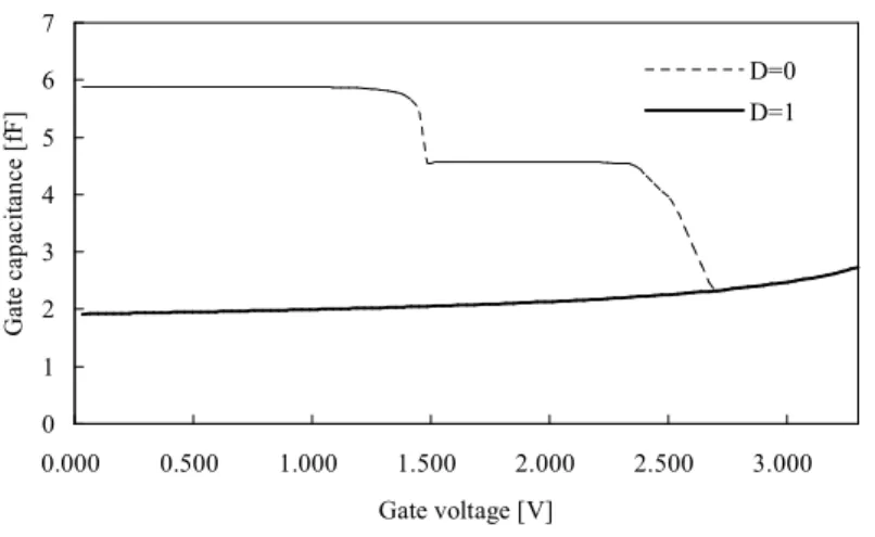
Figure 3.13 shows the gate-capacitance difference characteristic which is simulated using the HSPICE circuit simulator. The swing-averaged capacitance Caverage(D), as D-node is in the 0
state or in the 1 state, is given by
Caverage(D)= gate gate
Vdd dd dV D V C V ( , ) 1 0
ò
(3.4)where C(Vgate, D) denotes the simulated gate capacitance shown in Fig. 3.12. Based on Eq.
(3.4), ΔC denotes the capacitance difference between Caverage(0) and Caverage(1). Consequently,
the variable delay (ΔT) of the proposed DCV in different D states can be calculated easily using the following linear equation,
ΔT = Kload x ΔC (3.5)
where Kload denotes the delay factor of driving inverter. The Kload value of the driving inverter
is 0.535 (ns/pF) in target 0.35-mm 2P4M CMOS cell library. The ΔC of Fig. 3.13 is estimated to be around 2.8 fF. Therefore, ΔT of 1.49 ps (=0.535 * 2.8) is easily obtained. If N NOR gates are attached to the CL node, the max delay time variation becomes N*ΔT. Moreover,
different ΔT can be achieved as needed by changing the cell type of the driving inverter (i.e., change the Kload ).
0 1 2 3 4 5 6 7 0.000 0.500 1.000 1.500 2.000 2.500 3.000 Gate voltage [V] G at e ca pa ci ta nc e [f F ] D=0 D=1
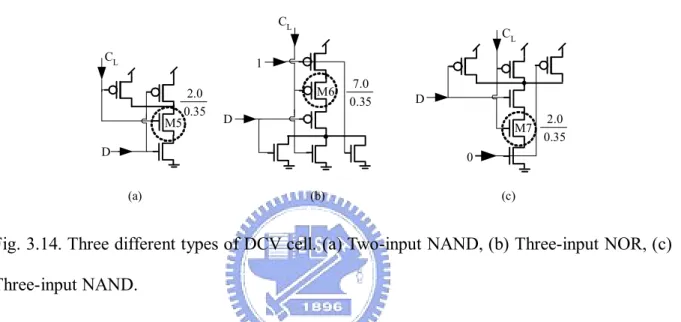
A NAND gate can also be applied to DCV design. Figure 3.14 illustrates three different DCVs: (a) two-input NAND gate, (b) three-input NOR gate, and (c) three-input NAND gate. For the three-input NOR and three-input NAND gate, an extra input pin is fixed to 1 and 0, respectively. The marked transistors (M5, M6, M7) produce a large capacitance difference under different D states.
M5 D CL (a) M6 1 D CL (b) 2.0 0.35 7.0 0.35 M7 D CL 0 (c) 2.0 0.35
Fig. 3.14. Three different types of DCV cell. (a) Two-input NAND, (b) Three-input NOR, (c) Three-input NAND.
Table 3.1 lists the comparisons among these DCVs. The three-input NAND/NOR gate varactor consumes less power than the 2-input NAND/NOR gate varactor, but it costs more area. Generally, the finer delay resolution can be obtained by decreasing MOS width of (M5, M6, M7).
3.2.2 Performance of the Digitally Controlled Varactors
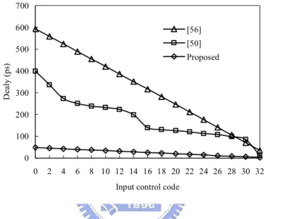
HSPICE circuit simulation is performed for estimating the performance of different type fine-tuning delay cell including the proposed DCV, pass transistor [56], and OAI cell [50] on a standard 0.35-mm CMOS 2P4M process. In this simulation, a series of 97 inverters are used in the coarse-tuning stage of the ring oscillator, and the proposed DCV serves as the fine-tuning delay cell. Totally, 32 DCVs are used in the fine-tuning delay cell (N=32).
0 100 200 300 400 500 600 700 0 2 4 6 8 10 12 14 16 18 20 22 24 26 28 30 32 Input control code
D ea ly ( ps ) [56] [50] Proposed
Fig. 3.15. Comparisons among the proposed DCV and other approaches.
Figure 3.15 shows the delay resolution of the fine-tuning stage and the proposed delay cell has finer resolution (about 1.43ps) than other circuits [50,56]. The delay cell proposed by [56] has very good linearity but poor resolution and it also has large transistor counts. Oppositely, OAI cell [50] has less transistor counts and less power consumption, but it has non-uniform linearity.
Figure 3.16 shows the proposed DCV under different PVT conditions: (Best: FF, 3.6V, 0 0C), (Typical: TT, 3.3V, 25 0C), and (Worst: SS, 3.0V, 125 0C). The delay resolution of the
proposed DCV ranges from 1.28 ps in the best case to 1.61 ps in the worst case. It demonstrates the effectiveness of the proposed DCV to overcome PVT variations.
0 10 20 30 40 50 60 0 2 4 6 8 10 12 14 16 18 20 22 24 26 28 30 32 Input control code
D C V D el ay ( ps ) Best Typical Worst
Fig. 3.16. The proposed DCV using two-input NOR under different PVT conditions.
3.3
Structure of the Proposed DCO
3.3.1 Structure of DCO and Design Guide
Fig. 3.17 illustrates the structure of the proposed cell-based DCO with 15 bits binary weighted control (000016 ~ 7FFF16). The proposed DCO structure is separated into two stages:
the coarse-tuning stage and the fine-tuning stage. The higher seven bits of the control code are for coarse-tuning stage, and lower eight bits are for the fine-tuning stage. The coarse-tuning stage uses a 128-to-1 path selector for delay-chain selection. This selector is implemented by multistage tri-state buffers to reduce the loading effects of coarse-tuning buffers. The coarse decoder of the DCO decodes the 7 (=log2(128)) bits control code into 128 control signals.
This architecture has the advantage that operating frequency of DCO can be easily modified according to different specifications. The TPHL + TPLH ( = Tbuffer) of one coarse delay cell is
about 385 ps in target 0.35-mm 2P4M CMOS standard cell library.
To increase the frequency resolution of the DCO, the fine-tuning stage is divided into fine1 and fine2 stages which are added after the coarse-tuning stage. The fine1 stage consists of 32
![Fig. 2.6 shows the proposed ADPLL with fixed high-speed clock and output accumulator in [3]](https://thumb-ap.123doks.com/thumbv2/9libinfo/8343998.176151/34.892.132.811.864.1086/shows-proposed-adpll-fixed-speed-clock-output-accumulator.webp)
![Figure 2.8. ADPLL with direct DCO synthesis clock [37].](https://thumb-ap.123doks.com/thumbv2/9libinfo/8343998.176151/36.892.156.796.822.1029/figure-adpll-direct-dco-synthesis-clock.webp)

![Fig. 2.11. PLL frequency synthesizer with DPFD [62]. (a) Functional block diagram. (b) Structure of DPFD](https://thumb-ap.123doks.com/thumbv2/9libinfo/8343998.176151/41.892.253.702.163.320/frequency-synthesizer-dpfd-functional-block-diagram-structure-dpfd.webp)