國
立
交
通
大
學
電子工程學系 電子研究所碩士班
碩 士 論 文
在鍺通道金氧半場效電晶體上使用後沉積氧化製造
二氧化鉿/三氧化二鋁/氧化鍺/鍺之閘極介電層堆疊
結構的研究
Investigation of HfO
2/Al
2O
3/GeO
x/Ge Gate Stacks
Fabricated by Post Deposition Oxidation on
Ge-Channel MOSFETs
研 究 生:吳哲鎮
指導教授:簡昭欣 教授
在鍺通道金氧半場效電晶體上使用後沉積氧化製造
二氧化鉿/三氧化二鋁/氧化鍺/鍺之閘極介電層堆疊
結構的研究
Investigation of HfO2/Al2O3/GeOx/Ge Gate Stacks
Fabricated by Post Deposition Oxidation on
Ge-Channel MOSFETs
研 究 生:吳哲鎮 Student:Che-Chen Wu
指導教授:簡昭欣 教授 Advisor:Dr. Chao-Hsin Chien
國 立 交 通 大 學
電 子 工 程 學 系 電 子 研 究 所 碩 士 班
碩 士 論 文
A Thesis
Submitted to Department of Electronics Engineering and Institute of Electronics College of Electrical and Computer Engineering
National Chiao Tung University In Partial Fulfillment of the Requirements
For the Degree of Master In Electronics Engineering
October 2012
Hsinchu, Taiwan, Republic of China
在鍺通道金氧半場效電晶體上使用後沉積氧化
製造二氧化鉿/三氧化二鋁/氧化鍺/鍺之閘極介
電層堆疊結構的研究
學生:吳哲鎮
指導教授:簡昭欣 教授
國立交通大學
電子工程學系 電子研究所碩士班
摘要
在這篇論文之中,首先我們研究了在原子層沉積三氧化二鋁介電層之後使用 後沉積氧化方式,藉由快速升溫退火爐通氧氣退火在鍺介面上形成薄的 GeOx介 電層之鍺 P 型金氧半電容。我們藉由後沉積氧化方式將等效氧化層厚度降至 1.41 奈米,並且使用及探討了電導法(conductance method)來萃取介面缺陷電荷密度。 使用後沉積氧化方式之試片與一般直接熱成長二氧化鍺之試片比較起來有較小的介面缺陷電荷密度,而我們也研究了 GeOx /Ge 之介面缺陷電荷密度與 GeOx
厚度的關係。我們認為之所以用較高溫度的後沉積氧化方式會有較厚的 GeOx介
電層以及較小的介面缺陷電荷密度是因為在較高溫度下會有較大的鍺三價波峰 存在。介面缺陷電荷密度再經由 300 度 30 分鐘氫氣氮氣混合之熱退火可被降低, 介面缺陷電荷密度的質在熱退火後下降了 16% ~ 44%。而在熱退火後我們也發現 了平帶電壓往正的方向移動以及較小的電壓遲滯現象。我們最後決定選用二氧化
鉿/三氧化二鋁之閘極介電層以及使用後沉積氧化方式 520 度 3 分鐘這組條件來 繼續進行元件的製造。 其次,我們研究了氫氣氮氣混合之熱退火對鍺的接面以及元件特性之影響, 包含了 P 型金氧半場效電晶體以及 N 型金氧半場效電晶體。在熱退火之後,我 們的 p+ n 接面以及 P 型金氧半場效電晶體的電流開關比分別是 4 orders 與 1.4×10³, 以及較佳的次臨界擺幅(165mV/dec);而在 n+ p 接面以及 N 型金氧半場效電晶體 方面,電流開關比分別是 3.5 orders 與 2.3×10³,次臨界擺幅則是 151mV/dec。對 P 型以及 N 型兩者金氧半場效電晶體而言,在氫氣氮氣混合之熱退火後,源極汲 極串聯阻抗上升,電洞載子遷移率提高,電洞載子遷移率波峰達到 375 cm2 /Vs。 綜合比較 300 度 30 分鐘氫氣氮氣混合之熱退火對 P 型以及 N 型兩者金氧半場效 電晶體的優缺點,在熱退火之後,平帶電壓會往正的方向移動,有較高的驅動電 流,較佳的次臨界擺幅以及較高的電洞載子遷移率,然而源極汲極串聯阻抗卻會 上升。 最後,我們研究了氫氣氮氣混合之熱退火對磊晶鍺在絕緣層上覆矽金氧半場 效電晶體的影響,包含了磊晶 60 奈米鍺以及 30 奈米鍺在絕緣層上覆矽。對 P 型以及 N 型兩者金氧半場效電晶體而言,在熱退火之後,平帶電壓會往正的方 向移動,較佳的次臨界擺幅,較高的驅動電流,較低的漏電流,較大的源極汲極 串聯阻抗以及較高的電洞載子遷移率,電洞載子遷移率波峰達到 313 cm2 /Vs(磊 晶 60 奈米鍺)以及 194 cm2 /Vs(磊晶 30 奈米鍺)。磊晶 30 奈米鍺在絕緣層上覆矽 金氧半場效電晶體有較佳的次臨界擺幅,而磊晶 60 奈米鍺在絕緣層上覆矽金氧 半場效電晶體則是有較大的驅動電流以及電洞載子遷移率。
Investigation of HfO
2/Al
2O
3/GeO
x/Ge Gate
Stacks Fabricated by Post Deposition Oxidation
on Ge-Channel MOSFETs
Student:Che-Chen Wu Advisor:Dr. Chao-Hsin Chien
Department of Electronic Engineering & Institute of Electronics
National Chiao Tung University
ABSTRACT
In this thesis, firstly, germanium MOS capacitors using post deposition oxidation method to form a thin GeOx interfacial layer by oxidizing Ge surface beneath an ALD
Al2O3 layer using high-k RTO was fabricated and analyzed electrically. The EOT
value was scaled down to 1.41 nm by PDO. Theory of the conductance method was discussed in detail, and utilizing it to extract the interface state density. The post oxidation deposition samples have less interface state densitythan thermal GeO2
samples, and the Dit of GeOx/Ge MOS interface controlled by the GeOx thickness has
been studied. We think the less interface state density is because of the thicker GeOx
interfacial layer and larger Ge3+ peak which the higher post deposition oxidation
temperature grown. Interface state density was shown to be reduced through 300°C 30 minutes forming gas annealing, the Dit value has been reduced 16% ~ 44%. The
positive VFB shift and lower C-V hysteresis is shown in the samples after FGA. The
HfO2/Al2O3 gate stack with PDO 520°C 3min was selected to be the best condition to
Secondly, we investigated the effect of FGA on Ge junction and device characteristics, including both PMOSFET and NMOSFET. On/off ratio of our p+n
junction and PMOSFET reached 4 orders and 1.4×10³ respectively, with better
subthreshold swing (165mV/dec) obtained after FGA. And on/off ratio of our n+p
junction and NMOSFET reached 3.5 orders and 2.3×10³ respectively, with better
subthreshold swing (151mV/dec) obtained after FGA. For both PMOSFETs and NMOSFETs, the larger series resistance and higher hole mobility are observed after FGA, a peak hole mobility of 375 cm2/Vs after FGA is obtained. Pros and cons of
FGA at 300°C 30 min on both PMOSFET and NMOSFET were summarized according to our experimental data. Positive VFB shift, higher drive current, better
subthreshold swing and higher hole mobility are obtained after FGA, while series resistanceis increased after FGA.
Finally, we investigated the effect of FGA on epi-Ge on SOI MOSFETs characteristics, including epi-60nm Ge on SOI and epi-30nm Ge on SOI. For both PMOSFETs and NMOSFETs, the positive Vth shift, better subthreshold swing, higher
on current, lower off current and higher RSD are obtained after FGA. Also, the higher
hole mobility is observed, a peak hole mobility of 313 cm2/Vs for epi-60nm
PMOSFET and 194 cm2/Vs for epi-30nm NMOSFET after FGA are obtained.
Epi-30nm Ge on SOI MOSFETs have better subthreshold swing, while epi-60nm Ge on SOI MOSFETs have larger on current and higher hole mobility.
誌謝
兩年多的研究所生涯,說長不長,說短不短,終於要告一段落了。這一篇論 文能夠順利完成,首先要感謝我的指導老師-簡昭欣教授。老師不只在學業上給 予我很大的幫助,在待人處事上也是教了我不少東西,老師總是不斷叮嚀我們在 未來職場上應有的態度,生怕我們一時疏忽給了主管不好的印象。相信在老師的 諄諄教誨下,我在未來職場上的路應該可以走得平順一些,也期許自己在公司裡 能夠有好的表現,不辜負老師的期待。 政庭學長,感謝你在這兩年來的幫忙與指導,一直幫我解決實驗上遇到的問 題,沒有你的幫忙,這些電容、元件是不可能做出來的,在這裡衷心的感謝你, 也希望你接下來的實驗一切順利。哲偉學長,總是拿一些奇怪的東西問你,你也 都不厭其煩的一一回答我,真的很謝謝你,畢業之後聽不到你打嘴砲了該怎麼辦 啊。信淵學長,每次量測時都要麻煩你來解決各式各樣的怪問題,沒有你我的量 測會變得很辛苦的,期待之後還有機會跟你一起打球。韋志學長,你一步一步的 帶我做實驗,讓我從什麼都不會到現在可以獨立做出元件。宏碁學長,奈米中心 的扛壩子,頂著你的光環讓我在實驗上沒遇到太多困難。家豪學長、宇彥學長、 宗佑學長、昶智學長,感謝你們在大大小小事情上的幫忙。 小林、酷奇、就舉,並肩作戰的好友們,讓我在做實驗的時候不孤單,希望 之後還能常常有機會一起吃飯。小龜、主元、邦聖、純敏,目前在正水深火熱的 學弟妹們,希望你們到時候能準時畢業。 當然,最重要的是要感謝我的父母,沒有他們在背後默默的支持我,讓我無 後顧之憂的專心在學業上衝刺,我想我不會有今天的成就,我一定會好好孝順你 們的。 最後,凡是有幫助過我大大小小的人,我都由衷的感謝你們,也祝福所有的 人都能心想事成。Contents
Abstract (Chinese) ... I Abstract (English) ... III Acknowledgement ... V Contents ... VI Table Captions ... VIII Figure Captions ... IX
Chapter 1 ... 1
1.1 General Background ... 1
1.2 Motivation ... 2
1.3 Scope and Organization of the Thesis ... 3
References (Chapter 1) ... 5
Chapter 2 ... 7
2.1 Introduction ... 7
2.2 Fabrication of ALD- HfO2/Al2O3/GeOx/Ge MOSCAP ... 9
2.3 Characteristics of Ge MOSCAP ... 10
2.3.1 C-V Characteristics of Ge MOSCAP ... 10
2.3.2 Conductance Method ... 11
2.4 Effect of FGA on Electrical Characteristics ... 15
2.5 Conclusions ... 16
References (Chapter 2) ... 18
Chapter 3 ... 37
3.2 Fabrication of Gate-Last Ge MOSFET ... 38
3.3 Effect of FGA on Ge MOSFET Electrical Characteristics ... 39
3.3.1 Ge junction Characteristic ... 39 3.3.2 Device Characteristic ... 40 3.4 Conclusions ... 43 References (Chapter 3) ... 45 Chapter 4 ... 56 4.1 Introduction ... 56
4.2 Fabrication of Gate-Last Epi-Ge on SOI MOSFET ... 57
4.3 Effect of FGA on Epi-Ge on SOI MOSFET Electrical Characteristics ... 59
4.4 Conclusions ... 60
References (Chapter 4) ... 62
Table Captions
Table 1.1 Material properties of bulk Ge, Si, GaAs, and InAs at 300K are compared . 6
Table 2.1 The overview of a-d samples with different PDA condition. ... 22
Table 2.2 The overview of A-D samples with different RTO condition. ... 22
Table 2.3 The C-V hysteresis with different PDA condition. ... 25
Table 2.4 The C-V hysteresis with different post deposition oxidation condition. ... 25
Table 2.5 The C-V hysteresis with different post deposition oxidation condition before FGA. ... 34
Table 2.6 The C-V hysteresis with different post deposition oxidation condition after FGA... 34
Figure Captions
Fig. 2.1 The process flow and device structure with different PDA condition. ... 20
Fig. 2.2 The process flow and device structure with different post deposition
oxidation condition. ... 21
Fig. 2.3 The multi frequency C-V of Ge MOSCAPs with different PDA condition. (a)
RTO thermal GeO2 520°C 30sec with PDA 500°C 60sec N2 (b) RTO thermal
GeO2 520°C 30sec with PDA 500°C 60sec O2 (c) post deposition oxidation
520°C 3min with PDA 500°C 60sec N2 (d) post deposition oxidation 520°C
3min with PDA 500°C 60sec O2. ... 23
Fig. 2.4 The multi frequency C-V of Ge MOSCAPs with different post deposition oxidation condition. (a) Al2O3/Al2O3 with post deposition oxidation GeO2 520°C
3min (b) Al2O3/Al2O3 with post deposition oxidation GeO2 550°C 3min (c)
HfO2/Al2O3 with post deposition oxidation GeO2 520°C 3min (d) HfO2/Al2O3
with post deposition oxidation GeO2 550°C 3min. ... 24
Fig. 2.5 The XPS spectra of Al2O3/GeOx/p-Ge with different PDO and thermal grown
GeOx condition. ... 26
Fig. 2.6 Equivalent circuits for conductance measurements; (a) MOSCAP with
interface trap time constant τit = RitCit , (b) simplified circuit of (a), (c) measured
circuit, (d) including series rs resistance and tunnel conductance Gt . ... 27 Fig. 2.7 The behavior of the interface trap time constant at room temperature as a
function of capture cross section determines the part of interface traps in the bandgap observable in the MOS admittance characteristic. ... 28
Fig. 2.8 2.5GP/ωq versus frequency of Ge MOSCAPs with different PDA condition.
(a) RTO thermal GeO2 520°C 30sec with PDA 500°C 60sec N2 (b) RTO thermal
GeO2 520°C 30sec with PDA 500°C 60sec O2 (c) post deposition oxidation
520°C 3min with PDA 500°C 60sec N2 (d) post deposition oxidation 520°C
3min with PDA 500°C 60sec O2. ... 29
Fig. 2.9 2.5GP/ωq versus frequency of Ge MOSCAPs with different post deposition
oxidation condition. (A) Al2O3/Al2O3 with post deposition oxidation GeO2 520°C
3min (B) Al2O3/Al2O3 with post deposition oxidation GeO2 550°C 3min (C)
HfO2/Al2O3 with post deposition oxidation GeO2 520°C 3min (D) HfO2/Al2O3
with post deposition oxidation GeO2 550°C 3min. ... 30
Fig. 2.10 Dit profiles of each samples near midgap (a) samples a b c d and (b) samples
A B C D. ... 31
Fig. 2.11 A band diagram showing the weak inversion response (a) and the general
equivalent circuits used to model the MOS capacitor C-V and G-V
characteristics across the bandgap for an n-type capacitor. The first circuit (b) models one trap only: Cox is the oxide capacitance, Cinv the inversion capacitance,
Cdep the depletion (and accumulation) capacitance, CT the trap capacitance and
Gn and Gp electron and hole trap conductances. For a distribution a series of
Y-circuits is used (c)... 32
Fig. 2.12 The multi frequency C-V of Ge MOSCAPs with different post deposition
oxidation condition after FGA. (a) Al2O3/Al2O3 with post deposition oxidation
GeO2 520°C 3min (b) Al2O3/Al2O3 with post deposition oxidation GeO2 550°C
3min (c) HfO2/Al2O3 with post deposition oxidation GeO2 520°C 3min (d)
HfO2/Al2O3 with post deposition oxidation GeO2 550°C 3min. ... 33
Fig. 2.13 2.5GP/ωq versus frequency of Ge MOSCAPs with different post deposition
GeO2 520°C 3min (b) Al2O3/Al2O3 with post deposition oxidation GeO2 550°C
3min (c) HfO2/Al2O3 with post deposition oxidation GeO2 520°C 3min (d)
HfO2/Al2O3 with post deposition oxidation GeO2 550°C 3min. ... 35
Fig. 2.14 Dit profiles of each samples near midgap (a) samples A B C D without FGA
(b) samples A B C D with FGA. ... 36
Fig. 3.1 The process flow and device structure of Ge MOSFET... 46
Fig. 3.2 I–V characteristics of p+n and n+p junctions, before and after performing
FGA. (a) p+n junction (b) n+p junction ... 47
Fig. 3.3 Effects of FGA at 300 oC on the PMOSFET. (a) ID-VG characteristic. (b)
IS-VG characteristic. ... 48
Fig. 3.4 Effects of FGA at 300 oC on the NMOSFET. (a) ID-VG characteristic. (b)
IS-VG characteristic. ... 49
Fig. 3.5 Effects of FGA at 300 oC on the ID-VG characteristics (a) PMOSFET. (b)
NMOSFET. ... 50
Fig. 3.6 (a)The schottky junction tunneling. (b)Series resistance from Terada and
Muta method. ... 51
Fig. 3.7 Schematic for gate-to-channel capacitance measurements for (a) VGS < VT,(b)
VGS > VT... 52
Fig. 3.8 Effects of FGA at 300 oC on (a) Qinv versus VG plot and (b) gd versus VG plot.
... 53
Fig. 3.9 Effective mobility versus inversion charge is plotted with and without FGA at
300 oC. ... 54
Fig. 3.10 (a) Schematics of the effect of the low conductance-band offset on the
electron trapping by the slow traps and the bulk traps in the NMOS inversion regime. (b) Dit energy distribution of acceptor and donor DB surface states and
Fig. 4.1 XRD data of epitaxial Ge on SOI. Higher Ge (004) peak indicates 60nm Ge has higher quality on SOI. ... 63
Fig. 4.2 (a) (b) TEM image of epi-60nm Ge on SOI. Lower dislocation density with
smooth surface is observed. ... 64
Fig. 4.3 (a) (b) TEM image of epi-30nm Ge on SOI. High dislocation density exists in
Ge film accompanying with high roughness. ... 65
Fig. 4.4 The two epi-Ge on SOI substrate structures. (a) epi-60nm Ge on SOI. (b)
epi-30nm Ge on SOI. ... 66
Fig. 4.5 The process flow and device structure of epi-Ge on SOI MOSFET ... 68
Fig. 4.6 Effects of FGA at 300 oC on the PMOSFET. (a) Epi-60nm Ge on SOI ID-VG
characteristic. (b) Epi-60nm Ge on SOI IS-VG characteristic. (c) Epi-30nm Ge on
SOI ID-VG characteristic. (d) Epi-30nm Ge on SOI IS-VG characteristic. ... 69
Fig. 4.7 Effects of FGA at 300 oC on the ID-VG characteristics of PMOSFETs (a)
Epi-60nm Ge on SOI. (b) Epi-30nm Ge on SOI. ... 70
Fig. 4.8 Effective mobility versus inversion charge is plotted with and without FGA at
300 oC on PMOSFET. (a) Epi-60nm Ge on SOI. (b) Epi-30nm Ge on SOI. ... 71
Fig. 4.9 Effects of FGA at 300 oC on the NMOSFET. (a) Epi-60nm Ge on SOI ID-VG
characteristic. (b) Epi-60nm Ge on SOI IS-VG characteristic. (c) Epi-30nm Ge on
SOI ID-VG characteristic. (d) Epi-30nm Ge on SOI IS-VG characteristic. ... 72
Fig. 4.10 Effects of FGA at 300 oC on the ID-VG characteristics of NMOSFET (a)
Chapter 1
Introduction
1.1 General Background
In 1947, the first transistors were fabricated in Bell Laboratories using bulk germanium as the semiconducting material by John Bardeen, Walter Brattain and William Shockley. Then, the integrated circuit which made of Germanium was invented by Jack Kilby in 1958. Germanium was the predominant material for
solid-state devices through the 1950s and early 1960s. However, during the 1960s, the first metal oxide semiconductor field effect transistors (MOSFETs) fabricated by Dawon Kahng and Martin Atalla was made of silicon, and then germanium was largely replaced with silicon. There are many reasons why germanium was largely replaced with silicon, such as the larger bandgap of silicon resulting in lower leakage currents and the excellent quality and stability of thermal SiO2 as a gate dielectric for
silicon compared with the water soluble and thermal instable GeO2 [1]. Therefore,
Si-based MOSFETs have become the driving force for the semiconductor industry in the last four to five decades.
Recently, it has been increasingly difficult to further improve the performances of Si complementary metal–oxide–semiconductor (CMOS) devices through the conventional device scaling [2]. The physical dimensions have been continually reduced to double the number of transistors on a chip every eighteen months
according to Moore’s Law [3]. The decrease in transistor dimensions has led to increase in microprocessor performance. With the reduction in device dimensions of MOSFETs, silicon dioxide films, which used as a gate dielectric, have been scaled down to keep the same control over the channel. Devices with thinner dielectric could improve the short channel effect. But beyond the 16nm node, CMOS technology using Si channel has encountered formidable challenges, as further scaling in the transistors may not provide device performance advantages [4]. In order to maintain Moore’s Law, mobility enhancement has become a key technology. Ge has been considered as one promising candidate for replacing Si, because of not only its much higher intrinsic carrier mobility but also the compatibility with the conventional Si integration technologies.
1.2 Motivation
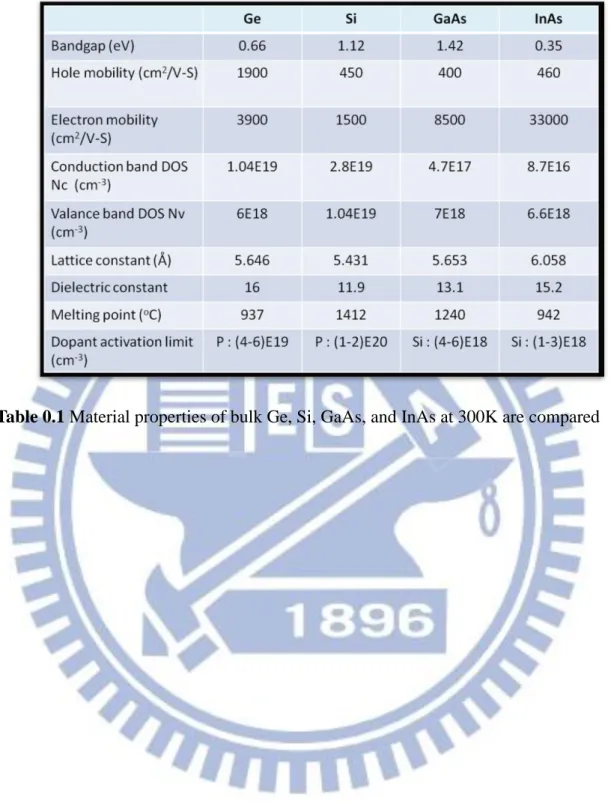
As shown in Table 1.1, the material properties of bulk Si, Ge, GaAs, and InAs at 300K are compared [5]. Germanium has better electron (3900 versus 1500 cm2/Vs)
and hole (1900 versus 450 cm2/Vs) bulk mobility for Ge over Si. The lower bandgap
(0.66eV versus 1.12eV) characteristic of Ge enables to lower the Schottky barrier height and contact resistance than Si. However, Ge has several practical problems. First, the lower bandgap of germanium resulting in higher leakage currents. Second, Ge oxides are water soluble and thermal instable, they are easy to rinsed of during the fabrication process. Third, it is difficult to achieve a high-quality oxide/Ge interface due to the bad surface properties of Ge.
Recently, the Ge PMOSFETs with high hole mobility values have been
MOS interfaces [6]. However, the thick GeO2 gate stacks may leads larger equivalent
oxide thicknesses (EOTs). In order to scale down EOT, development of
high-k/Germanium gate stack is necessary. High interface quality and small EOT is essential for Ge to be used as an alternative high mobility channel material for future technology nodes. Ge PMOSFETs have been realized with direct high-k/Ge gate stacks [7]. Because of the poor MOS interfaces, these Ge PMOSFETs show quite low mobility values. Therefore, it is necessary to develop high-k/Ge gate stacks with both thin EOT and low interface state density (Dit). Employing a thin GeO2 interfacial
layer (IL) is a promising solution [8].
1.3 Scope and Organization of the Thesis
The promising high-mobility substrate material, Ge, was investigated in this thesis. In this thesis, we focus on using post deposition oxidation method to form a thin GeOx ILby oxidizing Ge surface beneath a thin atomic layer deposition (ALD)
Al2O3 layer using high-k rapid thermal oxidation (RTO). The thesis is divided into
five chapters and arranged as follows:
Chapter 1, a brief overview of background and motivation is described.
Chapter 2, Ge PMOS capacitors using post deposition oxidation method to form
a thin GeOx IL by oxidizing Ge surface beneath a ALD Al2O3 layer using high-k RTO
was fabricated, the dependence of the GeOx/Ge interface qualities on the post
deposition oxidation conditions such as post deposition oxidation temperature and post deposition annealing ambient was investigated. Theory of the conductance
different sample. The effect of forming gas annealing (FGA) on PMOS capacitors was also investigated.
Chapter 3, both germanium NMOSFET and PMOSFET were fabricated using
post deposition oxidation method to form a thin GeOx IL by oxidizing Ge surface
beneath a ALD Al2O3 layer using high-k RTO. Effect of FGA on both NMOSFET
and PMOSFET junctions and device electrical characteristic was studied, including ID-VG, IS-VG, ID-VD, subthreshold swing and series resistance. The mobility extracted
from split C-V of both NMOSFET and PMOSFET were investigated, with and without FGA.
Chapter 4, both germanium NMOSFET and PMOSFET were fabricated on
epitaxial Ge on thin SOI substrates with two different structures, respectively. Effect of FGA on both NMOSFET and PMOSFET device electrical characteristic was studied, including ID-VG, IS-VG,ID-VD, subthreshold swing and series resistance. The
mobility extracted from split C-V of both NMOSFET and PMOSFET were investigated, with and without FGA.
Chapter 5, we summarized all experimental results in this thesis, gave the
References (Chapter 1)
[1] D. P. Brunco, B. De Jaeger, G. Eneman, J. Mitard, G. Hellings, and A. Satta et al., “Germanium MOSFET Device: Advances in Materials Understanding, Process Development, and Electrical Performance”, J. Electrochem. Soc. vol. 155, pp. H552-H561, 2008.
[2] H. Shang, M. M. Frank, E. P. Gusev, J. O. Chu, S. W. Bedell, K. W. Guarini, and M. Ieong, “Germanium channel MOSFETs: Opportunities and challenges,”
IBM J. Res. Develop., vol. 50, no. 4/5, pp. 377–386, Sep. 2006.
[3] G. E. Moore, “Cramming more components onto integrated circuits.” Electronics, vol. 38, pp. 114, 1965.
[4] L.K. Chu, R.L. Chu, T.D. Lin, W.C. Lee, C.A. Lin, M.L. Huang, Y.J. Lee, J. Kwo, M. Hong, “Effective passivation and high-performance
metal–oxide–semiconductor devices using ultra-high-vacuum deposited high-k dielectrics on Ge without interfacial layers,” Solid-State Electron, vol. 54, pp. 965, 2010.
[5] M. Levinshtein, S. Rumyantsev, and M. Shur, “Handbook Series on
Semicoductor Parameters Volume 1 : Si, Ge, C(diamond), GaAs, GaP, InAs, InP, InSb,” World Scientific, Singapore, 1996.
[6] Y. Nakakita, R. Nakane, T. Sasada, H. Matsubara, M. Takenaka, and S. Takagi, “Interface-controlled self-align source/drain Ge pMOSFETs using
thermally-oxidized GeO2 interfacial layers,” in IEDM Tech. Dig., pp. 877–880 , 2008.
[7] R. Xie, T. H. Phung, W. He, Z. Sun, M. Yu, Z. Cheng, and C. Zhu,“High mobility high-k/Ge pMOSFETs with 1 nm EOT—New concept on interface engineering and interface characterization,” in IEDM Tech. Dig., pp. 393–396, 2008.
[8] R. Zhang, T. Iwasaki, N. Taoka, M. Takenaka, S. Takagi, “High-Mobility Ge pMOSFET With 1-nm EOT Al2O3/GeOx/Ge Gate Stack Fabricated by Plasma
Chapter 2
Ge PMOSCAP HfO2/Al2O3
/GeO
x/Ge Gate Stack
Fabricated by Post deposition oxidation
2.1 Introduction
With the reduction in device dimension of silicon MOSFETs, gate dielectric had to scale down to keep the same control over the channel. In other words, the thickness of SiO2 must continue to scale down with channel length. However, when the
thickness of SiO2 decrease to less than 1.6 nm, gate leakage current becomes
significantly high due to direct tunneling. It appears that the continued scaling of silicon MOSFETs faced a physical obstacle. Replacing SiO2 with physically thicker
layer of new oxide with higher k had become essential to Si.
Recently, the successful of high-k dielectric on Si had helped the development of Ge MOSFET, because the gate dielectrics are no longer restricted to the thermal oxide. Development of high-k/Ge gate stack with high interface quality and small EOT is important for Ge to be used as a high mobility channel material. High-k gate
dielectrics like Al2O3 [1] and HfO2 [2] have been studied on Ge, showing promising
results in terms of low EOT. Al2O3 has wide bandgap energy, large conduction and
valance band offset, and high thermodynamic stability. Also, Al2O3 has higher
energy and band offset, and its dielectric constant value is even higher than Al2O3.
However, there is a problem in formation of the gate dielectric on germanium substrate. Germanium oxide is thermally unstable and water soluble, eliminating the formation of GeOx at the interface between high-k dielectric and Ge substrate is
important to form high quality gate stack on Ge. While direct high-k/Ge gate stacks have poor interface quality, interface passivation become a key challenge to improve the interface of high-k/Ge gate stacks. Recently, Ge MOSFETs using thick thermally grown GeO2/Ge gate stacks (EOT>20 nm) with low Dit have been reported to provide
high hole and electron mobility [3]. To have gate stacks satisfying both thin EOT and low Dit is necessary, employing a thin GeO2 interfacial layer is a promising solution
[4]. However, because of the damages introduced by the high-k deposition, depositing high-k films directly on an ultrathin GeO2/Ge MOS structure significantly degrades
the MOS interface and generates large amounts of Dit [5]. It is very difficult to have
thin EOT and low Dit simultaneously.
Using high-k RTO post deposition oxidation method to form a thin GeOx ILby
oxidizing Ge surface beneath a thin ALD Al2O3 layer is a promising solution. Al2O3
layer could be a protecting layer to prevent the damage introduced by the high-k deposition to the GeOx IL, and it also could be an oxygen barrier that suppresses the
growth of unnecessarily thick GeOx IL [6]. It has been found that Dit at the GeOx/Ge
interface increases with a decrease in the thickness of the GeOx IL.
In this chapter, the Ge PMOSCAPs are fabricated on Ge substrate with
HfO2/Al2O3/GeOx/Ge gate stacks by post deposition oxidation. The reason why we
didn’t use HfO2/GeOx/Ge gate stack is the intermixing between HfO2 and GeOx films,
which may increase Dit [7], almost no intermixing between Al2O3 and GeOx films.
Therefore, Al2O3 layer prevent not only the damage introduced by the high-k
the GeOx/Ge interface qualities on the post deposition oxidation conditions such as
post deposition oxidation temperature and post deposition annealing ambient was investigated. Theory of the conductance method was discussed in detail, and utilizing it to extract the interface state density for different sample. The effect of forming gas annealing (FGA) on PMOS capacitors was also investigated.
2.2 Fabrication of ALD- HfO
2/Al
2O
3/GeO
x/Ge MOSCAP
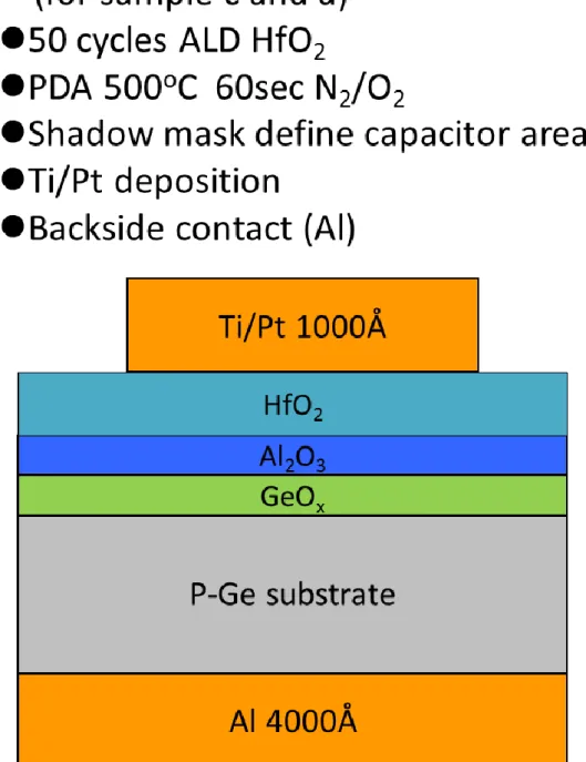
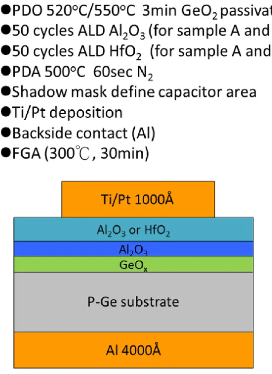
(100)-oriented p-Ge substrates with resistivity ca. 0.01Ω·cm ~ 0.05Ω·cm were used for MOSCAP fabrication. Before gate dielectric formation, all of the samples were pre-cleaned by diluted HF (20:1) and DI water rinsing to remove the native oxide, followed by 10 cycles ALD-Al2O3 thin film grown on each sample at 250°C, a
thin GeOx layer being formed by RTO post deposition oxidation to passivate the Ge
surface, with oxidation condition 520°C 3min and 550°C 3min. A 50 cycles HfO2
layer was deposited by ALD at 250°C. Post deposition annealing at 500°C 60sec with O2 and N2, respectively. Then,1000 Å Ti/Pt was deposited by sputter and the
capacitors front electrodes were patterned through shadow mask, while a thermal coater 4000 Å Al layer was deposited as the backside contact.
Forming gas annealing (FGA) at 300°C in a H2/N2 (5%) mixed ambient for 30
minutes was performed to investigate the effect of FGA on electrical characteristic. The process flow and device structure are shown in Fig. 2.1, Fig. 2.2. And the overview of all samples are shown in Table 2.1, Table 2.2.
2.3 Characteristics of Ge MOSCAP
2.3.1 C-V Characteristics of Ge MOSCAP
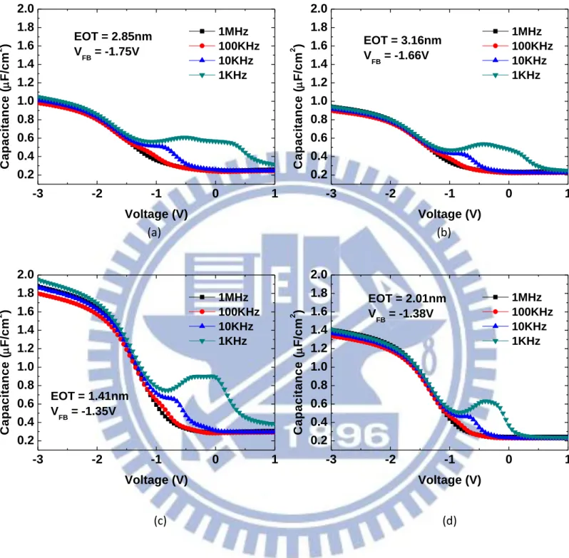
Fig. 2.3 shows the multi frequency C-V of Ge MOSCAPs with different PDA
condition. We can see that the MOSCAPs used post deposition oxidation GeOx have
smaller EOT than RTO thermal grown GeO2, which means Al2O3 layer could be an
oxygen barrier that suppresses the growth of unnecessarily thick GeOx ILs. A negative
flat band voltage (VFB) shift is often observed for Ge MOS capacitors, its origin has
not yet been addressed [8]. The positive VFB shift is shown in post deposition
oxidation GeOx samples compared with thermal grown GeO2. The larger EOT is
shown in PDA O2 condition compared with PDA N2, we think that the larger EOT of
PDA O2 is due to the growth of thicker GeOx ILs.
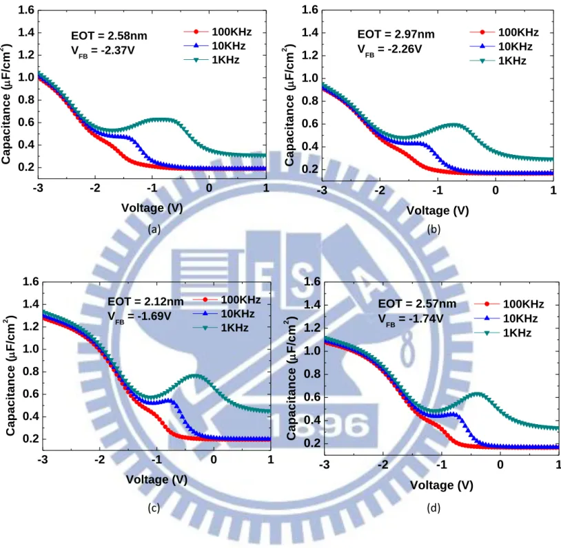
Fig. 2.4 shows the multi frequency C-V of Ge MOSCAPs with different post
deposition oxidation condition. The EOT value was scaled down to 1.41nm for
HfO2/Al2O3 with post deposition oxidation GeOx 520°C 3min sample. We can see that
the MOSCAPs with higher post deposition oxidation temperature have larger EOT and hump become much smaller in depletion region, we supposed that the higher post deposition oxidation temperature may increase GeOx interfacial layer thickness,
which lower the capacitance value but improve the interface quality. The smaller EOT of gate stacks HfO2/Al2O3 than gate stacks Al2O3/Al2O3 is due to the higher dielectric
constant of HfO2.
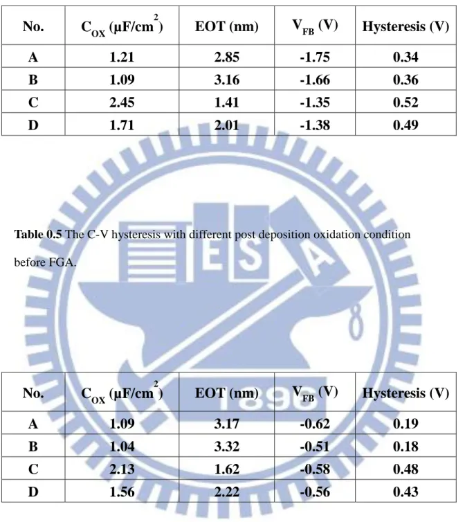
The oxide capacitance, EOT, flat band voltage and C-V hysteresis of all conditions are shown in Table 2.3, Table 2.4.
Although the interfacial layer GeO2 gave the low density of interface states and
high comprehensive performance, a large amount of fixed charge was introduced at the interface, which caused flat band voltage shifting that has not been systematically investigated yet [9]. High density fixed charges would cause lower mobility by strong coulomb scattering and shift of the threshold voltage.
The large C-V hysteresis is observed for our samples, more specifically for HfO2
gate stacks, is caused by bulk oxide traps and is not related to the passivation of the Ge interface [10].
Fig. 2.5 (a) shows the Ge 3d XPS spectra of Al2O3/GeOx/p-Ge with PDO 520 °C
30sec, PDO 520 °C 3min, PDO 550 °C 3min and RTO thermal GeO2 520 °C 30sec.
We can see that with an increase in the post deposition oxidation time or temperature, the GeOx peak become larger, which means the GeOx layer becomes thicker. This
peak energy is lower than the core level of Ge4+, indicating that the interfacial oxides
could include Ge suboxides. Fig. 2.5 (b) shows the deconvolution of GeOx peak to the
peak corresponding to each Ge oxidation state. We can see that with an increase in the post deposition oxidation time or temperature, the Ge3+peak become larger but the
Ge4+ peak remain the same. While the RTO thermal GeO2 520 °C 30sec sample has a
large Ge4+ peak, no significant components of lower oxidation states are detected.
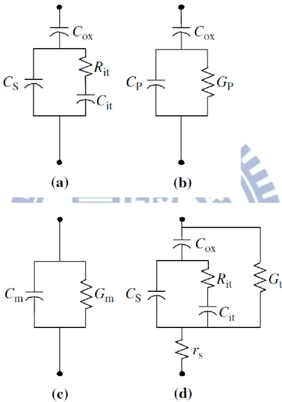
2.3.2 Conductance Method
The conductance method, proposed by Nicollian and Goetzberger in 1967, is one of the most sensitive methods to determine Dit [11]. It is the most complete method,
because it yields Dit in the depletion and weak inversion portion of the bandgap and
frequency capacitance methods could extract Dit, they will largely overestimate the Dit
value on Ge because of the humps caused by “minority carrier response” in the C-V curve. Conductance method is based on measuring the equivalent parallel
conductance GP of an MOSCAP as a function of bias voltage and frequency, the C-V
measurement applying gate bias a small sinusoidal voltage with frequency f and amplitude 25mV, the conductance is representing the loss mechanism due to interface trap capture and emission of carriers.
The simplified equivalent circuit of MOSCAP appropriate for the conductance method is shown in Fig. 2.6 (a). It consists of the oxide capacitance Cox , the
semiconductor capacitance CS, and the interface trap capacitance Cit . The circuit can
be simplified as in Fig. 2.6 (b), (2.1) (2.2) Where Cit = q2Dit ω = 2πf (f = measurement frequency) and τit = RitCit
The interface trap time constant, given by
(2.3)
Equations (2.1) and (2.2) are for interface traps with a single energy level in the bandgap. But in reality, interface trap are continuously distributed across the bandgap. Capture and emission occurs primarily by traps located within a few kT/q above and below the Fermi level, leading to a time constant dispersion and giving the normalized conductance as
(2.4)
From (2.2) and (2.4), conductance method is easier to extract Dit than capacitance
based method, because it does not require Cs. For (2.4), when GP/ω is plotted as a
function of ω, the maximum appears at ω ≈ 2/τit, and at that maximum
(2.5)
GP/ω plots are repeated at different gate voltage to determine Dit from the maximum
GP/ω and determine τit from ω at the peak conductance location on the ω-axis.
In the measurement, we assumed the device to consist of the parallel Cm − Gm
combination in Fig. 2.6 (c). The circuit gives GP/ω in terms of the measured
capacitance Cm, the oxide capacitance Cox, and the measured conductance Gm as
- (2.6)
According to τit
th e
E
kT , the interface trap time constant as a function of
temperature determines the part of interface traps in the bandgap observable in the MOS admittance characteristic. The traps located near to midgap could be observed at higher temperatures, while traps located near the band edges could be observed at lower temperature. And for small bandgap Ge, mid gap traps are able to be observed at room temperature. The behavior of the interface trap time constant at room
temperature as a function of capture cross section is shown in Fig. 2.7, which determines the part of interface traps in the bandgap observable in the MOS admittance characteristic. The electron thermal velocity, hole thermal velocity, effective density of states of conduction band (Nc) and effective density of states of
valence band (Nv) are all taken into account.
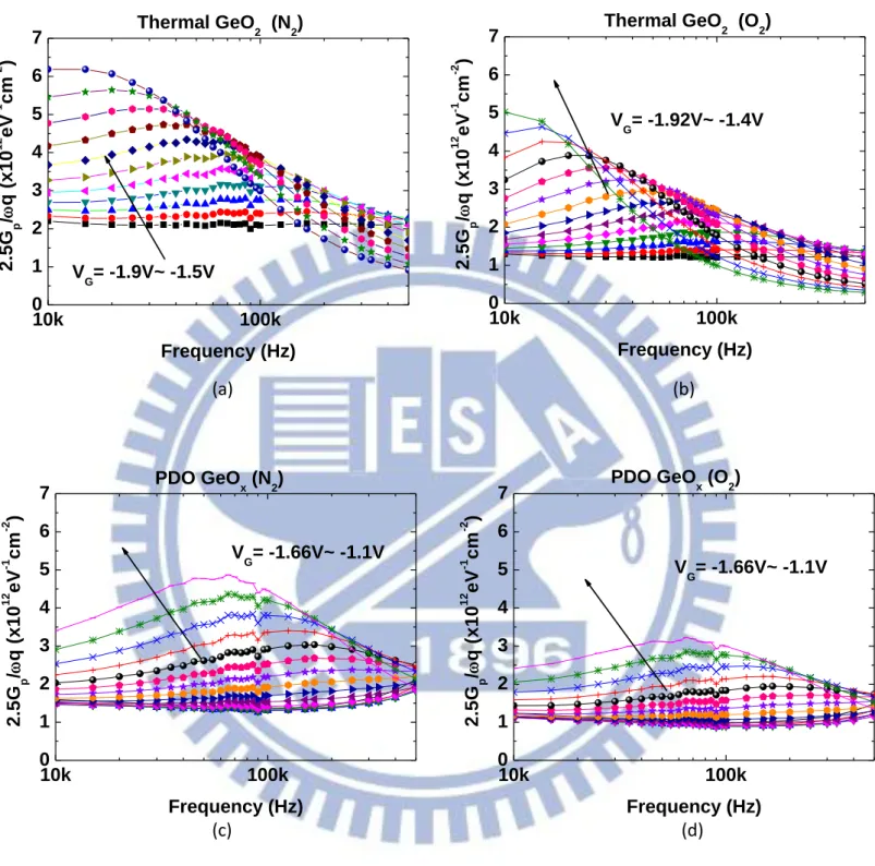
Fig. 2.8 shows the 2.5GP/ωq versus frequency of Ge MOSCAPs with different
different post deposition oxidation condition, and the measurement is performed at room temperature. The peak value of each 2.5GP/ωq curve equals to the interface state
density, and the frequency corresponding to the maximum 2.5GP/ωq can be converted
to energy in the bandgap by the equation . Therefore, the interface state density versus energy in the bandgap plots can be obtained by repeated at different gate voltages to scan trap energies.
The value of capture cross section is assumed to be around 10-16 cm2 in this
thesis. Dit profiles of each samples near midgap is shown in Fig. 2.10. We can see that
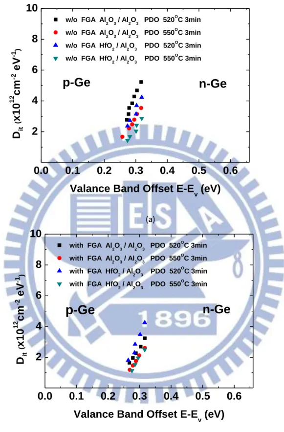
in Fig. 2.10 (a), the post oxidation deposition samples have less interface state density than RTO thermal GeO2, while we observed that Ge 3d XPS spectra of thermal GeO2
samples have large Ge4+ peak, which means it is not necessary to have a large Ge4+
peak to passivate high-k/Ge interface, the Ge3+ peak shows better interface quality
than Ge4+ peak in our studies. Also, the O2 PDA samples have less interface state
densitythan N2 PDA samples, we think the reason of less interface state density may
because of thicker GeOx grown after O2 PDA.
Fig. 2.10 (b) shows that the higher temperature of post deposition oxidation
samples have less interface state density than the lower temperature of post deposition oxidation samples. The Dit of GeOx/Ge MOS interface controlled by the GeOx
thickness has been studied [4]. We think the less interface state density is because of the thicker GeOx interfacial layer and larger Ge3+ peak which the higher post
deposition oxidation temperature grown.
The results shows more interface state density in the midgap, this phenomenon is called “weak inversion response” [12]. In the weak inversion regime, the C-V and conductance behavior becomes more complex, as shown in Fig. 2.11. In the weak inversion regime interface traps can communicate with both the majority and minority
carrier bands, as shown on the band diagram of Fig. 2.11 (a), due to the small
minority carrier time constant as the Fermi level located near midgap, the traps being filled and emptied by the ac voltage near the Fermi level can communicate with the minority band sufficiently fast and provide minority carriers to the band. When this dual communication occurs it leads to a larger conductance response than the typical depletion response.
The presence of the weak inversion response within the typical 1kHz to 1MHz measurement frequency window depends on the bandgap energy, the capture cross section and the temperature. For the Si/SiO2 interface this effect has been shown to be
present at lower frequencies at room temperature, not to occur in the 1kHz to 1MHz frequency window. But for small bandgap materials like germanium, the weak inversion response will be shown to be present in the 1kHz to 1MHz window. Therefore, conductance method for Ge MOSCAPs will overestimate the interface state density.
From the interface trap time constantτit
, the smaller bandgap material,
larger capture cross section and higher temperature lead weak inversion response more significant. Thus, the low temperature measurement can alleviate the dual communication.
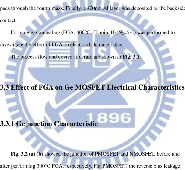
2.4 Effect of FGA on Electrical Characteristics
We employed low temperature 300°C forming gas annealing in a H2/N2 (5%) mixed
ambient for 30 minutes to improve the interface quality. Fig. 2.12 shows the multi frequency C-V of Ge MOSCAPs with different post deposition oxidation condition
after FGA, we can see that the hump becomes smaller in depletion region, and EOT is slightly larger.
The oxide capacitance, EOT, flat band voltage and C-V hysteresis with different post deposition oxidation condition before and after FGA are shown in Table 2.5 and
Table 2.6. The positive VFB shift and lower C-V hysteresis is shown in the samples
after FGA, we supposed that the positive VFB shift and lower C-V hysteresis is
because forming gas annealing lowering both fix charge and oxide trap charge. 2.5GP/ωq versus frequency of Ge MOSCAPs with different post deposition oxidation
condition after FGA is shown in Fig. 2.13, and the Dit profiles of each samples near
midgap, with and without FGA, is shown in Fig. 2.14. We can see that the Dit of all
samples are decreased after FGA, with a reduction of 16% to 44%, which means forming gas annealing could improve the high-k/Ge interface.
2.5 Conclusions
Ge PMOS capacitors using post deposition oxidation method to form a thin GeOx IL by oxidizing Ge surface beneath an ALD Al2O3 layer using high-k RTO was
fabricated, the dependence of the GeOx/Ge interface qualities on the post deposition
oxidation conditions such as post deposition oxidation temperature and post deposition annealing ambient was investigated. Theory of the conductance method was discussed in detail, including weak inversion response. The Ge 3d XPS spectra of Al2O3/GeOx/p-Ge with PDO 520 °C 30sec, PDO 520 °C 3min, PDO 550 °C 3min and
RTO thermal GeO2 520 °C 30sec is shown, the increase of post deposition oxidation
time or temperature will larger the Ge3+peak. The Ge3+ peak shows better interface
The EOT value was scaled down to 1.41 nm and a lower Dit value was obtained
by PDO. The larger EOT but lower Dit value was obtained by using O2 annealing. The
positive VFB shift and lower C-V hysteresis is shown in the samples after FGA, and
the Dit value has been reduced 16% ~ 44% after FGA. Finally, the HfO2/Al2O3 gate
stack with PDO 520°C 3min, PDA 500°C 60sec N2 was choose to be the best
References (Chapter 2)
[1] C. H. Huang, M. Y. Yang, A. Chin, W. J. Chen, C. X. Zhu, B. J. Cho, M.-F. Li, and D. L. Kwong, “ ery low defects and high performance
Ge-on-insulator p-MOSFETs with Al2O3 gate dielectrics,” in Symp. VLSI
Tech. Dig., pp. 119–120, 2003.
[2] W. P. Bai, N. Lu, J. Liu, A. Ramirez, D. L. Kwong, D. Wristers, A.Ritenour, L. Lee, and D. Antoniadis, “Ge MOS characteristics with CVD HfO gate dielectrics and Ta gate electrode,” in Symp. VLSI Tech. Dig., pp. 121–122, 2003.
[3] Y. Nakakita, R. Nakane, T. Sasada, H. Matsubara, M. Takenaka, and S. Takagi, “Interface-controlled self-align source/drain Ge pMOSFETs using thermally-oxidized GeO2 interfacial layers,” in IEDM Tech. Dig., pp.
877–880, 2008.
[4] R. Zhang, T. Iwasaki, N. Taoka, M. Takenaka, S. Takagi, “High-Mobility Ge pMOSFET With 1-nm EOT Al2O3/GeOx/Ge Gate Stack Fabricated by
Plasma Post Oxidation,” IEEE Trans Electron Devices, vol 59 , pp.335, 2012.
[5] R. Zhang, T. Iwasaki, N. Taoka,M. Takenaka, and S. Takagi, “Suppression of ALD-induced degradation of Ge MOS interface properties by low power plasma nitridation of GeO2,” in Proc. Ext. Abstr. SSDM, pp. 33–34, 2010.
[6] R. Zhang, T. Iwasaki, . Taoka, M. Takenaka, and S. Takagi, “Impact of GeOx interfacial layer thickness on Al2O3/Ge MOS interface properties,”
Microelectron. Eng., vol. 88, no. 7, pp. 1533–1536, Jul. 2011.
[7] G. V. Soares, C. Krug, L. Miotti, K. P. Bastos, G. Lucovsky, I. J. R. Baum, and C. Radtke, “Intermixing between HfO2 and GeO2 films deposited on Ge
(001) and Si (001): Role of the substrate,” Applied Physics Letters, vol 98, pp.131912 - 131912-3, 2011.
[8] T. Hosoi, K. Kutsuki, G. Okamoto, M. Saito, T. Shimura, and H.Watanabe, “Origin of flat band voltage shift and unusual minority carrier generation in thermally grown GeO2/Ge metal-oxide-semiconductor devices,” Appl Phys
Lett, vol 94, 2009.
[9] S. Deng, Q. Xie, D. Deduytsche, M. Schaekers, D. Lin, M. Caymax, A. Delabie, S. Van den Berghe, X. Qu, and C. Detavernier, "Effective reduction of fixed charge densities in germanium based metal-oxide-semiconductor devices," Appl. Phys. Lett., vol.99, pp. 052906, 2011.
[10] A. Delabie, F. Bellenger, M. Houssa, T. Conard, S. V. Elshocht, M. Caymax, M. Heyns, and M. Meuris, “Effective electrical passivation of Ge(100) for high-K gate dielectric layers using germanium oxide,” App. Phys. Lett., vol. 91, pp. 082 904, 2007.
[11] E.H. icollian and A. Goetzberger, “The Si–SiO2 Interface—Electrical Properties as Determined by the Metal-Insulator-Silicon Conductance Technique,” Bell Syst. Tech. J., vol 46, pp. 1055–1133, 1967.
[12] K. Martens, C. O. Chui, G. Brammertz, B. De Jaeger, D. Kuzum, M. Meuris, M. Heyns,T. Krishnamohan, K. Saraswat, H. E. Maes, G. Groeseneken, “On the correct extraction of interface trap density of MOS devices with high-mobility semiconductor substrates‖,” IEEE Trans. Elec. Dev.,55, pp. 547-555, Feb. 2008.
Fig. 0.2 The process flow and device structure with different post deposition oxidation
Table 0.1 The overview of a-d samples with different PDA condition.
No. ALD Al2O3 PDO ALD Al2O3 ALD HfO2 PDA
A 10cycles 520°C 3min 50cycles --- 500°C 60sec N2
B 10cycles 550°C 3min 50cycles --- 500°C 60sec N2
C 10cycles 520°C 3min --- 50cycles 500°C 60sec N2
D 10cycles 550°C 3min --- 50cycles 500°C 60sec N2
Table 0.2 The overview of A-D samples with different RTO condition. No. Thermal
GeO2
ALD Al
2O3 PDO ALD HfO2 PDA
a 520°C 30sec 10cycles --- 50cycles 500°C 60sec N2
b 520°C 30sec 10cycles --- 50cycles 500°C 60sec O2
c --- 10cycles 520°C 3min 50cycles 500°C 60sec N2
(a) (b)
(c) (d)
Fig. 0.3 The multi frequency C-V of Ge MOSCAPs with different PDA condition. (a)
RTO thermal GeO2 520°C 30sec with PDA 500°C 60sec N2 (b) RTO thermal GeO2
520°C 30sec with PDA 500°C 60sec O2 (c) post deposition oxidation 520°C 3min
with PDA 500°C 60sec N2 (d) post deposition oxidation 520°C 3min with PDA 500°C
60sec O2. -3 -2 -1 0 1 0.2 0.4 0.6 0.8 1.0 1.2 1.4 1.6 EOT = 2.97nm VFB = -2.26V C a p a c it a n c e ( F /c m 2 ) Voltage (V) 100KHz 10KHz 1KHz -3 -2 -1 0 1 0.2 0.4 0.6 0.8 1.0 1.2 1.4 1.6 C a p a c it a n c e ( F /c m 2 ) Voltage (V) 100KHz 10KHz 1KHz EOT = 2.58nm VFB = -2.37V -3 -2 -1 0 1 0.2 0.4 0.6 0.8 1.0 1.2 1.4 1.6 EOT = 2.12nm VFB = -1.69V C a p a c it a n c e ( F /c m 2 ) Voltage (V) 100KHz 10KHz 1KHz -3 -2 -1 0 1 0.2 0.4 0.6 0.8 1.0 1.2 1.4 1.6 EOT = 2.57nm VFB = -1.74V C a p a c it a n c e ( F /c m 2 ) Voltage (V) 100KHz 10KHz 1KHz
(a) (b)
(c) (d)
Fig. 0.4 The multi frequency C-V of Ge MOSCAPs with different post deposition
oxidation condition. (a) Al2O3/Al2O3 with post deposition oxidation GeO2 520°C 3min
(b) Al2O3/Al2O3 with post deposition oxidation GeO2 550°C 3min (c) HfO2/Al2O3
with post deposition oxidation GeO2 520°C 3min (d) HfO2/Al2O3 with post deposition
oxidation GeO2 550°C 3min.
-3 -2 -1 0 1 0.2 0.4 0.6 0.8 1.0 1.2 1.4 1.6 1.8 2.0 EOT = 2.85nm VFB = -1.75V C a p a c it a n c e ( F /c m 2 ) Voltage (V) 1MHz 100KHz 10KHz 1KHz -3 -2 -1 0 1 0.2 0.4 0.6 0.8 1.0 1.2 1.4 1.6 1.8 2.0 EOT = 3.16nm V FB = -1.66V C a p a c it a n c e ( F /c m 2 ) Voltage (V) 1MHz 100KHz 10KHz 1KHz -3 -2 -1 0 1 0.2 0.4 0.6 0.8 1.0 1.2 1.4 1.6 1.8 2.0 EOT = 1.41nm VFB = -1.35V C a p a c it a n c e ( F /c m 2 ) Voltage (V) 1MHz 100KHz 10KHz 1KHz -3 -2 -1 0 1 0.2 0.4 0.6 0.8 1.0 1.2 1.4 1.6 1.8 2.0 EOT = 2.01nm VFB = -1.38V C a p a c it a n c e ( F /c m 2 ) Voltage (V) 1MHz 100KHz 10KHz 1KHz
Table 0.3 The C-V hysteresis with different PDA condition.
Table 0.4 The C-V hysteresis with different post deposition oxidation condition.
No.
C
OX(µF/cm
2)
EOT (nm)
V
FB(V)
Hysteresis (V)
a
1.34
2.58
-2.37
0.73
b
1.16
2.97
-2.26
0.7
c
1.63
2.12
-1.69
0.69
d
1.34
2.57
-1.74
0.7
No.
C
OX(µF/cm
2)
EOT (nm)
V
FB(V)
Hysteresis (V)
A
1.21
2.85
-1.75
0.34
B
1.09
3.16
-1.66
0.36
C
2.45
1.41
-1.35
0.52
(a)
(b)
Fig. 0.5 The XPS spectra of Al2O3/GeOx/p-Ge with different PDO and thermal grown
GeOx condition.
36
34
32
30
28
Ge0 Ge1+ Ge2+ Ge3+ PDO 520o C 30secIn
te
n
s
it
y
(
a
.u
.)
Ge4+ PDO 520oC 3min PDO 550oC 3min Thermal 520oC 30secBinding Energy (eV)
36
34
32
30
28
GeO
xGe
4+Ge
0Ge 3
d
Binding Energy (eV)
In
te
n
s
it
y
(
a
.u
.)
PDO 520oC 30sec PDO 520oC 3min PDO 550oC 3min Thermal 520oC 30secFig. 0.6 Equivalent circuits for conductance measurements; (a) MOSCAP with
interface trap time constant τit = RitCit , (b) simplified circuit of (a), (c) measured
Fig. 0.7 The behavior of the interface trap time constant at room temperature as a
function of capture cross section determines the part of interface traps in the bandgap observable in the MOS admittance characteristic.
0.0
0.1
0.2
0.3
0.4
0.5
0.6
10
210
310
410
510
610
710
810
910
1010
1110
12 =1E-15cm2 =1E-16cm2 =1E-17cm2n-Ge
p-Ge
In
te
rf
a
c
e
T
ra
p
F
re
q
u
e
n
c
y
(
H
z
)
Valance Band Offset E-E
v(eV)
(a) (b)
(c) (d)
Fig. 0.8 2.5GP/ωq versus frequency of Ge MOSCAPs with different PDA condition.
(a) RTO thermal GeO2 520°C 30sec with PDA 500°C 60sec N2 (b) RTO thermal GeO2
520°C 30sec with PDA 500°C 60sec O2 (c) post deposition oxidation 520°C 3min
with PDA 500°C 60sec N2 (d) post deposition oxidation 520°C 3min with PDA 500°C
60sec O2. 10k 100k 0 1 2 3 4 5 6 7 VG= -1.9V~ -1.5V 2 .5 G p / q (x10 12 eV -1 cm -2 ) Frequency (Hz) Thermal GeO2 (N2) 10k 100k 0 1 2 3 4 5 6 7 Thermal GeO2 (O2) VG= -1.92V~ -1.4V 2 .5 G p / q (x10 12 eV -1 cm -2 ) Frequency (Hz) 10k 100k 0 1 2 3 4 5 6 7 PDO GeOx (N2) VG= -1.66V~ -1.1V 2 .5 G p / q (x10 12 eV -1 cm -2 ) Frequency (Hz) 10k 100k 0 1 2 3 4 5 6 7 PDO GeOx (O2) VG= -1.66V~ -1.1V 2 .5 G p / q (x10 12 eV -1 cm -2 ) Frequency (Hz)
(A) (B)
(C) (D)
Fig. 0.9 2.5GP/ωq versus frequency of Ge MOSCAPs with different post deposition
oxidation condition. (A) Al2O3/Al2O3 with post deposition oxidation GeO2 520°C
3min (B) Al2O3/Al2O3 with post deposition oxidation GeO2 550°C 3min (C)
HfO2/Al2O3 with post deposition oxidation GeO2 520°C 3min (D) HfO2/Al2O3 with
post deposition oxidation GeO2 550°C 3min.
1k 10k 100k 1M 0.0 2.0x10¹² 4.0x10¹² 6.0x10¹² 8.0x10¹² 1.0x10¹³ 1.2x10¹³ VG= -1.3V~ -0.6V 2 .5 G p / q (eV -1 cm -2 ) Frequency(Hz) 1k 10k 100k 1M 0.0 2.0x10¹² 4.0x10¹² 6.0x10¹² 8.0x10¹² 1.0x10¹³ 1.2x10¹³ V G= -1.3V~ -0.6V 2 .5 G p / q (eV -1 cm -2 ) Frequency(Hz) 1k 10k 100k 1M 0.0 2.0x10¹² 4.0x10¹² 6.0x10¹² 8.0x10¹² 1.0x10¹³ 1.2x10¹³ VG= -1.4V~ -0.7V 2 .5 G p / q (eV -1 cm -2 ) Frequency(Hz) 1k 10k 100k 1M 0.0 2.0x10¹² 4.0x10¹² 6.0x10¹² 8.0x10¹² 1.0x10¹³ 1.2x10¹³ V G= -1.4V~ -0.7V 2 .5 G p / q (eV -1 cm -2 ) Frequency(Hz)
(a)
(b)
Fig. 0.10 Dit profiles of each samples near midgap (a) samples a b c d and (b) samples
A B C D.
0.0
0.1
0.2
0.3
0.4
0.5
0.6
2
4
6
8
10
n-Ge
p-Ge
w/o FGA Al 2O3 / Al2O3 PDO 520 O C 3minw/o FGA Al2O3 / Al2O3 PDO 550OC 3min
w/o FGA HfO2 / Al2O3 PDO 520OC 3min
w/o FGA HfO
2 / Al2O3 PDO 550 O C 3min
D
it (x10
12cm
-2e
V
-1 )Valance Band Offset E-E
v
(eV)
0.0
0.1
0.2
0.3
0.4
0.5
0.6
2
4
6
8
10
n-Ge
p-Ge
D
itdistribution in Ge Band Gap
RTO GeO 2 PDA N2 RTO GeO 2 PDA O2 PDO GeO 2 PDA N2 PDO GeO 2 PDA O2
D
it(
x10
12cm
-2e
V
-1 )Valance Band Offset E-E
(a) (b)
(c)
Fig. 0.11 A band diagram showing the weak inversion response (a) and the general
equivalent circuits used to model the MOS capacitor C-V and G-V characteristics across the bandgap for an n-type capacitor. The first circuit (b) models one trap only: Cox is the oxide capacitance, Cinv the inversion capacitance, Cdep the depletion (and
accumulation) capacitance, CT the trap capacitance and Gn and Gp electron and hole
(a) (b)
(c) (d)
Fig. 0.12 The multi frequency C-V of Ge MOSCAPs with different post deposition
oxidation condition after FGA. (a) Al2O3/Al2O3 with post deposition oxidation GeO2
520°C 3min (b) Al2O3/Al2O3 with post deposition oxidation GeO2 550°C 3min (c)
HfO2/Al2O3 with post deposition oxidation GeO2 520°C 3min (d) HfO2/Al2O3 with
post deposition oxidation GeO2 550°C 3min.
-2 -1 0 1 2 0.2 0.4 0.6 0.8 1.0 1.2 1.4 1.6 1.8 EOT = 3.17nm V FB = -0.62V C a p a c it a n c e ( F /c m 2 ) Voltage (V) 1MHz 100KHz 10KHz 1KHz -2 -1 0 1 2 0.2 0.4 0.6 0.8 1.0 1.2 1.4 1.6 1.8 EOT = 3.32nm V FB = -0.51V C a p a c it a n c e ( F /c m 2 ) Voltage (V) 1MHz 100KHz 10KHz 1KHz -2 -1 0 1 2 0.2 0.4 0.6 0.8 1.0 1.2 1.4 1.6 1.8 EOT = 1.62nm VFB = -0.58V C a p a c it a n c e ( F /c m 2 ) Voltage (V) 1MHz 100KHz 10KHz 1KHz -2 -1 0 1 2 0.2 0.4 0.6 0.8 1.0 1.2 1.4 1.6 1.8 EOT = 2.22nm VFB = -0.56V C a p a c it a n c e ( F /c m 2 ) Voltage (V) 1MHz 100KHz 10KHz 1KHz
Table 0.5 The C-V hysteresis with different post deposition oxidation condition
before FGA.
Table 0.6 The C-V hysteresis with different post deposition oxidation condition after
FGA.
No.
C
OX(µF/cm
2)
EOT (nm)
V
FB(V)
Hysteresis (V)
A
1.21
2.85
-1.75
0.34
B
1.09
3.16
-1.66
0.36
C
2.45
1.41
-1.35
0.52
D
1.71
2.01
-1.38
0.49
No.
C
OX(µF/cm
2)
EOT (nm)
V
FB(V)
Hysteresis (V)
A
1.09
3.17
-0.62
0.19
B
1.04
3.32
-0.51
0.18
C
2.13
1.62
-0.58
0.48
(a) (b)
(c) (d)
Fig. 0.13 2.5GP/ωq versus frequency of Ge MOSCAPs with different post deposition
oxidation condition after FGA. (a) Al2O3/Al2O3 with post deposition oxidation GeO2
520°C 3min (b) Al2O3/Al2O3 with post deposition oxidation GeO2 550°C 3min (c)
HfO2/Al2O3 with post deposition oxidation GeO2 520°C 3min (d) HfO2/Al2O3 with
post deposition oxidation GeO2 550°C 3min.
1k 10k 100k 1M 0.0 2.0x10¹² 4.0x10¹² 6.0x10¹² 8.0x10¹² 1.0x10¹³ VG=0.2V~0.6V 2 .5 G p / q (eV -1 cm -2 ) Frequency(Hz) 1k 10k 100k 1M 0.0 2.0x10¹² 4.0x10¹² 6.0x10¹² 8.0x10¹² 1.0x10¹³ VG=0.2V~0.6V 2 .5 G p / q (eV -1 cm -2 ) Frequency(Hz) 1k 10k 100k 1M 0.0 2.0x10¹² 4.0x10¹² 6.0x10¹² 8.0x10¹² 1.0x10¹³ VG= -0.3V~0.2V 2 .5 G p / q (eV -1 cm -2 ) Frequency(Hz) 1k 10k 100k 1M 0.0 2.0x10¹² 4.0x10¹² 6.0x10¹² 8.0x10¹² 1.0x10¹³ V G= -0.3V~0.1V 2 .5 G p / q (eV -1 cm -2 ) Frequency(Hz)
(a)
(b)
Fig. 0.14 Dit profiles of each samples near midgap (a) samples A B C D without FGA
(b) samples A B C D with FGA.
0.0
0.1
0.2
0.3
0.4
0.5
0.6
2
4
6
8
10
n-Ge
p-Ge
w/o FGA Al 2O3 / Al2O3 PDO 520 O C 3min w/o FGA Al2O 3 / Al2O3 PDO 550 O C 3minw/o FGA HfO2 / Al
2O3 PDO 520
O
C 3min
w/o FGA HfO
2 / Al2O3 PDO 550 O C 3min
D
it (x10
12cm
-2e
V
-1 )Valance Band Offset E-E
v
(eV)
0.0
0.1
0.2
0.3
0.4
0.5
0.6
2
4
6
8
10
p-Ge
n-Ge
with FGA Al 2O3 / Al2O3 PDO 520 O C 3min with FGA Al2O 3 / Al2O3 PDO 550 O C 3minwith FGA HfO
2 / Al2O3 PDO 520
O
C 3min
with FGA HfO2 / Al
2O3 PDO 550 O C 3min
D
it (x10
12cm
-2e
V
-1 )Valance Band Offset E-E
Chapter 3
Germanium MOSFET with
Atomic-Layer-Deposited HfO
2/Al
2O
3/GeO
x/Ge
Gate Stack Fabricated by Post deposition
oxidation
3.1 Introduction
Recently, it has been increasingly difficult to further improve the performances of Si complementary metal–oxide–semiconductor (CMOS) devices through the conventional device scaling [1]. To keep up with the performance growth which indicated by the ITRS roadmap[2], device engineers need to introduce more and more new materials [3], the high mobility semiconductor materials received interest in MOSFET applications to pursue much higher device performance. Germanium is an attractive candidate for channel material due to its high electron/hole mobility and the compatibility with the conventional Si integration technologies.
However, a major problem which has retarded scaling of Ge devices is interface passivation,unlike SiO2 with a highly thermal stability, Ge native oxides are water
soluble and thermal instable, it is difficult to achieve a high-quality oxide/Ge interface due to the bad surface properties of Ge. Another problem is Ge has a smaller bandgap than conventional Si substrate, which resulting in higher junction leakage currents.
![HPSH [ 氧化數平衡反應式係數 ]](data:image/gif;base64,R0lGODlhAQABAIAAAP///wAAACH5BAEAAAAALAAAAAABAAEAAAICRAEAOw==)