極高速快閃式類比數位轉換器
96
0
0
全文
(2) 極高速快閃式類比數位轉換器 Ultra High-Speed Flash Analog-to-Digital Converter 研 究 生:徐瑛佑. Student : Ying-Yu Hsu. 指導教授:蘇朝琴 教授. Advisor : Chau-Chin Su. 國 立 交 通 大 學 電機與控制工程研究所 碩士論文. A Thesis Submitted to Department of Electrical and Control Engineering College of Electrical Engineering and Computer Science National Chiao Tung University in partial Fulfillment of the Requirements for the Degree of Master in Electrical and Control Engineering July 2005 Hsinchu, Taiwan, Republic of China. 中華民國九十四年七月.
(3) 極高速快閃式類比數位轉換器. 研究生 : 徐瑛佑. 指導教授 : 蘇朝琴 教授. 國立交通大學電機與控制工程研究所. 摘. 要. 由於製程技術的進步,CMOS 積體電路的操作頻率及電路複雜度也隨著增加。介於類 比與數位之間的介面需要極高速的操作速度,約是每秒幾百萬次取樣到每秒幾億次取樣不 等。這些高傳輸率的系統,包含 DVD 讀取通道、多準位接收器、通道等畫器、時脈抖動量 測系統或乙太網路都需要類比數位轉換器。 在這篇論文中包含了兩個主題。首先,我們將焦點放在高速類比數位轉換器的電路設 計方法,因此我們提出一個在一般能操作於每秒 31.25 億次取樣,最高可操作於每秒 40 億 次取樣的 4 位元快閃式類比數位轉換器,這個 4 位元快閃式類比數位轉換器在輸入頻率高 達每秒 15.5 億時用每秒 31.25 億次取樣的情況下能有超過 3.1 的有效位元,而在輸入頻率高 達每秒 20 億時用每秒 40 億次取樣的情況下能有超過 2.3 的有效位元。它的最大差分非線性 誤差與積分非線性誤差分別小於 0.45 與 0.6 最小位元。這個類比數位轉換器操作於 1.8 伏特 的電源供應且每秒 40 億次取樣時消耗 180 毫瓦,這晶片使用 TSMC 0.18-um 1P6M CMOS 實做時佔了 0.36- mm 2 的面積。 接著,我們根據 4 位元快閃式類比數位轉換器的電路,我們提出了兩個方法使得 4 位 元的精準度提高到 5 位元的精準度。這兩個方法分別是主動式平均技巧與主動式內插技巧, 使用主動式平均技巧可以得到較高的精準度,但使用主動式內插技巧卻可以節省較多的功 率消耗。這個使用了主動式平均技巧的 5 位元快閃式類比數位轉換器在輸入頻率高達每秒 15.5 億時用每秒 31.25 億次取樣的情況下能有超過 3.8 的有效位元,而在輸入頻率高達每秒.
(4) 20 億時用每秒 40 億次取樣的情況下能有超過 3 的有效位元。它的最大差分非線性誤差與積 分非線性誤差分別小於 0.35 與 0.8 最小位元。這個類比數位轉換器操作於 1.8 伏特的電源供 應且每秒 4 億次取樣時消耗 270 毫瓦。這個使用了主動式內插技巧的 5 位元快閃式類比數 位轉換器在輸入頻率高達每秒 15.5 億時用每秒 31.25 億次取樣的情況下能有超過 3.6 的有效 位元,而在輸入頻率高達每秒 20 億時用每秒 40 億次取樣的情況下能有超過 2.9 的有效位 元。它的最大差分非線性誤差與積分非線性誤差分別小於 0.5 與 0.9 最小位元。這個類比數 位轉換器操作於 1.8 伏特的電源供應且每秒 4 億次取樣時消耗 243 毫瓦。 關鍵字:類比數位轉換器,快閃式轉換器,追蹤與保持電路,前置放大器,比較器, 葛雷碼,平均,內插。.
(5) Ultra High-Speed Flash Analog-to-Digital Converter. Student: Ying-Yu Hsu. Advisor: Chau-Chin Su. Institute of Electrical and Control Engineering National Chiao Tung University. Abstract Due to the advance process technologies, the operating frequency and circuit complexity of integrated circuit increase. The interfaces between the analog and the digital parts are required to operate at ultra high speed (over giga samples per second). The high-bit-rate applications include DVD read channel, multi level receiver, channel equalizer, jitter measurement system, and Ethernet need Analog-to-Digital Converters. There are two major topics in this thesis. First, we focus on the high speed ADC circuit design. Thus, we propose a 4-bit flash ADC typically operates at 3.125GSps and maximally at 4GSps. This 4-bit ADC achieves better than 3.1 effective bits for input frequencies up to 1.55GHz at 3.125GSps, and 2.3 effective bits for 2GHz input at 4GSps. The peak DNL and INL are less than 0.45 LSB and 0.6 LSB, respectively. This ADC consumes 180mW from 1.8V power supply at 4GSps. The chip occupies 0.36- mm 2 active area, implemented in TSMC 0.18-um 1P6M CMOS..
(6) Second, based on the circuits presented in the 4-bit flash ADC, and we propose two methods to improve the 4-bit accuracy to 5-bit accuracy. The methods are active averaging and active interpolation techniques. Using averaging technique can improve accuracy white using interpolation technique can reduce power consumption. The 5-bit flash ADC with averaging technique achieves better than 3.8 effective bits for input frequencies up to 1.55GHz at 3.125GSps, and 3 effective bits for 2GHz input at 4GSps. The peak DNL and INL are less than 0.35 LSB and 0.8 LSB, respectively. This ADC consumes 270mW from 1.8V power supply at 4GSps. The 5-bit flash ADC with interpolation technique achieves better than 3.6 effective bits for input frequencies up to 1.55GHz at 3.125GSps, and 2.9 effective bits for 2GHz input at 4GSps. The peak DNL and INL are less than 0.5 LSB and 0.9 LSB, respectively. This ADC consumes 243mW from 1.8V power supply at 4GSps. Index Terms: Analog-to-Digital Converter, Flash Converter, Track-and-Hold, Preamplifier, Comparator, Gray Code, Averaging, Interpolation..
(7) 誌. 謝. 無論在這兩年的研究所求學生涯或未來職涯發展上,最感謝的是我的指導老師 蘇朝琴 教授,人說讀萬卷書不如行萬里路,我說行萬里路又不如覓得一位良師。能拜於蘇老師門 下,實為我一生中莫大福緣,由衷之言何足道哉,祝老師身體健康、萬事如意。 再者,感謝陪我一路走來的實驗室學長、同學及學弟們,你們的陪伴豐富了我這兩年 的人生回憶,衷心的祝福各位研究順遂、鵬程似錦。還有我大學的好朋友及來到新竹後認 識的新朋友,謝謝你們的支持與陪伴,陪我度過無數歡樂或失意的日子。 最後,我要將這份喜悅與我的家人一同分享,尤其是我親愛的母親,沒有您無悔的付 出,或許永遠也沒有機會完成學業,這個學位應該是頒給您的,我愛您,母親!. 徐 瑛 佑 2005/7/27.
(8) Table of Contents CHAPTER 1. INTRODUCTION..........................................................1. 1.1 MOTIVATION ........................................................................................................................................................ 1 1.2 THESIS ORGANIZATION ........................................................................................................................................ 2. CHAPTER 2 REVIEW OF HIGH SPEED CMOS ADC ARCHITECTURES ....................................................................................................................4 2.1 FULL FLASH ADC ............................................................................................................................................... 4 2.2 INTERPOLATING ADC.......................................................................................................................................... 6 2.3 TIME INTERLEAVED ADC [8]............................................................................................................................... 8 2.4 PIPELINED ADC................................................................................................................................................. 10 2.5 FOLDING ADC [9] ............................................................................................................................................. 11. CHAPTER 3. DESIGN TECHNIQUES OF FLASH ADC ..............13. 3.1 AVERAGING TECHNIQUE .................................................................................................................................... 13 3.1.1 Resistive Averaging................................................................................................................................... 14 3.1.2 Active Averaging ....................................................................................................................................... 15 3.2 INTERPOLATION ................................................................................................................................................. 16 3.2.1 Resistive Interpolation .............................................................................................................................. 16 3.2.2 Active Interpolation .................................................................................................................................. 17 3.3 COMPARISON OF DIFFERENT DESIGN TECHNIQUES............................................................................................ 18 3.3.1 6-bit Flash ADC with Auto-zero Technique [12] ...................................................................................... 18 3.3.2 6-bit Flash ADC with Sample-and-Hold and Auto-zero Technique [13] .................................................. 19 3.3.3 6-bit Flash ADC with Background Digital Calibration [14].................................................................... 20 3.3.4 6-bit Flash ADC with Distributed T/Hs and Resistive Interpolation [15][16] ......................................... 22 3.3.5 6-bit Flash ADC with Resistive Averaging [17] ....................................................................................... 23 3.4 DESIGN ISSUES AND ARCHITECTURE OF ULTRA HIGH SPEED FLASH ADC ........................................................ 25 3.4.1 Design Guidelines..................................................................................................................................... 25 3.4.2 4-bit 4-GSps Flash Architecture ............................................................................................................... 26 3.4.3 5-bit 4-GSps Flash Architecture Using Active Averaging Technique........................................................ 27 3.4.4 5-bit 4-GSps Flash Architecture Using Active Interpolation Technique ................................................... 29 ................................................................................................................................................................................ 30. CHAPTER 4. A 4-BIT 4 GSPS FLASH ADC CIRCUIT DESIGN .31. 4.1 FRONT-END TRACK-AND-HOLD ........................................................................................................................ 31 4.2 PREAMPLIFIER ................................................................................................................................................... 38.
(9) 4.3 FIRST LATCH ..................................................................................................................................................... 41 4.4 SECOND LATCH ................................................................................................................................................. 43 4.5 DIGITAL ENCODER ............................................................................................................................................. 44 4.6 CLOCK GENERATOR AND OUTPUT DRIVER ........................................................................................................ 48 4.7 WHOLE CHIP DESIGN ISSUES ............................................................................................................................. 50 4.8 SUMMARY ......................................................................................................................................................... 52. CHAPTER 5. A 5-BIT 4 GSPS FLASH ADC CIRCUIT DESIGN .53. 5.1 PREAMPLIFIER ................................................................................................................................................... 53 5.2 AVERAGING ....................................................................................................................................................... 57 5.3 INTERPOLATION ................................................................................................................................................. 59 5.4 SUMMARY ......................................................................................................................................................... 61. CHAPTER 6. SIMULATION RESULTS...........................................62. 6.1 CIRCUITS SIMULATION ...................................................................................................................................... 62 6.1.1 Track-and-Hold Simulation ...................................................................................................................... 62 6.1.2 Preamplifier Simulation............................................................................................................................ 66 6.1.3 Comparator Simulation ............................................................................................................................ 69 6.2 STATIC PERFORMANCE SIMULATION .................................................................................................................. 70 6.3 DYNAMIC PERFORMANCE SIMULATION ............................................................................................................. 74 6.4 SUMMARY ......................................................................................................................................................... 78. CHAPTER 7. CONCLUSION ............................................................79. BIBLIOGRAPHY...................................................................................81.
(10) List of Figures FIGURE 2.1 FULL FLASH ADC ARCHITECTURE. .............................................................................................................. 5 FIGURE 2.2 INTERPOLATING ADC ARCHITECTURE. ........................................................................................................ 6 FIGURE 2.3 TIME INTERLEAVED ADC ARCHITECTURE AND TIMING. ............................................................................... 8 FIGURE 2.4 SPECTRUM OF A RECONSTRUCTED SINUSOID FOR A FOUR-WAY CONVERTER ARRAY. ..................................... 9 FIGURE 2.5 PIPELINED ADC ARCHITECTURE................................................................................................................ 10 FIGURE 2.6 FOLDING ADC ARCHITECTURE AND THE TRANSFER CURVE OF A FOLDING CIRCUIT IN COMPARISON WITH THE FULL FLASH ADC. ....................................................................................................................................... 11. FIGURE 3.1RESISTIVE AVERAGING SCHEME [11] .......................................................................................................... 14 FIGURE 3.2 ACTIVE AVERAGING SCHEME ..................................................................................................................... 15 FIGURE 3.3 RESISTIVE INTERPOLATION SCHEME .......................................................................................................... 16 FIGURE 3.4 ACTIVE INTERPOLATION SCHEME ............................................................................................................... 17 FIGURE 3.5 6-BIT FLASH ADC WITH AUTO-ZERO TECHNIQUE ....................................................................................... 18 FIGURE 3.6 6-BIT FLASH ADC WITH S/H AND AUTO-ZERO TECHNIQUE ........................................................................ 20 FIGURE 3.7 6-BIT FLASH ADC WITH BACKGROUND DIGITAL CALIBRATION .................................................................. 21 FIGURE 3.8 6-BIT FLASH ADC WITH DISTRIBUTED T/H AND RESISTIVE INTERPOLATION .............................................. 22 FIGURE 3.9 6-BIT FLASH ADC WITH RESISTIVE AVERAGING ......................................................................................... 24 FIGURE 3.10 4-BIT FLASH ADC ARCHITECTURE ........................................................................................................... 26 FIGURE 3.11 5-BIT FLASH ADC WITH ACTIVE AVERAGING TECHNIQUE ......................................................................... 28 FIGURE 3.12 5-BIT FLASH ADC WITH ACTIVE INTERPOLATION TECHNIQUE .................................................................. 30 FIGURE 4.1 TRACK-AND-HOLD IN OPEN LOOP CONFIGURATION ................................................................................... 32 FIGURE 4.2 PSEUDO-DIFFERENTIAL TYPE TRACK-AND-HOLD IN OPEN LOOP CONFIGURATION ..................................... 32 FIGURE 4.3 TRACK-AND-HOLD WITH PMOS CONSTANT CURRENT SOURCE................................................................. 33 FIGURE 4.4 PMOS PUSH-PULL SOURCE FOLLOWER BUFFER ......................................................................................... 34 FIGURE 4.5 (A) NMOS CONSTANT CURRENT SOURCE FOLLOWER, (B) NMOS PUSH-PULL SOURCE FOLLOWER (C) NMOS CONSTANT CURRENT & PUSH-PULL SOURCE FOLLOWER ......................................................................... 35 FIGURE 4.6 NEW PSEUDO-DIFFERENTIAL ARCHITECTURE ............................................................................................ 36 FIGURE 4.8 OPEN-LOOP SINGLE-POLE AMPLIFIER ......................................................................................................... 38 FIGURE 4.9 STEP-INPUT RESPONSE OF PREAMPLIFIER ................................................................................................... 39 FIGURE 4.10 FULLY DIFFERENTIAL OPEN-LOOP SINGLE-POLE PREAMPLIFIER ............................................................... 40 FIGURE 4.11 FIRST LATCH CIRCUIT .............................................................................................................................. 41 FIGURE 4.12 TWO FIRST LATCH OPERATION MODE, (A) RESET MODE, (B) REGENERATION MODE ................................. 42 FIGURE 4.13 SECOND LATCH CIRCUIT .......................................................................................................................... 43 FIGURE 4.14 DIGITAL ENCODER ................................................................................................................................... 46 FIGURE 4.16 CLOCK GENERATOR ................................................................................................................................. 48.
(11) FIGURE 4.17 OPEN-DRAIN OUTPUT DRIVER .................................................................................................................. 49 FIGURE 4.18 LAYOUT FLOORPLAN ............................................................................................................................... 50 FIGURE 4.19 LAYOUT OF THE 4-BIT 4GSPS FLASH ADC .............................................................................................. 51 FIGURE 5.1 (A) DIFFERENTIAL PAIR WITH DIODE-CONNECTED PMOS AND (B) ADDING CURRENT SOURCES TO INCREASE THE VOLTAGE GAIN ............................................................................................................................................. 54. FIGURE 5.2 LOW KICK BACK NOISE COMPARATOR CIRCUIT DIAGRAM .......................................................................... 55 FIGURE 5.3 FOUR-WAY INPUT PREAMPLIFIER WITH RESET LATCH ................................................................................ 56 FIGURE 5.4 ACTIVE AVERAGING METHOD OF PREAMPLIFIERS....................................................................................... 58 FIGURE 5.5 ACTIVE INTERPOLATION METHOD OF PREAMPLIFIERS ................................................................................ 60 FIGURE 6.1 POSITIVE AND NEGATIVE SLEW RATE OF THREE TYPE BUFFERS ................................................................. 63 FIGURE 6.2 LINEARITY PERFORMANCE OF THREE TYPE BUFFERS ................................................................................. 64 FIGURE 6.3 DYNAMIC PERFORMANCE OF T/H AT 498MHZ INPUT SIGNAL ................................................................... 65 FIGURE 6.4 DYNAMIC PERFORMANCE OF T/H AT 3.125GSPS AND 4GSPS .................................................................... 65 FIGURE 6.5 FREQUENCY RESPONSE OF THE PASSIVE LOAD PREAMPLIFIER .................................................................... 66 FIGURE 6.6 PREAMPLIFIER INPUT-REFERRED OFFSET DISTRIBUTION ............................................................................ 68 FIGURE 6.7 SPEED PERFORMANCE OF THE COMPARATOR .............................................................................................. 69 FIGURE 6.8 DNL AND INL OF THE 4-BIT ADC AT 4GSPS.............................................................................................. 70 FIGURE 6.9 DNL AND INL OF THE 5-BIT ADC AT 4GSPS WITH AVERAGING TECHNIQUE............................................... 71 FIGURE 6.10 DNL AND INL OF THE 5-BIT ADC AT 4GSPS WITH INTERPOLATION TECHNIQUE ...................................... 72 FIGURE 6.11 POST-SIMULATION OF DNL AND INL OF THE 4-BIT ADC AT 4GSPS WITHOUT MISMATCH ........................ 73 FIGURE 6.12 ENOB OF THE 4-BIT ADC AT 3.125GSPS AND 4GSPS .............................................................................. 74 FIGURE 6.13 ENOB OF THE 5-BIT ADC WITH AVERAGING TECHNIQUE AT 3.125GSPS AND 4GSPS ............................... 74 FIGURE 6.14 ENOB OF THE 5-BIT ADC WITH INTERPOLATION TECHNIQUE AT 3.125GSPS AND 4GSPS ........................ 75 FIGURE 6.15 DYNAMIC PERFORMANCE OF PRE-SIMULATION OF THE 4-BIT ADC AT 3.125GSPS AND 1.55GHZ INPUT SIGNAL. .............................................................................................................................................................. 76. FIGURE 6.16 DYNAMIC PERFORMANCE OF POST-SIMULATION OF THE 4-BIT ADC AT 3.125GSPS AND 1.55GHZ INPUT SIGNAL. .............................................................................................................................................................. 77.
(12) List of Tables TABLE 4-1 BINARY-GRAY-THERMOMETER CODE IMPLEMENTATION............................................................................ 45 TABLE 6-1 MISMATCH PARAMETERS FOR SEVERAL CMOS TECHNIQUE ....................................................................... 67 TABLE 6-2 PERFORMANCE SUMMARY .......................................................................................................................... 78 TABLE 7-1 ADC PERFORMANCE COMPARISON ............................................................................................................. 80.
(13) Chapter 1. Chapter 1 Introduction. 1.1. Motivation In recent years, the increasing versatility of digital signal processing in. communication applications, digital receivers are required for high-bit-rate communication systems. It requires high speed interface between the analog and the digital domains. Such interface converts analog signals into digital form at the speed over giga samples per second. The wide proliferation of the digital signal processing across large and diverse sets of applications has made analog-to-digital converter a key functional interface integrated. in. most. analog/digital. VLSI. systems.. The. requirements. of. analog-to-digital converter, which are applied to various applications, are different. These high-bit-rate communication systems such as PRML read channel, Gigabit Ethernet, multi level receiver and jitter measurement system do not require high resolution but high speed. For determining the topology of a high speed ADC, several existing architectures are studied and reviewed. According to the different requirements in high-bit-rate communication systems, the requirements of the flash ADC are also different. For example, the hard disc or DVD read channel need 6-bit resolution but only several hundred MSps to 1~2 GSps. The multi level receiver, channel equalizer or jitter measurement system need ultra high speed for many GSps with only 3~4 bit resolution. Systems such as 1.
(14) Chapter 1 optical receivers need 5-bit resolution and at more then 10 GSps. These ultra high speed ADC are often developed in SiGe BiCMOS or GaAs HBT technology [1][2][3]. Or, they are integrated with several parallel CMOS ADC channels and implemented in a time-interleaved sampling technique [4][5][6][7]. Relatively, the circuit requires larger chip size and power dissipation In resent years, the trends of flash ADC design are on the speed improvement, the stead on the power and resolution improvement. So that, many methods are proposed to optimize the speed-power-accuracy trade-off. Therefore, the objective of this thesis is to design CMOS flash ADCs operate at 4GSps 4~5-bit.. 1.2. Thesis Organization The thesis is divided into seven chapters detailed as follow:. Chapter 2 This chapter reviews the state-of-the-art ADCs suitable for high-speed operation. The basic principles of design methodologies and requirements of these architectures as introduced. And, the advantages and disadvantages of various architectures are also studied in this chapter. Chapter 3 This chapter analyzes various types of high speed flash architectures. The suitable flash ADC architecture for ultra high speed operation is reported. The advantages of this architecture and the disadvantages of other architectures are described in this chapter. Chapter 4 Firstly, we design a 4-bit flash ADC which typically operates at 3.125 GSps and maximally at 4 GSps. The basic block and circuit diagrams are detailed. The key ideas in improving the sampling rate and resolution bandwidth are also presented in this chapter. Chapter 5 Secondly, we design 5-bit flash ADCs based on the 4-bit architecture presented in chapter 4. The 5-bit flash ADCs have the same specification in speed. The key ideas in improving the accuracy are also presented in this chapter. Chapter 6 The simulated results of these flash ADCs are discussed in this chapter, which 2.
(15) Chapter 1 include the static performance in time domain analysis and the dynamic performance in frequency domain analysis. Chapter 7 This chapter compares our works with the researches of others in resent years and gives the conclusions.. 3.
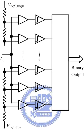
(16) Chapter 2. Chapter 2 Review of High Speed CMOS ADC Architectures. In resent year, there are several architectures to implement high-speed analog-to-digital converters. Each has advantages and disadvantages with a particular combination of speed, accuracy, and power consumption. They all fit into a particular application. These various architectures are based on the search technique used to find appropriate digital representation of the analog input level. The design methodologies for full flash, interpolating, time interleaved, pipelined, and folding architectures will be described in this chapter.. 2.1 Full Flash ADC The full flash architecture is the simplest and fastest analog-to-digital converter. In a full flash analog-to-digital converter, the analog input signal is simultaneously compared to reference values by a bank of comparator circuits. The differences between the input and reference values are amplified to digital levels and generate thermometer code, as shown in Figure 2.1. The thermometer code is easily encoded into binary or gray code. The reference voltages are usually provided by tapping from a resistor reference ladder to generate the monotonic increase of reference voltages from zero to the input full scale. Preamplifiers are often added in front of comparators 4.
(17) Chapter 2 to reduce the overall input-referred offset by lowering the impact of comparator dynamic offset with preamplifier gain.. Vref , high. Vin Binary Output. Vref , low. Figure 2.1 Full flash ADC architecture.. For a N-bit flash ADC, 2 N − 1 comparators and 2 N resistors are needed. Although flash ADC can achieve high speed, but the amount of comparators and resistors depend on the resolution of ADC and this quantity grows exponentially with resolution. Relatively, the resulting circuit is typically very large and consumes a great deal of power. So that, most flash ADC studies have been focused on resolution lower than 8-bit. However, the objective of this work is to design 4GSps 4-bit and 5-bit Nyquist Rate ADC in a 0.18-um CMOS process. Since speed is the top priority, a full flash architecture is a promising candidate to meet the speed target.. 5.
(18) Chapter 2. 2.2 Interpolating ADC The full flash ADC is considered to realize the highest conversion rate but it suffers from not only larger chip size and larger power dissipation, but also lower dynamic performance due to large input capacitance. Consequently, interpolating conception alleviates the effect drastically. The diagram of interpolating architecture is shown in Figure 2.2. Amplitude quantization can be viewed as a collection of zero crossings. The front-end preamplifiers can be followed by differential pairs to perform 2-times interpolation, thereby creating additional zero crossings and increasing the resolution.. Vin Preamplifiers Vy. V R , n +1. Interpolating Amplifiers Vo 2. An +1. Vo3 Binary Output Vx. V R, n. Vo1. An Encoder. Vo3 Vo1 V R, n. Vx Vo 2 V R , n +1. V R, n Vin. V R , n +1 Vy. Figure 2.2 Interpolating ADC architecture.. 6. Vin.
(19) Chapter 2 Interpolation reduces the number of the pre-stages. In other words, interpolation relaxes a number of tradeoffs in the design of the front-end. The preamplifiers typically suffer from the most stringent requirements in terms of input common-mode range, input capacitance, power dissipation, overdrive recovery speed, voltage gain, and capacitive feed-through to the reference ladder. Hence, it is desirable to reduce the number of preamplifiers through the use of interpolation. Another aspect of interpolation is that it does not require precise gain in any of the stages because only the zero crossings carry the information.. 7.
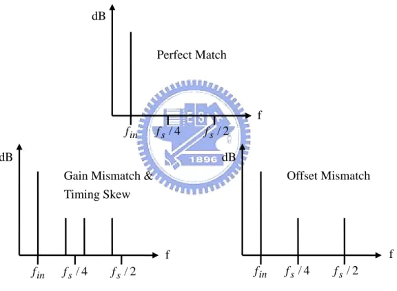
(20) Chapter 2. 2.3 Time Interleaved ADC [8] The time-interleaved technique can be used in nearly any type of ADCs. It consists of M ADCs operating at different clock phases. The corresponding digital multiplexer selects the digital output of each ADC periodically and forms a high speed ADC output as shown in Figure 2.3.. Vin. T/H. K-bit ADC. T/H. K-bit ADC Binary Output K-bit ADC. T/H. Multiplex Ts ADC 1 ADC 2. ADC M t. Figure 2.3 Time interleaved ADC architecture and timing.. Although the clock speed of such a architecture can be very high by just extending the parallel paths, the mismatch issue will then cause the fundamental. 8.
(21) Chapter 2 limitations. Among those are the gain mismatch, the offset mismatch, and the timing mismatch. As shown in Figure 2.4, these problems introduce some distortions, centered around multiples of channel sampling rate as sideband components for channel gain mismatch and timing skew, and at multiples of channel sampling rate as tones for channel offset mismatch. Embedding a track-and-hold circuit in front of each channel can effectively reduce the effects. The clock for the track-and-hold circuit must be operating at the overall ADC speed. When the parallel pipelined architecture has a single track-and-hold circuit, the timing mismatch among the channels is not an issue. Because track-and-hold circuit is distributing sampled signals instead of dynamic signals. dB Perfect Match. f. f in. fs / 4. fs / 2. dB. dB Offset Mismatch. Gain Mismatch & Timing Skew. f. f. f in. fs / 4. f in. fs / 2. fs / 4. fs / 2. Figure 2.4 Spectrum of a reconstructed sinusoid for a four-way converter array.. 9.
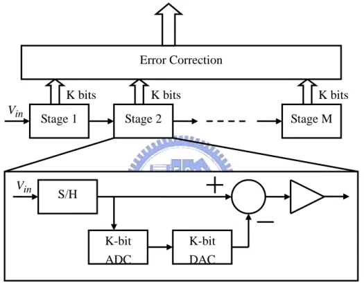
(22) Chapter 2. 2.4. Pipelined ADC The large input capacitive loading of the full ash ADC can be avoided by using. one resolution per stage configuration, leading to the pipelined approach. Basically, the pipelined ADC can inherently have better dynamic performance due to the reduced loading per stage and inter-stage track-and-hold operation. The general block diagram of a pipelined ADC is shown in Figure 2.5.. Error Correction K bits. Vin. Vin. Stage 1. K bits. K bits. Stage 2. Stage M. S/H. K-bit ADC. K-bit DAC. Figure 2.5 Pipelined ADC architecture.. As shown in the figure, the pipelined ADC is basically a residue processing system. The residue contains the required information as well as the imperfections, including offset errors, inter-stage gain errors, inter-stage DAC nonlinearity, and operational amplifier settling-time errors. With digital correction, the effects of offset error, gain error are reduced, while the inter-stage DAC nonlinearity and operational amplifier settling-time errors limit the performance of pipelined ADC. Another drawback is the long latency of pipelined ADC which avoids its application in a closed-loop linear feedback system, however, this is not a problem in wireless communication systems. 10.
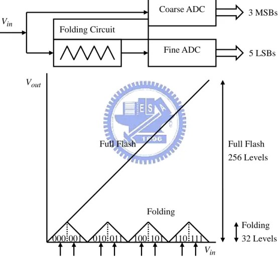
(23) Chapter 2. 2.5 Folding ADC [9] The folding ADC, unlike the pipelined ADC which serially output the digital codes, output them in two parallel paths called coarse and fine quantization, respectively. Therefore, the speed approaching the full flash ADCs is possible with careful design. Typically, it is beyond the pipelined ADC. Figure 2.6 shows the block diagram of a folding ADC of 8-bit resolution associated with its transfer curve.. Vin. Coarse ADC. 3 MSBs. Fine ADC. 5 LSBs. Folding Circuit. Vout. Full Flash. Full Flash 256 Levels. Folding 000 001. 010 011. 100 101. Folding 32 Levels. 110 111. Vin. Figure 2.6 Folding ADC architecture and the transfer curve of a folding circuit in comparison with the full flash ADC.. As shown in the figure, if it is folded 8 times, the MSBs is 3-bit and LSBs 5-bit. If folded 4 times, the MSBs and LSBs are 6-bit and 2-bit respectively, the only 11.
(24) Chapter 2 difference is the encoding method. As a result, the comparator count for the folding converter is 32 for fine and 8 for coarse with a total of 40. It is much less than 255 required by a full flash ADC. Folding architectures exhibit low power and low latency as well as the ability to run at a higher sampling rate. The drawback is the limited dynamic performance due to input frequency multiplication and bandwidth limitation of the folding circuitry.. 12.
(25) Chapter 3. Chapter 3 Design Techniques of Flash ADC. There are several techniques to design a flash ADC. After reviewing many methods which were provided to design a flash ADC in resent years, we propose the most suitable architecture to meet our speed target. In Section 3.1, a detail description about averaging concepts is given. Section 3.2 describes the interpolation concepts. Section 3.3 analyzes several architectures which were provided in resent years. Section 3.4 shows the architectures which are used in our 4-bit ADC and 5-bit ADC circuit design.. 3.1 Averaging Technique In continuous time systems, offsets of amplifiers are the main limitation to increase the converter resolution above 6 bits. However, it has been shown already that sizing the input devices results in a reduction in the offset voltage. This transistor sizing, however, is limited and introduces disadvantages like large input capacitance, large die size and high power dissipation. To partially overcome this problem, an averaging scheme will be introduced. This averaging scheme uses the outputs of more active input pairs to increase the effective gate area and in this way reduce the offset voltages [10].. 13.
(26) Chapter 3. 3.1.1 Resistive Averaging In Figure 3.1 a system using resistive averaging is shown. The figure shows three differential amplifiers with load resistors R1 as part of the input amplifier chain used in a flash analog-to-digital converter. Averaging is obtained by coupling the outputs of the differential amplifiers via averaging resistors R0. This average resistor chain continues to couple more input stages. As long as the input amplifiers are active and operate in the linear signal range, the output signals of these active amplifiers contribute via the averaging resistors to a differential amplifier operating around the “zero crossing” level. The differential pair M3, M4 is the zero crossing one. It is affected by both left and right neighbors.. R1. R1. R1. R1. R0. R1. R1. R0 Vout. R0 M1 Vin. M2. M3. M4. Vrefn-1 Vin. R0. M5. M6. Vrefn Vin. Vrefn+1. Figure 3.1Resistive averaging scheme [11]. As long as the neighboring amplifiers are in the linear region, it looks like that the zero crossing amplifier consists of a much bigger device with a size equal to the sum of the areas of the active linear amplifiers. As a result, a very rough estimation of the reduction in offset voltage compared to a non-coupled single differential amplifier equals to. N active is obtained. Here N active is the number of linear active. amplifier stages contributing to the output signal of the zero crossing stage. Furthermore the signal amplitude increases with a value equal to N active. 14. while the.
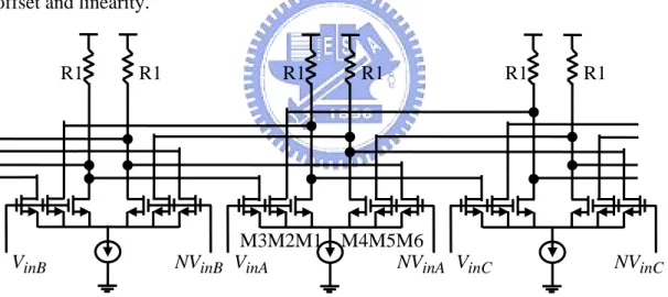
(27) Chapter 3 noise increases with. N active . As a result, the signal-to-noise ratio improves with. N active , and the offset voltage reduces with the same ratio.. 3.1.2 Active Averaging Figure 3.2 shows the circuit diagram of such a system. Again, an averaging construction is shown using three differential pairs. The input pairs in this system are split up into three parts. An equal split is one of the possibilities that can easily be implemented. Starting with the middle pairs consisting of M1 to M6, the output current of M1 and M4 go directly to the load resistors R1 and R2, M2 and M5 to the right, and M3 and M6 to the left. As fro the center stage, the output signal is obtained as the sum of the three neighboring pairs. Therefore, the linearity is improved. Only two extra pairs are required at both ends of the reference ladder. A drawback of this system is that more accurate elements are required to minimize the influence on the offset and linearity.. R1. VinB. R1. R1. R1. M3M2M1 M4M5M6 NVinB VinA NVinA VinC. Figure 3.2 Active averaging scheme. 15. R1. R1. NVinC.
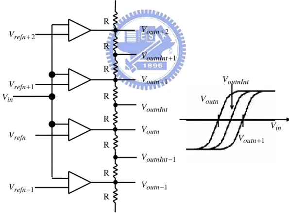
(28) Chapter 3. 3.2 Interpolation The output signals from the input amplifiers have a finite slope. Furthermore the difference between the signals is limited. As a result it is possible to accurately interpolate between two reference levels and obtain an accurate zero crossing of the differential output signal. The number of input amplifiers can be reduced depending on the number of times an interpolation takes place [10].. 3.2.1 Resistive Interpolation In Figure 3.3 shows a resistor interpolation circuit. As shown in this figure, the signal VoutnInt is interpolated between Voutn and Voutn +1 . An extra zero crossing is obtained in this way without an input amplifier.. R Vrefn + 2. Voutn + 2. R. VoutnInt +1 R. Voutn +1. Vrefn +1. Vin. R. VoutnInt. VoutnInt Voutn. R. Voutn. Vrefn. R. VoutnInt −1 R Vrefn −1. Voutn −1 R. Figure 3.3 Resistive interpolation scheme. 16. Vin Voutn +1.
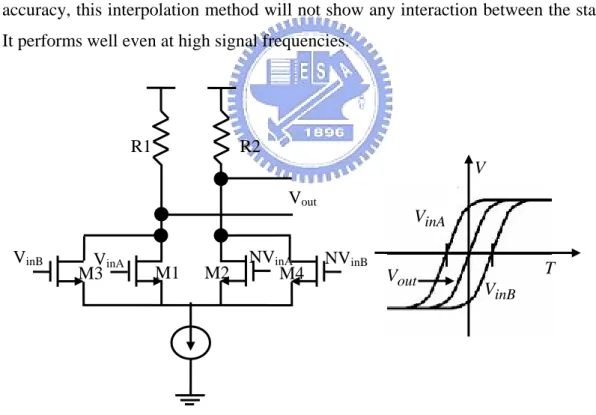
(29) Chapter 3. 3.2.2 Active Interpolation An alternative to resistive interpolation is the active interpolation. In this system amplifier transistors are split up into two equal devices as shown in Figure 3.4. As shown in the figure, all transistors have equal size. A size of 0.5 is given relative to the input differential pairs. At the gates of transistors M1 and M2 the output signal from pairs A is applied, while at the gates of transistors M3 and M4 the output signal of pairs B is introduced. These signals show a delay in time as can be seen from Figure 3.4. The drain currents of M1 and M3 are added as has been done for M2 and M4 too. And these combined drain currents flow through the load resistors R1 and R2. The output signal of this stage interpolates now between the output signal of pairs A and the output signal of pairs B. With witch, the pairs A and B are averaged. As long as offset voltages and mismatches are small as compared to the required interpolation accuracy, this interpolation method will not show any interaction between the stages. It performs well even at high signal frequencies.. R1. R2 V. Vout. VinA VinB. VinA M3. M1. M2. NVinA M4. NVinB. Vout. Figure 3.4 Active interpolation scheme. 17. T VinB.
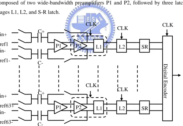
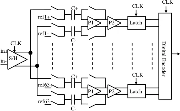
(30) Chapter 3. 3.3 Comparison of Different Design Techniques 3.3.1 6-bit Flash ADC with Auto-zero Technique [12] Figure 3.5 shows an example of a high-speed flash architecture utilizing auto-zero technique. A specific feature of disk-drive read-channel systems is that the conversion cycles are interrupted regularity and an auto-zero function can be performed. During this time, reference levels and comparator offsets are stored on the sampling capacitors C+ and C-. During normal operation the comparators determine the position of the input signal relative to the reference levels. Each comparator is composed of two wide-bandwidth preamplifiers P1 and P2, followed by three latch stages L1, L2, and S-R latch. CLK C+. in+ ref1 in-. P1. ref1-. P2. L1. SR. ref63+ in-. P1. P2. L1. Digital Encoder. C+. ref63-. L2. C-. CLK in+. CLK. CLK. CLK. L2. SR. C-. Figure 3.5 6-bit flash ADC with auto-zero technique. Auto-zero has two drawbacks. It needs series-input capacitors that limit resolution bandwidth, and also requires ”idle time” for offset cancellation. The. 18.
(31) Chapter 3 alternative application of this work is intended for DVD playback that requires no “idle time”.. 3.3.2 6-bit Flash ADC with Sample-and-Hold and Auto-zero Technique [13] The resolution bandwidth and conversation rate degradation due to the series-input capacitors in flash auto-zero architecture can be improved by adding a sample-and-hold circuit. The top level block schematic of this ADC is shown in Figure 3.6. The input is sampled and held by the S/H. An important feature of this architecture is that it uses two interleaved S/H circuits operating at half the sampling frequency. The interleaving has two advantages. First, the acquisition time available for each S/H is twice that which would be available if a single S/H circuit were used. Second, the final output of the S/H is held for an entire clock interval. This dramatically eases the design of the output buffer that drives the comparator array. The output from the S/H is fed into the comparator array which converts the input signal into a digital thermometer code, which is then converted to a 1-of-64 code by the bubble correction logic. This in turn is fed into a ROM type encoder that generates the final 6-bit digital output. The sample-and-hold preceding the series-input capacitors improves the ADC’s resolution bandwidth and sampling rate. However, the improvement will not be as effective as eliminating the input capacitors entirely.. 19.
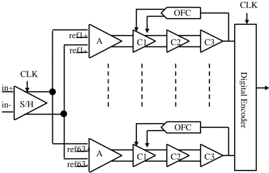
(32) Chapter 3 CLK. CLK. C+ ref1+ P1. P2. Latch. ref1in+ in- S/H CLK. C+. Digital Encoder. C-. CLK. ref63+ P1. P2. Latch. ref63C-. Figure 3.6 6-bit flash ADC with S/H and auto-zero technique. 3.3.3 6-bit Flash ADC with Background Digital Calibration [14] To improve the ADC linearity, series-input capacitors are essential for auto-zero architecture to store and therefore to cancel random offsets of the comparators, which cost speed degradation. Accuracy improvement can also be achieved, without input capacitors, by digital calibration. A block diagram of this ADC is shown in Figure 3.7. The ADC consists of a T/H circuit, 63 preamplifiers, 63 comparators, each having offset calibration circuit, and an interleaved encoder capable of error correction.. 20.
(33) Chapter 3. CLK. OFC ref1+. A. ref1-. C1. C2. C3. Digital Encoder. CLK in+ in- S/H OFC ref63+ A ref63-. C1. C2. C3. Figure 3.7 6-bit flash ADC with background digital calibration. T/H circuits overcome the sampling time skews and the aperture time differences in the comparators to improve the ADC’s conversion rate and resolution bandwidth. The comparator uses three stages to achieve high-speed and low power consumption at the same time. Each offset in the preamplifier and comparator is calibrated by the OFC. The OFC, consisting of an up/down-counter and current sources controlled by the counter outputs, detects the preamplifier and the comparator offsets using the 3rd stage comparator output. These current sources are fed back to the first stage comparator without affecting the comparator speed. Improvement in resolution bandwidth due to T/H circuit is clearly shown on measurements. The background digital calibration allows smaller transistors in analog signal path to achieve high conversion rate without accuracy degradation but costs half of the active die area. Bandwidth limitations on preamplifier and comparator stages seem to limit the maximum achievable speed of this architecture.. 21.
(34) Chapter 3. 3.3.4 6-bit Flash ADC with Distributed T/Hs and Resistive Interpolation [15][16] The analog preprocessing circuitry is shown in Figure 3.8. The analog preprocessing circuit converts the differential input signal into 65 parallel signals which are connected to the comparator inputs. The gain in this analog preprocessing block is realized by a cascade of amplifier stages. A sampling operation is inserted after the first stage. The analog bandwidth of the first amplifiers up to the sampling switches determines the analog signal bandwidth of the converter, while the bandwidth of the amplifiers after the sampling switch relates to the sampling rate and the required settling time. Only the first stage operates in continuous-time mode, demanding linear behavior over the complete input signal bandwidth in the cascade of subsequent amplifier stages. CLK. refRef+. A1. B1. C1. D65 Digital Encoder. in-. C35. Averaging network & Termination. in+. B19. Averaging network & Termination. A1. Distributed Track-and-Hold. ref-. Averaging network & Termination. ref+. CLK. D1. Figure 3.8 6-bit flash ADC with distributed T/H and resistive interpolation. The first set of amplifiers A1 through A11 are connected to a reference resistor ladder and to the differential signal input. The first and last amplifiers in combination with the reduced resistors R1-R2 implement the termination circuit. The averaging resistors also implement a first interpolation: the averaging resistors are divided in 22.
(35) Chapter 3 two parts, each with a value of R2/2. After sampling, the signals are amplified (B1…B19) and interpolated again, generating 34 parallel differential outputs. These outputs act as inputs for the third amplification (C1…C34) and interpolating stage. The combination of the fourth amplifier stage and the comparator stage generates 65 parallel digital output signals which are clocked through 65 flip-flops. Even though the distributed T/H circuits improve the conversion rate by pipelining the analog path, they suffer dynamic inaccuracies due to skews in the clock signals distributed across the array like any parallel scheme. A single front-end T/H with sufficient linearity outperforms the distributed T/H at high input frequencies. The cascaded amplifier stage with averaging, which is necessary to alleviate the comparator offset, degrades the conversion rate and resolution bandwidth due to its limited overall signal bandwidth.. 3.3.5 6-bit Flash ADC with Resistive Averaging [17] Figure 3.9 shows a flash ADC with balanced circuits in the T/H, reference ladder, and other preamplifiers for second-order distortion cancellation. The T/H is designed for 8-bit linearity with the highest possible bandwidth. The preamplifier array with a gain of 3 senses the difference between the differential input signal and the differential threshold to drive the latched comparator. However, the preamplifiers in the array suffer from random offsets. Collective averaging of the preamplifier outputs across a properly designed resistor network lowers the impact of the offsets, improving accuracy of the threshold comparison without degrading bandwidth. A comparator must quickly recover from large overdrive when the changing input voltage rapidly approaches the comparator’s threshold from far away. To aid this, the gain of the comparator’s input differential pair is about one, which widens its bandwidth. The resulting net amplification of 3 is not sufficient to overcome the dynamic random offsets in the regenerative latch for 6-bit accuracy. Resistor averaging is also used within the comparators to lower the impact of offsets. Interpolation is not used in this work, because it degrades bandwidth. The second comparator array provides rail-to-rail logic swing for the digital back end consisting of the S-R latch and ROM-based digital encoder.. 23.
(36) Chapter 3 CLK CLK ref1+ ref1-. A2. A1. in- T/H. ref63+ ref63-. A1. A2. L1. L2. Digital Encoder. in+. L2. Averaging network. Averaging network. CLK. L1. CLK. Figure 3.9 6-bit flash ADC with resistive averaging. Even though the two stages of resistive averaging reduces the random offsets without degrading bandwidth. It needs add lots of dummy amplifiers on the top and bottom of each averaging resistor network to compensate the band linearity errors. It trades power consumption and chip area for wider linear input range.. 24.
(37) Chapter 3. 3.4 Design Issues and Architecture of Ultra High Speed Flash ADC After analyzing the various type of high speed flash ADC, a suitable architecture and design issues for high speed operation is detailed.. 3.4.1 Design Guidelines After studied varies design, we have come up with the following design guide lines. 1. Auto-zero should be avoided since the series-input capacitors degrade the speed. 2. Track-and-Hold should be included to improve resolution bandwidth. 3. Replacing distributed T/H with single front-end T/H avoids clock skew. 4. Background digital calibration should be avoided since it is area-inefficient and needs complicate control timing. 5. Offset averaging should be included for accuracy improvement. 6. Replacing resistive averaging with active one saves power consumption and avoids dummy amplifiers. 7. Trade-off between one or two stages averaging meets the requirement of accuracy. 8. Interpolation could be included for power consumption and chip area reduction. 9. Replacing resistive interpolation with active one achieves high speed operation. 10. Cascaded continuous time amplifiers should be avoided to improve the overall signal bandwidth before latch. 11. Reset switches should be added in comparator for fast overdrive recovery [18]. 12. Reset switches should be avoided in preamplifier behind reference ladder for low kick back noise. 13. Speed and gain of comparator are optimized by cascading preamplifier and latches [19]. 14. Replacing ROM-based digital encoder with logic one achieves high speed operation [16].. 25.
(38) Chapter 3. 3.4.2 4-bit 4-GSps Flash Architecture The flash architecture shown in Figure 3.10 includes a front-end T/H, a reference ladder, 15 comparators for quantization, and a thermometer-Gray-binary digital encoder. The comparator has three stages to improve speed, a continuous time preamplifier, the first latch with reset switch, and the second latch with reset switch. The resolution of this ADC is only 4-bit. It does not need offsets averaging techniques due to its low accuracy. The detail circuit implementation will be discussed in Chapter 4.. ref+. A15. CLK. CLK. 1st Latch. 2nd Latch. CLK. ref-. in+ in- T/H CLK ref-. A1. 1st Latch. CLK 2nd Latch. ref+. Figure 3.10 4-bit flash ADC architecture. 26. Digital Encoder. CLK. 4 bit.
(39) Chapter 3. 3.4.3 5-bit 4-GSps Flash Architecture Using Active Averaging Technique The flash architecture shown in Figure 3.11 includes a front-end T/H, a reference ladder, 31 comparators for quantization, two dummy amplifiers for preamplifiers, and a thermometer-Gray-binary digital encoder. The comparator of quantization also has three stages to improve speed, a continuous time amplifier and latch with reset switch, first latch with reset switch, and second latch with reset switch. The resolution of this ADC is 5-bit, and it needs offset averaging techniques for higher accuracy. An active averaging is used in this ADC. The detail circuit implementation will be discussed in Chapter 4 and Chapter5.. 27.
(40) Chapter 3 CLK ref1+. A32. ref1CLK. CLK. CLK A31. in+ in- T/H. PA31. Latch CLK. CLK 1st Latch. 2nd Latch CLK 2nd Latch. PA30. CLK A2 PA2. A1. Latch CLK Latch. CLK 1st Latch CLK 1st Latch. CLK 2nd Latch CLK 2nd Latch. PA1 ref1-. A0. ref1+. Figure 3.11 5-bit flash ADC with active averaging technique. 28. Thermometer to Gray to Binary Digital Encoder. Latch. 1st Latch. 5 bit.
(41) Chapter 3. 3.4.4 5-bit 4-GSps Flash Architecture Using Active Interpolation Technique The flash architecture shown in Figure 3.12 includes the same sub circuits described in previous section. To save power consumption and chip area, an active interpolation is used in this ADC. This technique reduces the number of amplifiers of preamplifier stages from 33 to 16. The detail circuit implementation will be discussed in Chapter 4 and Chapter5.. 29.
(42) Chapter 3. CLK ref1+. A15. Latch. CLK 1st Latch. CLK. CLK. 2nd Latch. ref1PA31. CLK. CLK. CLK. CLK Latch. in+ in- T/H. PA30. Latch. CLK 1st Latch. 2nd Latch CLK 2nd Latch. PA29. CLK A1 PA3. Latch CLK Latch. PA2. CLK. CLK 1st Latch CLK 1st Latch CLK. CLK 2nd Latch CLK 2nd Latch CLK. ref1ref1+. A0. Latch. 1st Latch. 2nd Latch. PA1. Figure 3.12 5-bit flash ADC with active interpolation technique. 30. Thermometer to Gray to Binary Digital Encoder. A14. CLK. 1st Latch. 5 bit.
(43) Chapter 4. Chapter 4 A 4-bit 4 GSps Flash ADC Circuit Design. Based on the design methodologies and circuit architecture at the end of chapter 3, the circuit implementation and related issues will be discussed in detail in this Chapter. The required resolution is 4-bit, targeting to sampling rate above 3.125GSps and maximally at 4GSps. In Section 4.1, the design issues target on the ultra high speed front-end T/H. Section 4.2 shows how the preamp recovers from large overdrive. Section 4.3 describes the operation of the first latch. Section 4.4 gives the advantage of clocked S-R latch. Section 4.5 explains how to use combinational logic to create digital encoder. Section 4.6 considers the high speed full swing clock input and digital code output. Section 4.7, the whole chip design considerations are given. Finally, summary the circuits in 4-bit architecture.. 4.1 Front-End Track-and-Hold The front-end track-and-hold circuit improves the dynamic performance of an ADC. Due to the usage of the front-end track-and-hold circuit, the distributed time skew problem of quantization is alleviated. For gigahertz sampling rate operation, T/H becomes essential to achieve the desired converter resolution with wide input bandwidth. Thus, the performance requirements of an ADC, especially dynamic 31.
(44) Chapter 4 linearity, shift to the T/H circuit design. The open loop T/H architecture shown in Figure 4.1 is the most popular for high sampling rate. The T/H consists mainly of a sampling switch, a holding capacitor, and unity gain buffers on the input and output. This simple architecture makes it. possible to design for very high speed. Since it does not have the benefits of feedback, the accuracy cannot be high.. Input Buffer. Output Buffer SW. Vin. Vout CH. Figure 4.1 Track-and-Hold in open loop configuration. Differential structure has several benefits over single ended structure. The circuit is less sensitive to common mode noise. The clock-feed-through error is ideally zero. Finally, the even order distortion tones are significantly reduced. However, the source follower is the best choice for unity gain buffer in the open loop structure. Unfortunately, it is difficult to design a fully differential source follower. Thus, [20] has proposed the pseudo-differential T/H as shown in Figure 4.2. SW. CH. Vin. Input Buffer. Output Buffer. Vout. CH. SW. Figure 4.2 Pseudo-differential type Track-and-Hold in open loop configuration 32.
(45) Chapter 4. The T/H circuit shown in Figure 4.3 precedes the flash quantization [17]. The circuit is constructed as follows: First, the dummy switches are used to absorb signal-dependent charge injection and clock feed-through released from the sampling switches [21][22]. Second, the holding capacitors are made large enough to overcome the gate capacitance variation of the MOSFET. Third, the buffer is made by PMOS whose bulk is connected to its source to suppress the body effect.. clk. clkb. CH. Vout Vin clk. clkb. CH. Figure 4.3 Track-and-Hold with PMOS constant current source. In Figure 4.3, the constant current source follower is the simplest realization of a unity gain buffer. But, it still has limitation and drawback. When the input to the buffer is fast and has large amplitude, the slew rate at the output of the circuit is limited. Thus, its speed can not be linearly improved by increasing the bias current. Although we can suppress the body effect by connecting its bulk to source, its gain still can not reach real unity. Due to the finite output resistance, its gain can only approximate 0.9~0.92. So, another source follower buffer had been provided [23], as shown in Figure 4.4. This push-pull structure has very good slewing properties. Its gain can be larger than unity due to cascade gain. Well controlling the cascade 33.
(46) Chapter 4 transistor to obtain the unity gain. However, it still has the drawback that the large input swing forces the cascade transistor entering triode region easily. This causes the buffer distortion. Furthermore, the non-linearity of the source follower makes T/H poor in dynamic performance.. Vin. Vout. Figure 4.4 PMOS push-pull source follower buffer. As discussed above, we use the buffer structure that combines the constant current source follower and push-pull source follower. In NMOS example, Figure 4.5 shows three types of pseudo-differential buffers. Figure 4.5(a) has the best linearity but the worst slewing property and less than unity gain. Figure 4.5(b) is a push-pull source follower. It has the best slewing property but the worst linearity. Its gain is controlled for unity. Figure 4.5(c) is a new NMOS source follower. Well control the ratio of two source followers can obtain the wanted slewing property. The gain of this buffer approximates unity. We also obtain the enough linearity for our T/H spec.. 34.
(47) Chapter 4. VINB. VIN. VOUTB. VOUT. Vbn (a). VINB. VIN. VOUTB. VOUT. (b). VINB. VIN. VOUTB. VOUT. (c). Figure 4.5 (a) NMOS constant current source follower, (b) NMOS push-pull source follower (c) NMOS constant current & push-pull source follower. Based on the new source follower, Figure 4.6 shows the T/H architecture. The input buffer is contributed with NMOS whose bulk is connected to its source to suppress the body effect by using deep N-well process, and the output buffer with PMOS.. 35.
(48) Chapter 4. Input Buffer. CLK. Output Buffer. Vin. Vout. Figure 4.6 New pseudo-differential architecture. Full view of the T/H circuit schematic diagram is shown in Figure 4.7. The sampling switches charge injection and clock feed-through cause distortion by adding or removing charge on the holding capacitor when they disconnects the signal source. Dummy switches driven by the complement of the switch clock mainly lower the common mode jump. Because both drain and source of the dummy switches are connected to the holding capacitor, their size ratios are initially chosen as half the size of switches. Then, they are fine tuned through simulation. For ultra high speed operation, the input common mode voltage must be high, 1.3V, and the output common mode voltage of the input buffer for sampling must be low. Then the common mode voltage of sampling signal passing through the output buffer becomes high again. Due to the low sampling common mode voltage, 0.5V, only NMOS for the sampling and dummy switches are used in order to obtain the high speed.. 36.
(49) Chapter 4. Vin. CLK. CLK. CLKB. CLKB. Figure 4.7 Track-and-Hold circuit schematic diagram. Vout. 37.
(50) Chapter 4. 4.2 Preamplifier The main purpose of the preamplifier is to provide information about the difference between input signal and reference voltage generated by a resistor reference ladder. For high speed operation, the preamplifier stage should be wideband with sufficient gain to overcome the comparator offsets. It should also recover from large overdrive within one clock cycle. Figure 4.8 shows the simplest differential amplifier. It is a open-loop single-pole and has large gain-bandwidth. Although adding a reset switch can improve the operation speed, it induces kick-back noise to the reference ladder. Thus we choose the continuous-time amplifier without a reset switch for preamplifier [17].. VOUT. VOUTB. VINB. VIN. Figure 4.8 Open-loop single-pole amplifier. The following analysis addresses the fundamental limitation of an open-loop single-pole amplifier in the overdrive recovery. The preamplifier is completely unbalanced at t=0-. With a step input applied to the preamplifier at t=0+, the output transient is shown in Figure 4.9. The step response of the amplifier is given by. (. ). Vout (t ) = ( A ⋅ ∆V + I ⋅ R ) ⋅ 1 − e − t / τ − I ⋅ R. (4.1). where A is the voltage gain, ∆V is the voltage difference between the input and reference tap, I is the tail current, and τ is the time constant.. 38.
(51) Chapter 4. G ⋅ ∆V. 0. A ⋅ ∆V. I ⋅ R drop. Vout. Period (T) Time. Figure 4.9 Step-input response of preamplifier. The overdrive recovery time is calculated by setting Vout (t ) of Eq. (4.1) to zero.. (. ). −t /τ Vout t re cov ery = 0 = ( A ⋅ ∆V + I ⋅ R ) ⋅ ⎛⎜1 − e re cov ery ⎞⎟ − I ⋅ R ⎝ ⎠. (4.2). Solving Eq. (4.2) for t re cov ery gives t re cov ery = −. I ⋅R ⎞ ⎛ ⋅ ln⎜1 − ⎟ A ⋅ ∆V + I ⋅ R ⎠ 2πf − 3db ⎝ 1. (4.3). Assume that the output step response does not settle within one clock cycle as shown in Figure 4.9. The gain-bandwidth requirement to obtain the desired gain ( G = Vout (t = T ) / ∆V ) can be derived from Eq. (4.1). The output voltage at t=T is given by. (. ). Vout (t = T ) = G ⋅ ∆V = ( A ⋅ ∆V + I ⋅ R ) ⋅ 1 − e − T / τ − I ⋅ R. (4.4). Solving Eq. (4.4) for f − 3db gives. f − 3db = −. 1 ⎛ ( A − G ) ⋅ ∆V ⎞ ⋅ ln⎜ ⎟ 2πT ⎝ A ⋅ ∆V + I ⋅ R ⎠. ⎧ 1 ⎛ ( A − G ) ⋅ ∆V ⎞⎫ GBW = A ⋅ f − 3db = A ⋅ ⎨− ⋅ ln⎜ ⎟⎬ ⎝ A ⋅ ∆V + I ⋅ R ⎠⎭ ⎩ 2πT. (4.5). (4.6). Given period (T), desire gain (G), and LSB ( ∆V ), R = A / g m and g m ∝ I , variables A and I decide the gain-bandwidth (GBW). Assume that DC gain (A) is 39.
(52) Chapter 4. about 3. The GBW required to obtain gain more than unity (G > 1) to overcome the offset of the first latch in one period (T=250ps) of 4 GHz sampling rate is 6.36 GHz. The higher the DC gain, the lower the required GBW. However, increasing the load resistor for higher gain also lowers the output common mode. That will cause the input transistors enter the triode region and lower the operation speed of the first latch. Based on the simple open-loop single-pole amplifier, Figure 4.10 shows our fully differential preamplifier. The input signal and reference voltage are all differential.. 1.4k. 1.4k Vo1. Vo2. Vref1. Vin1. Vin2. Vref2. Vbn 0.5mA. 0.5mA. Figure 4.10 Fully differential open-loop single-pole preamplifier. 40.
(53) Chapter 4. 4.3 First Latch The latch shown in Figure 4.11 operates at 1.35GHz clock rate in 0.35-um CMOS process [17]. The output of the preamplifier drives the first latch. The first latch stage provides large enough output swing to second latch in the worst case. As the preamplifier, overdrive recovery limits highest ADC clock frequency. Due to the continuous time preamplifier separating kick back noise, it is possible to insert reset switch between the two output nodes to optimize power at highest clock frequency.. CLK M3. M4. Msw. Vo1. Vo2 CLK Vin1. M7 M5 M1. Vbn. M8. CLK. M2 M6. Vin2. M9 0.7mA. Figure 4.11 First latch circuit. While the track-and-hold is in track mode, the reset switches are turned on to erase the residual voltage from the previous overdriving. During this reset mode, it output is reset through two parallel discharge paths for fast overdrive recovery. When the track-and-hold is in hold mode, the reset switches are turned off. During this regeneration mode, differential pair (M1, M2, and M9) configured from cross-couple inverters (M1-M4) steer the tail current from one side to the other, speeding up regeneration. Figure 4.12 shows the operation of the first latch.. 41.
(54) Chapter 4. (a) Reset mode. CLK. vdd. gnd. CLK. CLK. Vin1. Vin2. (b) Regeneration mode. off − ∆V. ∆V. off. off. Figure 4.12 Two first latch operation mode, (a) reset mode, (b) regeneration mode. 42.
(55) Chapter 4. 4.4 Second Latch Although the first latch provides large enough output swing, it is still not reaching the rail-to-rail logical level. Thus, adding another latch to provide rail-to-rail swing is needed. But, this has some drawback. First, it consumes more power and area when adding second latch array. Second, the second latch may not reach rail-to-rail level at high clock rate. So, combining the clocked latch and continuous time S-R latch can easily reach rail-to-rail logic level and obtain fast overdrive recovery [12][17]. Based on the first latch architecture, the second latch is designed without the tail current to save power at regeneration mode. Changing the back to back inverters with two cross-coupled PMOS lowers the parasitic capacitance to improve the regeneration speed. Figure 4.13 shows the second latch. When the second latch output in single-end, it must add a dummy inverter at the non-used node to balance the regenerative speed.. M6. M5. Vo1. Vo2 CLK. M3. M4. CLK. Vin1. M1. M2. Vin2. Figure 4.13 Second latch circuit. 43.
(56) Chapter 4. 4.5 Digital Encoder In many converters, different internal coding schemes are used before the final binary code is generated. Function of the digital encoding for flash ADC is to convert the thermometer code into binary code. Many digital encoding schemes have been developed to suppress glitch errors caused by the meta-stability of the comparators [24][25] and bubbles in the thermometer code [26][27]. Meta-stability errors occur when non-binary comparator levels drive the digital encoder and produce senseless outputs. The meta-stable state can be suppressed by increasing the clock period and/or the gain during the regeneration phase. In our work, cascading two latch stages lowers the meta-stable error at the same clock period. There are three major sources that induce bubble errors. The first source is that overall input-referred random offset being greater than 0.5 LSB can switch the order of the two adjacent thresholds. The second source is that zero-crossings occur in different time delay due to the comparators have no front-end track-and-hold. The third source is the different propagation delay through each comparator path. In our work, the analysis of the random offset decides whether to average or not. Adding the front-end track-and-hold circuit eliminates the clock skew dependent bubble errors. Inserting reset switches to first latch and second latch suppresses the propagation delay dependent bubble errors. Except the analog methods described above, using Gray encoding can also suppress the mete-stability and bubble error. The probability of mete-stable states can be lowered because in Gray encoding no signal is applied to more than one input. That allows the use of pipelining to increase the time for regeneration. The effect of bubbles is reduced because the accuracy of the Gray code degrades gradually as more bubbles appear in the thermometer code. Table 4-1 shows the correspondence among thermometer, Gray, and binary codes of 4-bit.. 44.
(57) Chapter 4. Binary Code. Gray Code. Thermometer Code. 0000. 0000. 000000000000000. 0001. 0001. 000000000000001. 0010. 0011. 000000000000011. 0011. 0010. 000000000000111. 0100. 0110. 000000000001111. 0101. 0111. 000000000011111. 0110. 0101. 000000000111111. 0111. 0100. 000000001111111. 1000. 1100. 000000011111111. 1001. 1101. 000000111111111. 1010. 1111. 000001111111111. 1011. 1110. 000011111111111. 1100. 1010. 000111111111111. 1101. 1011. 001111111111111. 1110. 1001. 011111111111111. 1111. 1000. 111111111111111. Table 4-1 Binary-Gray-thermometer code implementation. At ultra high speed operation, logic based encoder is more suitable than ROM based encoder [25]. Logic based encoder can be pipelined easily for higher speed operation. Each thermometer bit influences only one Gray bit (as shown in the 4-bit example in Figure 4.14) [28]. Extra delay cells are added to match the delay difference among the signal paths. The Gray code is converted to binary code using two-input EXOR cells with delay matching. To operate at 4GHz sampling rate and beyond, the D-flip-flops are implemented with true single-phase clocked (TSPC) circuits [29].. 45.
(58) Chapter 4. Bin3. Gray3. Th8. DQ. Th4 Th12b Th2 Th6b. Bin2. Gray2 DQ. Bin1. Gray1 DQ. Th10 Th14b Th1 Th3b Th5 Th7b. Bin0. Gray0 DQ. Th9 Th11b Th13 Th15b. CLK. Figure 4.14 Digital encoder. Although this encoder is very fast, it is still not fast enough to operate at 4GHz. The propagation delay of the critical path is longer than one period (250ps). Thus, pipelining the circuit is needed. The modified digital encoder is shown in Figure 4.15. Extra delay cells (shaded lines) are added to match the delay mismatch.. 46.
(59) Chapter 4 Th8 Th4 Th12b Th2 Th6b Th10 Th14b Th1 Th3b Th5 Th7b Th9 Th11b Th13 Th15b. Delay Cell. Gray3 Gray2. Gray1. CLK. Delay Cell. Gray0. Delay Cell. Figure 4.15 Pipelined digital encoder. Bin3. Bin2. Bin1. Bin0. 47.
(60) Chapter 4. 4.6 Clock Generator and Output Driver In this ADC, clock jitter randomly modulates the periodic sampling instants of the T/H. Non-uniform sampling raises the noise floor of the digitized system and degrades the signal-to-noise ratio (SNR). Clock jitter is major a concern for high-speed ADCs. Given a sinusoidal input waveform with amplitude A and radian frequency ω , the SNR due to clock jitter only is. ⎛ ⎞ A2 / 2 ⎟ = −20 ⋅ log(ω ⋅ δT ) SNR = 10 ⋅ log⎜ ⎜ A2 ⋅ ω 2 ⋅ δ 2 / 2 ⎟ ⎝ ⎠. (4.7). where δT is the rms clock jitter [30]. According to Eq. 4.7, to obtain SNR of 26 dB (the ideal SNR for 4-bit quantization of a sine wave) at input frequency of 2GHz, the rms clock jitter should be less than 4 ps. Low-noise methods taken from analog circuit design are applied to the clock generator (see Figure 4.16). The circuits convert a differential sine wave with 600mV amplitude input into two phases full swing clock. Then, it is followed by stages of ratio inverters to drive the clock load for this ADC.. Vin1. CLK. Vin2. Vin1 CLKB. Vbn. Figure 4.16 Clock generator. In order to drive the output load at ultra high speed operation, the driving circuit 48.
(61) Chapter 4. is composed of open-drain configuration, Figure 4.17. Each single-ended mode with output swing of 200mV needs 18mA driving current.. 50Ω. Off-Chip. 2nH. 1pF. Binary code. Figure 4.17 Open-drain output driver. 49. 0.8pF.
(62) Chapter 4. 4.7 Whole Chip Design Issues The chip floorplan is shown in Figure 4.18. Noise. Small. Large. Analog Decoupling Capacitance. Reference Ladder. Track-and-Hold. Digital Decoupling Capacitance Comparator Array. Bias. Clock Generator. Digital Encoder. Large. Sensitivity of noise. Output Driver. Small. Figure 4.18 Layout floorplan. In order to avoid large supply and ground bounce, decoupling capacitors are added in analog and digital blocks. The power supply basically divides the chip layout into three domains. The large distance between analog and digital circuits couple less noise from digital to analog. The sensitive analog lines should be as short as possible. The guard ring and device matching techniques are implemented as well. The chip layout is shown in Figure 4.19.. 50.
(63) Chapter 4. Figure 4.19 Layout of the 4-bit 4GSps flash ADC. 51.
(64) Chapter 4. 4.8 Summary The key features of this work are now summarized. A front-end T/H for these flash ADCs enables beyond Nyquist input up to 4GHz conversion rate. Continuous time preamplifier provides low kick back noise. Reset switches in the first latch and the second latch give fast overdrive recovery. The second latch is the fastest such CMOS circuit with rail-to-rail output. Replacing the ROM-based encoder with logic-based encoder and using pipeline technique in the encoder improves the operation speed. Using thermometer-Gray-binary digital encoder lowers the bubble errors.. 52.
(65) Chapter 5. Chapter 5 A 5-bit 4 GSps Flash ADC Circuit Design. Based on the 4-bit 4GSps architecture and circuit described in Chapter 4, two 5-bit architectures and related issues will be discussed in detail in this Chapter.. The. required resolution is 4-bit, and the sampling rate above 3.125GSps and maximally at 4GSps. In section 5.1, the design issues on the higher gain preamplifier for the comparators are presented. Section 5.2 introduces how to use active averaging to improve accuracy and Section 5.3 introduces how to use active interpolation to add one more bit. Section 5.4 compares the difference of circuit between the 4-bit and 5-bit architecture.. 5.1 Preamplifier The preamplifiers described in previous chapter use passive load. Although using passive load has larger GBW than using active load, it is hard to increase gain without changing tail current and bandwidth. Thus, active load preamplifiers are usually used in folding or flash architectures. Figure 5.1(a) shows the PMOS diode-connected load differential amplifier, and the small-signal differential gain can be derived using the half-circuit concept.. 53.
(66) Chapter 5. (. ). g −1 // rON // rOP ≈ − mN Av = − g mN ⋅ g mP g mP. (5.1). where subscripts N and P denote NMOS and PMOS respectively. Expressing g mN and g mP in terms of device dimensions, we have Av ≈ −. µ n (W / L ) N | (VGS − VTH )P | = (VGS − VTH )N µ p (W / L )P. (5.2). The PMOS diode-connected load consumes voltage headroom, thus creating a trade-off between the output voltage swings, the voltage gain, and the input common mode range. From Eq. 5.2, for given bias current and input device sizes, gain and PMOS overdrive voltage scaled together. To achieve a higher gain, (W / L )P must be decreased, thereby increasing | (VGS − VTH )P | and lowering the common mode. level. In order to alleviate the above difficulties, part of the bias currents of the input transistors can be provided by PMOS current sources. Illustrated in Figure 5.1(b), the idea is to lower the g mP by reducing their current rather than their aspect ratio [31].. VBP. VO1. VO2. VO1. VO2. VIN2. VIN2 VIN1. VIN1. VBN. VBN. (a). (b). Figure 5.1 (a) Differential pair with diode-connected PMOS and (b) adding current sources to increase the voltage gain. 54.
數據
+7
相關文件
General overview 1-2–1-3 Reference information 6-1–6-15 Emergency Power Off button 6-11 Focusing the video image 4-3 Foot Switches 6-14. General Overview 1-2
如圖,已知平行四邊形 EFGH 是平行四邊形 ABCD 的縮放圖形,則:... 阿美的房間長 3.2 公尺,寬
This project aims to cover a range of learning targets and objectives in the Knowledge, Interpersonal and Experience Strands/Dimensions, language development strategies and
To prepare students to face their future challenges in the 21 st century, the General Studies curriculum bears the notions of developing students’ understanding about themselves,
Arts education is one of the five essential learning experiences in the overall aim of education set out by the Education Commission: “To enable every person to attain all-
Ex.3 the threshold value U t ( 150 mJ) required to ignite airborne grains... 5-3 Capacitors
年青的學生如能把體育活動融入日常生活,便可提高自己的體育活動能
常識科的長遠目標是幫助學生成為終身學習者,勇於面對未來的新挑 戰。學校和教師將會繼續推展上述短期與中期發展階段的工作
