國 立 交 通 大 學
電子工程學系 電子研究所碩士班
碩 士 論 文
藉由大氣電漿沉積主動層之氧化鋅
薄膜電晶體之研究
Investigation on Thin-Film-Transistors with Zinc-Oxide Active
Layer Deposited by Atmosphere –Pressure Plasma Jet
研 究 生:吉家威
指導教授:張國明 博士
中華民國 中華民國中華民國
藉由大氣電漿沉積主動層之氧化鋅
薄膜電晶體之研究
Investigation on Thin-Film-Transistors with Zinc-Oxide Active
Layer Deposited by Atmosphere –Pressure Plasma Jet
研 究 生:吉家威 Student:Chia-Wei Chi
指導教授:張國明 博士 Advisor:Dr. Kow-Ming Chang
國 立 交 通 大 學
電子工程學系 電子研究所碩士班
碩 士 論 文
A Thesis
Submitted to Department of Electronics Engineering and Institute of Electronics College of Electrical and Computer Engineering
National Chiao Tung University in Partial Fulfillment of the Requirements
for the Degree of Master in Electronics Engineering
August 2010
Hsinchu, Taiwan
中華民國 中華民國中華民國 中華民國 九十九十九十九十九九九九 年年年 八年 八八八 月月月 月藉由大氣電漿沉積主動層之氧化鋅
薄膜電晶體之研究
學生:吉家威 指導教授:張國明 博士
國立交通大學電子工程學系
電子研究所碩士班
摘要
本論文利用大氣電漿沉積氧化鋅作為元件的主動層,並且成功發展 出高效能的薄膜電晶體。在X光繞射儀(XRD)分析中可以發現由大氣電 漿沉積之氧化鋅具有優選的(002)晶向。氧化鋅薄膜對可見光的穿透率超 過80%,並且具有3.25eV的能隙。這些特性使得大氣電漿沉積氧化鋅具 有應用於透明電路的潛力,以及能減少光漏電對於元件的影響。我們首 先利用矽晶片作為元件的基板並且逐一量測與比較各種實驗參數對元 件的影響,在主動層厚度、基板加熱溫度、以及製程氣體等實驗參數中 取得最佳化,並且發展出具有開關電流比2.3×10⁷ 、電遷移率3.21cm2 /Vs、臨界電壓27.3V、次臨界擺幅 3.83 V/decade的高性能薄膜電晶體。 我們在論文中使用X光繞射儀 (XRD)、掃描式電子顯微鏡(SEM)、光激 螢光光譜(PL)來分析及討論不同製程參數的氧化鋅薄膜中的結晶品質、 缺陷種類及密度、表面形貌等等,以及利用元件的I-V轉換曲線來進行 元件特性的探討。最後我們將最佳製程參數的電晶體製作在玻璃基板 上,以證明本論文所採用之方法與理論是可以應用在量產的AMOLED 及AMLCD電路設計中,並且使用不同的閘極絕緣層材料使臨界電壓從 27.3V降低至11.8V。Investigation on Thin-Film-Transistors with
Zinc-Oxide Active Layer Deposited by
Atmosphere –Pressure Plasma Jet
Student:Chia-Wei Chi Advisor:Dr. Kow-Ming Chang
Department of Electronics Engineering and Institute of Electronics
National Chiao Tung University, Hsinchu, Taiwan
Abstract
In this thesis, we have successfully developed a high performance thin film transistor (TFT) with zinc oxide active layer deposited by atmosphere pressure plasma (APP) jet. Zinc oxide films show strongly preferred (002) orientation in XRD analysis. Zinc oxide films have over 80% transmittance of visible light and band gap energy 3.25eV. Therefore zinc oxide films deposited by APP jet are suitable for transparent devices. Wide band gap can release the issue of photo-excited leakage current. At first, we fabricated TFTs on silicon substrate. Experimental parameters of APP jet which we tested and compared including thickness of active layer, hot plate temperature, carrier gas, and main gas. We have developed high performance devices with an on/off ratio of 2.3×10⁷ ,a saturation mobility of 3.21cm2 /Vs, a threshold voltage of 27.3V, a gate voltage swing of 3.83 V/decade. In this thesis, several material analysis techniques, such as XRD, SEM, and PL were utilized to discussing the crystallization, grain size, and
surface morphology of ZnO films. Electrical characteristics and conduction mechanisms of ZnO TFTs were also investigated by I-V characteristic analysis. We have fabricated TFTs successfully with ideal experimental parameters on glass substrate. It can prove that our experiments are feasible for real and mass manufacturing in AMOLED or AMLCD. The threshold voltage becomes lower from 27.3V to 11.8V because the hydrogen in gate insulator SiN:H would diffuse to active layer as donors.
致謝
本論文承蒙 張國明老師悉心指導才能完成,僅此表達最深的謝 意,老師在碩士生涯兩年中不斷給予我人生方向的指引及學業的諄諄教 誨,讓我在作研究或是待人接物上都受益良多。 感謝實驗室中指導我研究的 菘宏學長,他總是身先士卒地帶領著 我們進行各項實驗以及研究,講解實驗過程的機制,與我們討論各項分 析儀器的操作細節與原理,增加我們專業領域的知識並且解答心中的種 種疑惑。最重要的是給予我們一個可以學習的研究者典範,並展現實事 求是的精神,在此表示最由衷的感謝。 感謝 士軒學長在實驗思考的指導與協助,總能使我受益匪淺。感 謝跟我同組的同學 偉強以及 煒力長久以來在工研院作實驗的陪伴與 合作,以及感謝工研院的工程師 哲蔚和 文宗對我實驗上的幫助。並且 我要感謝ED632實驗室裡的每一位成員,你們總是帶來歡樂的氣氛,並 且適時的給予我研究上的幫助。 最後,我要感謝二十五年來一直養育我支持我的家人,以及跟我交 往六年對我不離不棄的女友均維。你們是我最堅強的精神支柱,讓我即 使歷經失敗也不曾有過放棄的念頭。這篇論文不是我一個人的力量可以 完成的,謹將這份成果獻給所有幫助過關懷過我的人。Contents
摘要 摘要摘要 摘要··· i Abstract··· ii 致謝 致謝致謝 致謝··· iv Chapter 1 Introduction ··· 1 1.1 Forward ···1 1.2 Motivation···2Chapter 2 Literature Reviews··· 5
2.1Reviews of thin film transistors applications ···5
2.2Reviews of ZnO TFTs···9
Chapter 3 Experiments ··· 23
3.1 Experimental Procedures···23
3.2 TFTs fabricated on glass substrate ···28
3.3 Material analysis equipments ···30
Chapter 4 Results and Discussions ··· 39
4.1 Parameters of depositing ZnO films···39
4.2 Thickness of ZnO in TFTs ···40
4.3 Hot plate temperature···45
4.4 Carrier gas···47
4.5 Main gas···49
4.6 TFTs on glass substrate···51
Chapter 5 Conclusions ··· 68
Chapter 6 Future Works ··· 69
Table Captions
Table 2-1Table of electrical properties and conditions……….22
Table 3-1 APP jet experimental parameters………..38 Table 4-1 Electrical properties of devices with different active layer
thickness………65 Table 4-2 Electrical properties of devices with different hot plate
temperature………...…65 Table 4-3 Electrical properties of devices with different carrier gas………66 Table 4-4 Electrical properties of devices with different O2 ratios in main
gas………..66 Table 4-5 Electrical properties of devices on different substrates…………66 Table 4-6 Table of ZnO TFTs electrical properties and process conditions of
Figure Captions
Figure 2-1 (a) Top Gate Structure (b) Bottom Gate Structure……..……….17
Figure 2-2 (a)PMOLED(b) PMOLED Control Circuit………...17
Figure 2-3(a)AMOLED (b)AMOLED Control Circuit………...18
Figure 2-4 ALD four steps………...…….…18
Figure 2-5 ZnO TFT fabricated by ALD………..…………....19
Figure 2-6 Magnetron sputtering………..………....19
Figure 2-7 ZnO TFT fabricated by RF magnetron sputtering…………...…20
Figure 2-8 Pulsed laser deposition………...……….20
Figure 2-9 Sol-gel process……..……….… .21
Figure 2-10 ZnO deposited by Sol-gel process with thermal treatments…..21
Figure 3-1 Schematic illustration of experimental procedures……….23
Figure 3-2 APP jet diagram………...33
Figure 3-3 Scanning path………...………...………33
Figure 3-4 Patterns on mask………...………...34
Figure 3-6 Lift-off procedures ………..………35
Figure 3-7 ZnO TFTs structure on silicon substrate……...………...36
Figure 3-8 ZnO TFTs structure on glass substrate...……….36
Figure 3-9 Patterns on mask for devices on glass substrate…………...…...37
Figure 3-10 ZnO TFTs on glass substrate………...…………...37
Figure 3-11 Photoluminescence………...……….38
Figure 4-1 SEM images of real zinc oxide thickness…………...………….52
Figure 4-2 XRD analysis of different thickness films………...………53
Figure 4-3 Transmittance of different thickness zinc oxide on glass substrate……….53
Figure 4-4 PL(Photoluminescence) analysis of 50nm zinc oxide……...…..54
Figure 4-5 TFTs ID-VG curve with VD=80V…………...………..54
Figure 4-6 Drain current and gate current with active layer=30nm………..55
Figure 4-7 TFTs ID-VD curve with active layer=50nm…………...………55
Figure 4-8 XRD analysis of 10nm zinc oxide………..…………56
Figure 4-10 Top view SEM images with different temperature……...……57
Figure 4-11 ID-VD curve of devices with different hot plate temperature....58
Figure 4-12 ID-VG curve with CDA and N2 as carrier gas………..…..59
Figure 4-13 ID-VG curve with different ratios oxygen in main gas……..…59
Figure 4-14 The relationship between O2 ratio and mobility……..……….60
Figure 4-15 The relationship between O2 ratio and threshold voltage..…...60
Figure 4-16 Trap states in band gap………...………...61
Figure 4-17 PL spectrum of different oxygen ratios………...………..61
Figure 4-18 XRD (101)(002)(100) diffraction peaks………...………62
Figure 4-19 SEM images of different O2 ratios………...……….63
Figure 4-20 ID-VG curve and IG-VG curve of TFTs on glass substrate……..64
Figure 4-21 ID-VD curve of TFTs on glass substrate……….64
Chapter 1
Introduction
1.1 Forward
Display technologies are very important industries in Taiwan, and create the value of output near one trillion new Taiwan dollars every year. Many products we use day-to-day like PC screens, note book computers, and cell phones contain display technologies. TFT-LCD has been developed for a long time in display technologies. Amorphous silicon (a-Si:H) thin film transistors (TFTs), which are used widely as drivers of TFT-LCD module like Active Matrix Liquid-Crystal Display (AMLCD), which integrates TFT-LCD and backlight source module. For thinner screens and wider angle of view, Active Matrix Organic Light Emitting Diode (AMOLED) has been the leading role of display technologies recently.
But the deadly issue of the material based on a-Si:H in active layer in TFTs is low field effect mobility (~0.5cm2˙V-1˙S-1)[1], photo sensitivity (low band gap about 1.7eV) and rather high deposition temperature (~400℃ ) [2],[3]. Since the band gap of a-Si is in visible regime, the photo excited carriers (photo current effect) might make the array of AMLCD and AMOLED out of control. For this reason, the opaque metals to keep a-Si based channel blind from visible light are integrated necessarily. This causes lower opening of AMLCD pixels and more complicated device fabrication.
important development and target of display technologies. Display technology based on OLED is demonstrated to promising for providing lightweight, power efficient, and high brightness performance at reasonable voltage and current levels. And AMOLED does not need backlight source module because OLED can produce light by itself. But the issue we need to solve is that driving OLEDs need higher voltage and driving current than LCDs for controlling circuit. However, the driving circuit seems difficult for us to use the a-Si based material for the low mobility limited.
So the material based on zinc oxide as active layer in TFTs becomes the better choice than a-Si because ZnO TFTs have a advantageous property about high field effect mobility [4]. Zinc oxide is the ideal material for active layer in TFTs which can achieve the purpose of efficient power consumption, low fabrication temperature, and good driving ability [5].
1.2 Motivation
In fact, we can deposit thin film composed with zinc oxide by several ways, including chemical methods and physical methods and. Different thin film fabrication mechanisms would influence the characteristics of zinc oxide like grains size, defect kinds, and thin film quality very much. Another aspect we need to consider is prime cost during all the device manufacturing process. And the process integration of ZnO TFTs must be suitable for several different substrate materials like silicon wafer for research and glass for real mass manufacturing.
ZnO thin film deposited for TFTs reveals polycrystalline with a hexagonal wurtize structure and has a preferred orientation with the c-axis
perpendicular to the substrate [6]. Intrinsic ZnO film behaves as an n-type transparent semiconductor due to the defects such as oxygen vacancies. In fact, oxygen vacancies in zinc oxide could supply free electrons. It has a wide band gap (~-3.37eV) with optical transmission over 80% in the visible portion of the electromagnetic spectrum. Besides that, thin films based on ZnO have been studied for several years for their low cost, low photo sensitivity, and high field effect mobility.
Recently, many teams announced their reports abort fabrication methods to ZnO TFTs, including RF magnetron sputtering[7], atomic layer deposition (ALD)[8], and pulsed laser deposition (LPS)[9]. But physical deposition and ALD need to be operated in vacuum chamber because reducing the probability that radicals and ions meet collision with vapor molecules during deposition. In this way, RF or DC magnetron sputtering and atomic layer deposition are not feasible for real and mass manufacturing because of high prime cost and low throughput, even ZnO TFTs by using them to fabricate have better electrical properties than normal chemical depositions.
Some chemical solution depositions do not need be operated in vacuum chamber, but there are many impurities and defects which we could not forecast in ZnO thin film. So the quality of ZnO become worse and is not ideal for TFTs. Besides that, chemical solution depositions usually need high fabrication temperature (>400℃ to provide enough energy for ) molecules debonding and chemical reaction. It is difficult to integrate high temperature process in TFTs fabrication if the substrates are glass and flexible material. Synthesizing all above-mentioned fabrication methods
issues, we studied the device properties of TFTs with ZnO film as active layer deposited by atmospheric pressure plasma jet.
We paid much attention to atmospheric pressure jet because this kind of plasma does not require a complicated vacuum system which would reduce the cost of processing and enlarge the size limit [10]. Moreover, atmospheric pressure plasma jet is also a low temperature process. The temperature of plasma could be as low as 200℃ which could reduce the thermal damage of substrate and even be applied for plastic substrate. APP jet is suitable for large area substrate because of no vacuum chamber in APP jet systems. And the most important reason of using APPCVD is the quality of ZnO film deposited by this fabrication method is well enough to be the channel layer of TFTs .
In this paper, studies will be undertaken to interpret the growth mechanism of ZnO films, crystallographic structure, and electrical properties of the films and TFTs. We have explored experimentally as functions of the deposition conditions and defined an optimal deposition condition for TFT including fabrication temperature, thickness of film, main gas and carrier gas during deposition process. And we integrated ZnO TFT with an optimal deposition condition on glass substrate to proof that it is feasible to make a transparent device by our fabrication method. By considering the electrical properties , the mechanisms of film growth, and the influences of different conditions will be reported and discussed later.
Chapter 2
Literature Reviews
2.1Reviews of thin film transistors applications 2.1.1Thin film transistors
A thin-film transistor (TFT) is a special kind of field-effect transistor made by depositing thin films of a semiconductor active layer as well as the dielectric layer and metallic contacts over a supporting substrate[11]. A common substrate is glass, since the primary application of TFTs is in liquid crystal displays. This differs from the conventional transistor where the semiconductor material typically is the substrate, such as a silicon wafer.
TFTs can be made using a wide variety of semiconductor materials. A common material is silicon. The characteristics of a silicon based TFT depend on the crystalline state. That is, the semiconductor layer can be either amorphous silicon, microcrystalline silicon, or it can be annealed into polysilicon. Other materials which have been used as semiconductors in TFTs include compound semiconductors such as cadmium selenide and metal oxides such as Zinc Oxide. TFT's have also been made using organic materials (referred to as an Organic TFT or OTFT).
By using transparent semiconductors and transparent electrodes, such as indium tin oxide (ITO), some TFT devices can be made completely transparent[12]. Because the substrate cannot withstand the high annealing temperature, the deposition process has to be completed under relatively low
temperature. Chemical vapor deposition, physical vapor deposition are applied.
There are two main TFTs structures which are shown in figure2-1. The structure A is top gate structure and structure B is bottom gate structure. We choose one of two structures in TFTs fabrication by practical requirements and issues. The structure of top gate conforms our original ideals naturally because this structure has been used in normal field effect transistors for many years. But majority of TFTs fabrications does not adopt this structure .
We need to consider that process of dielectric layer deposited by PECVD or other deposition ways would maybe influence semiconductor active layer by plasma bombarding or thermal treatment. Defects and interface charges would appear in active layer and the interface between dielectric layer and active layer. In this way, electrical properties of top gate structure TFTs become worse by defects and interface charges.
We usually adopt bottom gate structure in advanced TFTs fabrication for better quality of semiconductor active layer than top gate structure because the active layer is deposited after gate dielectric layer and drain or source electrode. Using this structure avoids plasma bombarding or thermal treatment injuring active layer . And another benefit of bottom gate structure is that we can fabricate devices on silicon substrates as gate electrodes. So the gate leakage would deal little influence to devices because we use thermal oxide to be gate insulator. In this way, we can focus on the active layer of TFTs. But a new problem we need to solve about bottom gate structure is the stability of devices after active layer exposed to the air
directly after a long time. Mists and particles would invade active layer and made the reliability of devices become worse.
In this way, an effective method to solve this problem is depositing preservation layer on active layer like silicon nitride to avoid mists and particles invading active layer. This method would increase the prime cost and influence the active layer, but we choose bottom gate structure to avoid plasma bombarding or thermal treatment injuring active layer .
2.1.2 TFTs as OLED drivers
Passive matrix organic light emitting diode (PMOLED) is a display technology as shown in figure 2-2(a) [13, 14]. OLED describes a specific type of thin display technology which doesn't require a backlight.An OLED is driven by one data line and one scan line at one time order. At one time order only one scan line would be the grounding and other scan lines connect to broken circuit. The next time order the below scan line would be the grounding .This action is ordered from first scan line to last scan line and repeat again and again. When one scan line became grounding, OLEDs which be connected to it would be driven by data lines as shown in figure 2-2(b) [15].
Persistence of vision is the main mechanism of PMOLED to form images to our eyes because OLEDs keep radiating only during one time order. When monitors size became larger, for keeping ideal persistence of vision ,we need to drive OLEDs by large current and high voltage to make them radiating more light. But this movement would make OLEDs having short lifetime and large power consumption. So it is necessary to find out a method to keep OLEDs radiating before scan line connected to grounding
and accepting data line the next time.
Active-matrix OLED (Active-matrix organic light-emitting diode) is a display technology for use in mobile devices and televisions. And Active-Matrix refers to the technology behind the addressing of pixels. AMOLED technology continues to make progress towards low-power, low-cost, and large size (e.g. 40-inch) for applications such as TV.
An active-matrix OLED (AMOLED) display consists of OLED pixels that have been deposited or integrated onto a thin film transistor (TFT) array to form a matrix of pixels that generate light upon electrical activation as shown in figure 2-3(a), which functions as a series of switches to control the current flowing to each of the pixels as shown in figure 2-3(b).
Typically, this continuous current flow is controlled by at least two TFTs at each pixel ,one to start and stop the charging of a storage capacitor and the second to provide a voltage source at the level needed to create a constant current to the pixel and eliminating need for the very high currents required for passive OLED matrix operation.
Active-matrix OLED displays provide higher refresh rate than their passive-matrix OLED counterparts, and they consume significantly less power. This advantage makes active-matrix OLEDs well suited for portable electronics, where power consumption is critical to battery life. The amount of power the display consumes varies significantly depending on the color and brightness shown.
2.2Reviews of ZnO TFTs
ZnO thin film deposited for TFTs reveals polycrystalline with a hexagonal wurtize structure and has a preferred orientation (002) with the c-axis perpendicular to the substrate. Zinc oxide has several advantages[16, 17]:
1. Cost down and abundant 2. Wide band gap~3.3eV 3. High mobility
4. Bipolarity material (n-type or p-type with different dopants)
And using zinc oxide to replace a-Si as active layer in TFTs has many Advantages[18, 19]:
1. High filed-effect mobility (> 1cm2˙V-1˙S-1)
2. Low deposition temperature
3. Wide band gap (~3.3eV) 4. Stability
2.2.1 ZnO TFTs Fabricated by Atomic Layer Deposition
Atomic layer deposition (ALD) is a thin film deposition technique that is based on the sequential use of a gas phase chemical process. The majority of ALD reactions use two chemicals, typically called precursors. These
precursors react with a surface one-at-a-time in a sequential manner. By exposing the precursors to the growth surface repeatedly, a thin film is deposited.
ALD is a self-limiting (the amount of film material deposited in each reaction cycle is constant), sequential surface chemistry that deposits conformal thin-films of materials onto substrates of varying compositions. ALD is similar in chemistry to chemical vapor deposition (CVD), except that the ALD reaction breaks the CVD reaction into two half-reactions, keeping the precursor materials separate during the reaction. Due to the characteristics of self-limiting and surface reactions, ALD film growth makes atomic scale deposition control possible. By keeping the precursors separate throughout the coating process, atomic layer control of film growth can be obtained as fine as ~0.1 Å (10 pm) per monolayer. Separation of the precursors is accomplished by pulsing a purge gas (typically nitrogen or argon) after each precursor pulse to remove excess precursor from the process chamber and prevent 'parasitic' CVD deposition on the substrate.
The growth of material layers by ALD consists of repeating the following characteristic four steps as shown in figure 2-4:
(1) Exposure of the first precursor.
(2) Purge or evacuation of the reaction chamber to remove the non-reacted precursors and the gaseous reaction by-products.
(3) Exposure of the second precursor or another treatment to activate the surface again for the reaction of the first precursor.
(4) Purge or evacuation of the reaction chamber.
Transparent ZnO thin film transistor was fabricated on glass substrate. The field effect mobility is about 1~10 cm2/Vs. The active layer (ZnO), gate insulator (Al2O3 or SiN), and source–drain electrode (ZnO:Al) were
deposited by atomic layer deposition as shown in figure 2-5. The carrier density of the ZnO layer was carefully adjusted to reduce off-current of TFT. Good contact with small contact resistance was formed between the active layer and the source–drain electrode. The on-off ratio of ZnO TFTs fabricated by ALD is about 106~108.
The four main factors contributing to obtain well-behaved ZnO-TFTs by ALD method were the reduction of the carrier amount of ZnO film by lowering the growth temperature, minimal damage to the surface of dielectric during the S/D and active layer processes, the high quality of the dielectric layer grown by ALD, and the good ohmic contact between the S/D and the active layer resulting in ZnO TFT performance suitable for an OLED driving device. Although the wet etching of the active layer degraded the TFT performance, it showed promise as a large area transparent display. The active layer process temperature was as low as 100°C and was also compatible with a plastic substrate to realize a flexible display.
The major limitation of ZnO TFTs fabricated by ALD is its slowness and high prime cost; usually only a fraction of a monolayer is deposited in one cycle. Fortunately, the films needed for future-generation ICs are very thin and thus the slowness of ALD is not such an important issue. Although the selection of film materials grown by ALD is wide, many technologically
important materials cannot currently be deposited by ALD in a cost-effective way. ALD is a chemical technique and thus there is always a risk of residues being left from the precursors.
2.2.2 ZnO TFTs Fabricated by RF Magnetron Sputtering
Sputter deposition is a physical vapor deposition process for depositing thin films, sputtering means ejecting material from a target and depositing it on a substrate such as a silicon wafer. The target is the source material. Substrates are placed in a vacuum chamber and are pumped down to a prescribed process pressure. Sputtering starts when a negative charge is applied to the target material causing a plasma or glow discharge. Positive charged gas ions generated in the plasma region are attracted to the negatively biased target plate at a very high speed. This collision creates a momentum transfer and ejects atomic size particles form the target. These particles are deposited as a thin film into the surface of the substrates.
Magnetron sputtering can be done either in DC or RF modes. DC sputtering is done with conducting materials. If the target is a non conducting material the positive charge will build up on the material and it will stop sputtering. RF sputtering can be done both conducting and non conducting materials. Here, magnets are used to increase the percentage of electrons that take part in ionization of events and thereby increase the probability of electrons striking the Argon atoms as shown in figure 2-6, increase the length of the electron path, and hence increase the ionization efficiency significantly.
magnetron sputtering on Si substrates held near room temperature. The best devices had field-effect mobility of more than 2 cm2/Vs and an on/off ratio about 105~107. With high optical transparency ~80% for wavelength 400nm.The combination of transparency in the visible, excellent transistor characteristics, and low-temperature processing makes ZnO thin-film transistors attractive for flexible electronics on temperature sensitive substrates.
2.2.3 ZnO TFTs Fabricated by Pulsed laser deposition
Pulsed laser deposition (PLD) is a thin film deposition (specifically a physical vapor deposition, PVD) technique where a high power pulsed laser beam is focused inside a vacuum chamber to strike a target of the material that is to be deposited as shown in figure 2-8. This material is vaporized from the target (in a plasma plume) which deposits it as a thin film on a substrate (such as a silicon wafer facing the target). This process can occur in ultra high vacuum or in the presence of a background gas, such as oxygen which is commonly used when depositing oxides to fully oxygenate the deposited films.
While the basic-setup is simple relative to many other deposition techniques, the physical phenomena of laser-target interaction and film growth are quite complex (see Process below). When the laser pulse is absorbed by the target, energy is first converted to electronic excitation and then into thermal, chemical and mechanical energy resulting in evaporation, ablation, plasma formation and even exfoliation. The ejected species expand into the surrounding vacuum in the form of a plume containing many energetic species including atoms, molecules, electrons, ions, clusters,
particulates and molten globules, before depositing on the typically hot substrate.
Bottom-gate-type thin film transistors using ZnO as an active channel layer have been constructed. The ZnO layers were deposited using pulsed laser deposition at 400 °C, and the material that was formed had a background carrier concentration of less than 5×1016 cm-3. A double layer
gate insulator consisting of SiO2 and SiNx was effective in suppressing
leakage current and enabling the ZnO TFT to operate successfully. The Ion /Ioff ratio of ZnO TFTs fabricated on Si wafers was more than 105 and the optical transmittance of ZnO TFTs fabricated on glass was more than 80%. These results show that it is possible to fabricate a transparent TFT that can even be operated in the presence of visible light. But the deposition temperature of PLD is too high. It makes ZnO thin-film transistors fabricated by pulsed laser deposition not attractive for flexible electronics on temperature sensitive substrates.
2.2.4 ZnO TFTs Fabricated by Sol-Gel Process
The sol-gel process, known as a chemical solution deposition in atmospheric pressure[20], is a wet-chemical technique widely used in the fields of materials science and ceramic engineering. Such methods are used primarily for the fabrication of materials (typically a metal oxide) starting from a chemical solution which acts as the precursor for an integrated network of either discrete particles or network polymers. Typical precursors
are metal alkoxides and metal chlorides, which undergo various forms of hydrolysis and polycondensation reactions.
In this chemical procedure, the 'sol' (or solution) gradually evolves towards the formation of a gel-like diphasic system containing both a liquid phase and solid phase whose morphologies range from discrete particles to continuous polymer networks. In the case of the colloid, the volume fraction of particles (or particle density) may be so low that a significant amount of fluid may need to be removed initially for the gel-like properties to be recognized. This can be accomplished in any number of ways. The simplest method is to allow time for sedimentation to occur, and then pour off the remaining liquid. Centrifugation can also be used to accelerate the process of phase separation.
Removal of the remaining liquid (solvent) phase requires a drying process, which is typically accompanied by a significant amount of shrinkage and densification. The rate at which the solvent can be removed is ultimately determined by the distribution of porosity in the gel. The ultimate microstructure of the final component will clearly be strongly influenced by changes imposed upon the structural template during this phase of processing.
Afterwards, a thermal treatment, or firing process, is often necessary in order to favor further poly-condensation and enhance mechanical properties and structural stability via final sintering, densification and grain growth. One of the distinct advantages of using this methodology as opposed to the
more traditional processing techniques is that densification is often achieved at a much lower temperature. Sol-gel process was shown in figure 2-9.
The precursor sol can be either deposited on a substrate to form a film, cast into a suitable container with the desired shape, or used to synthesize powders. The sol-gel approach is a cheap and low-temperature technique that allows for the fine control of the product’s chemical composition. Even small quantities of dopants, such as organic dyes and rare earth elements, can be introduced in the sol and end up uniformly dispersed in the final product. It can be used in ceramics processing and manufacturing as an investment casting material, or as a means of producing very thin films of metal oxides for various purposes.
ZnO films deposited by sol-gel process for TFTs need a thermal treatment over 500℃ to make the grains size becoming larger as shown in figure 2-10. It makes ZnO thin-film transistors fabricated by sol-gel not attractive for flexible electronics on temperature sensitive substrates. The TFTs fabricated by sol-gel have a field effect mobility about 0.5~1 cm2/V s and an on-off ratio 104 ~106 in previous literatures. We find some devices fabricated by different methods data which is listed in table 2-1.
Figure 2-1 (a) Top Gate Structure (b) Bottom Gate Structure
(a) (b)
(a) (b)
Figure 2-3(a)AMOLED (b)AMOLED Control Circuit
Figure 2-5 ZnO TFT fabricated by ALD
Figure 2-7 ZnO TFT fabricated by RF magnetron sputtering
Figure 2-9 Sol-gel process
(a) 600℃ treatment (b) 700℃ treatment
(c) 800℃ treatment (d) 900℃ treatment
Table 2-1 Table of electrical properties and conditions On-off ratio Mobility (cm2˙V-1˙S-1) Temperature (℃℃℃℃) Condition ALD 105~107 2~15 <100℃℃℃℃ Vacuum RF Sputtering 104~107 1~10 <50℃℃℃℃ Vacuum Pulsed Laser 104~106 1~5 400 ℃℃℃℃ Vacuum Sol-gel 103~105 <1 500 ℃℃℃℃ Atmosphere Pressure
Chapter 3
Experiments
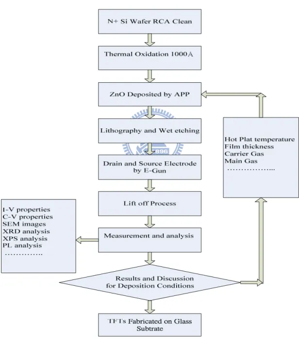
3.1 Experimental Procedures
The experimental procedures listed below:
3.1.1 ZnO deposited by APP jet on Si wafer
In our Literature Reviews, the fabrication and properties of bottom gate type thin film transistors using an intrinsic ZnO film as active layers will be described. We chose bottom gate structure to be the fabrication of TFTs on n+type silicon wafer as substrate. We usually adopt bottom gate structure in advanced TFTs fabrication for better quality of semiconductor active layer than top gate structure because the active layer is deposited after gate dielectric layer and drain or source electrode. Using this structure avoids plasma bombarding or thermal treatment injuring active layer .Silicon wafer was TFTs gate electrode, and we chose n+type silicon wafer for lower gate electrode resistance and bias voltage in gate electrode than n-type Si wafer.
After RCA clean procedure, silicon wafer was put in furnace for oxidation process. Silicon dioxide was chosen as the gate insulator. And the thickness of gate insulator was 1000Å. Temperature of thermal oxidation was 1000℃ with 90minutes. We chose this slightly thick thickness because we did not want the gate leakage current to influence device I-V properties. And then ZnO thin film was deposited by APP jet as active layer with the deposition conditions including hot plate temperature, ZnO thickness, different kinds of main gas and carrier gas, different ratios of oxygen in main gas.
We needed to find out the suitable deposition conditions for promoting the quality of zinc oxide deposited by APP jet. To fabricate ZnO TFTs with good electric properties and high transparence was our goal. So the
procedure of ZnO deposited by APP jet was the most important step in TFT fabrication.
The zinc oxide thin films were deposited by APP jet as shown in figure 3-2 (the sketch of diagram isn’t proportioned to the real size of equipment). N+ silicon wafers were placed on hot plate with suitable process temperature. Zn(NO3)2 water solution was used as the precursors to deposit
ZnO thin film. The concentration of Zn(NO3)2 water solution was 0.2M .
We chose a suitable gap distance as 5mm to deposit ZnO thin film with good quality. The carrier gas carried mists of Zn(NO3)2 water solution to the
plasma region. The carrier gas and mists of Zn(NO3)2 water solution were
mixed with main gas, and these gases would become plasma by arcing mechanism because of high pulsed voltage. Zn(NO3)2 , H2O, carrier gas, and
main gas would participate with some reactions in plasma region. And then main gas would carry these plasmas to substrate and reduce the plasmas temperature. We could use a computer to control scanning path including starting point and terminal point. The scanning path was shown in figure 3-3. The main gas carried plasmas to substrate and the zinc oxide films were deposited by chemical vapor deposition.
Chemical vapor deposition (CVD) is the process of depositing a solid film on the wafer surface through one or more volatile precursors, which react or decompose on the substrate surface to produce the desired deposit. Frequently, volatile by-products are also produced, which are removed by gas flow through the reaction chamber. The sample surface or its vicinity is heated in order to provide additional energy to the system to drive the
reactions. The plasma and radicals would cause reactions and nucleation on samples, and then zinc oxide films would grow from island shape to continuous films.
The experimental parameters of APP jet are shown in table 3-1. The thickness of active layer(scan times), hot plate temperature, carrier gas, and main gas are experimental parameter which we would change in order to discuss the influences to devices and to find out the best parameters for electrical properties. We would use these parameters to fabricate devices on glass substrate. Other experimental parameters are suitable for high quality films so we would not change them during each experiment like gap distance, gas flow rate, and nozzle speed.
3.1.2 Patterning
After ZnO deposited, the next step was to define each TFT’s active layer region. This procedure was carried out in lithography area by photo resist spinner and mask aligner. The patterns on mask for defining active layer region, drain electrodes, and source electrodes is shown in figure 3-4. We etched zinc oxide layer by 0.5% hydrochloric acid water solution with 15 seconds after photo resist had been put cover over zinc oxide as a barrier layer for the region which we wanted to reserve.
When zinc oxide which we did not want to reserve had been etched completely, the next step was to define drain and source electrodes . At the first we though the procedures of defining drain and source electrodes were depositing aluminum and etching it by lithography and wet etching. But the active layer was under drain and source electrodes. It is very difficult to
choose suitable acid solution which kept good etching selectivity between aluminum and zinc oxide. Zinc oxide would be etched very quickly by all acid solution which would etch aluminum. So we used a special technique to replace etching process to define drain and source electrodes on active layer. This special technique was lift-off. The procedures of TFTs fabricated on n+ silicon before lift-off process as shown in figure 3-5. These procedures contained thermal oxidation, ZnO thin films deposited by APP jet, and defining active layer region by lithography technique.
3.1.3 Lift-off
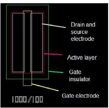
Lift-off process contains several steps as shown in figure 3-6. First we put photo resist as a cover over zinc oxide region which we did not want aluminum deposited. And then we used E-Gun to deposit aluminum about 1000Å on Si wafer. At last, we put Si wafer in acetone with ultrasonic shaking to lift off all photo resist and aluminum on it. So a part of aluminum would stay on active layer as drain and source electrodes. And the device as shown in figure 3-7 would be measured electrical properties and the results would be discussed in next chapter.
3.2 TFTs fabricated on glass substrate
After we found out the best parameters to fabricate zinc oxide active layer in TFTs on silicon substrate, we tried to fabricate devices on Asahi display glass substrate AN100. If the devices on glass substrate could work and still has high performances, we could prove that our experiments are feasible for real and mass manufacturing. The ZnO TFT structure is shown in figure 3-8.And the patterns on mask are shown in figure 3-9. The ZnO TFTs on glass substrate are shown in figure 3-10.
At first TaN 50nm was deposited by sputter on glass substrate as gate electrode, and then we defined the gate electrode region by first mask. We reduced the area of gate electrode to reduce RC time delays.
The reason of using TaN to replace Al is that TaN has better thermal stability. It was very important because the next PECVD process would be proceeded in high temperature(400 ℃ ) conditions. And then we used PECVD to deposit SiN:H (210nm) as the gate insulator. The thickness of SiN:H was chosen because the capacitance of gate insulator would be same to the capacitance of thermal oxide. The reason of using SiN:H to replace SiO2 being gate insulator is the thickness of SiN:H thicker than SiO2 with
the same capacitance because of SiN:H has larger dielectric constant than SiO2.
In this way, the gate leakage current would reduce because of thicker gate insulator. Another reason is there is many hydrogen in SiN:H because the raw materials of depositing SiN:H in PECVD are SiH4 and NH3. The
hydrogen in SiN:H would defuse to zinc oxide as donors. Donors near the interface of gate insulator and active layer could reduce the threshold voltage of device[21]. And then we defined gate insulator region by second mask. The active layer, drain electrode, and source electrode were defined by the same methods of TFTs on silicon substrate. We used the third mask to define active layer region and the forth mask to define drain and source electrodes region including lift-off process.
3.3 Material analysis equipments
3.3.1 SEM
The scanning electron microscope (SEM) is a type of electron microscope that images the sample surface by scanning it with a high-energy beam of electrons in a raster scan pattern[22]. The electrons interact with the atoms that make up the sample producing signals that contain information about the sample's surface topography, composition and other properties such as electrical conductivity.
The types of signals produced by an SEM include secondary electrons, back-scattered electrons (BSE), characteristic X-rays, light, specimen current and transmitted electrons. Secondary electron detectors are common in all SEMs, but it is rare that a single machine would have detectors for all possible signals. The signals result from interactions of the electron beam with atoms at or near the surface of the sample. In the most common or standard detection mode, secondary electron imaging or SEI, the SEM can produce very high-resolution images of a sample surface, revealing details about less than 1 to 5 nm in size. Due to the very narrow electron beam, SEM micrographs have a large depth of field yielding a characteristic three-dimensional appearance useful for understanding the surface structure of a sample.
We used SEM to observe the thickness of ZnO films and surface configuration. Top views of SEM images could take the information about grains size or roughness to us.
3.3.2X-ray Diffraction
In an X-ray diffraction measurement, a crystal is mounted on a goniometer and gradually rotated while being bombarded with X-rays, producing a diffraction pattern of regularly spaced spots known as reflection. The two-dimensional images taken at different rotations are converted into a three-dimensional model of the density of electrons within the crystal using the mathematical method of Fourier transforms, combined with chemical data known for the sample. Poor resolution (fuzziness) or even errors may result if the crystals are too small, or not uniform enough in their internal makeup .X-ray crystallography is related to several other methods for determining atomic structures. Similar diffraction patterns can be produced by scattering electrons or neutrons, which are likewise interpreted as a Fourier transform. If single crystals of sufficient size cannot be obtained, various other X-ray methods can be applied to obtain less detailed information; such methods include fiber diffraction, powder diffraction and small-angle X-ray scattering. In all these methods, the scattering is elastic; the scattered X-rays have the same wavelength as the incoming X-ray. By contrast, X-ray scattering methods are useful in studying excitations of the sample, rather than the distribution of its atoms.
We used XRD to observe ZnO film and obtain information about crystalline structure and grain size. Polycrystalline ZnO has a (002) peak in typical x-ray diffractogram. And using Scherrer formulation
D = Kλ/βcosθ to calculate grain size. D is grain size. K is instrument parameter. λ is the wavelength of X-ray.
3.3.3 Photoluminescence analysis
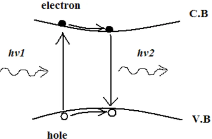
Photoluminescence (abbreviated as PL) is a process in which a substance absorbs photons (electromagnetic radiation) and then re-radiates photons. Quantum mechanically, this can be described as an excitation to a higher energy state and then a return to a lower energy state accompanied by the emission of a photon. This is one of many forms of luminescence (light emission) and is distinguished by photoexcitation (excitation by photons), hence the prefix photo. The period between absorption and emission is typically extremely short, in the order of 10 nanoseconds. Under special circumstances, however, this period can be extended into minutes or hours.
PL analysis is shown in figure 3-10, we use He-Cr laser (325nm) to be the incident ray hv1 to the material surface. The laser would arouse electrons jumping to conduction band from valence band. There would appear electron-hole pairs. After a short time, the electrons recombined with holes in valence band. And hv2 as emergent ray would radiate out from material surface. We can detect hv2 to know the material band gap energy. If there are many trap states in band gap, the intensity of hv2 will reduce because electrons are trapped in trap states.
Figure 3-2 APP jet diagram
Figure 3-4 Patterns on mask
(a)N+ Silicon wafer after RCA Clean (b)Thermal Oxidation
(c)ZnO Thin Film deposited by APP jet (d) Defining active layer region
(a) ZnO deposited on SiO2 (b)Photo resist on Si wafer
(c) Defined electrodes region (d)Al deposited by E-Gun
(e)Lift off P.R. and Al on it (f)Electrodes stayed on active layer
Figure 3-7 ZnO TFTs structure on silicon substrate
Figure 3-8 ZnO TFTs structure on glass substrate
Glass Substrate SiN:H VGS TaN ZnO Al Al VDS N+ Si Wafer Substrate Thermal Oxide ZnO Al Al VGS VDS
Figure 3-9 Patterns on mask for devices on glass substrate
Figure 3-11 Photoluminescence
Table 3-1 APP jet experimental parameters
Chapter 4
Results and Discussions
4.1 Parameters of depositing ZnO films
APP jet process parameters we would change and test including scan times, carrier gas, main gas, hot plate temperature. We would discuss some measurements and material analysis later. When testing one of these parameters, other parameters we used were most ideal ones. The order of results and discussions of each parameters is:
1. The thickness of active layer :
(1)10 nm (2)30 nm (3)50 nm (4)100 nm (5)150 nm (6)200 nm
2. Hot plate temperature:
(1)100℃ (2)200℃ (3)300℃ 3. Carrier gas: (1)N2 (2)CDA 4. Main gas: (1)N2 35SLM (2) N2+120sccmO2 (3)N2+240sccmO2 (4)N2+360sccm O2
4.2 Thickness of ZnO in TFTs
The ZnO thin films deposited by APP jet are the most important key point of the electrical properties of devices. In APP jet systems, we could control several conditions including scan times, carrier gas, main gas, hot plate temperature to influence the quality of ZnO. Electrical properties of devices including current on-off ratio, field effect mobility, and threshold voltage are significant for applications .But before finding out the best process conditions to deposit zinc oxide, we needed to chose a suitable ZnO thickness for active layer.
In this experiment, Zn(NO3)2 water solution was used as the precursors
to deposit ZnO thin film. The concentration of Zn(NO3)2 water solution was
0.2M .The main gas was N2 with a flow flux 35slm. The carrier gas was
CDA(Clean Dry Air) with a flow flux 300sccm . The temperature of hot plate was 100℃. We chose several different thicknesses of ZnO as active layer to fabricate TFTs. We used scan times to control the thickness of ZnO. The time of one scan cycle was 120 seconds. And the experiment conditions were shown in table 4-1.We used SEM to check the thickness of zinc oxide was close to our expectation as shown in figure 4-1.We could make sure that zinc oxide grew about 10nm in one scan time.
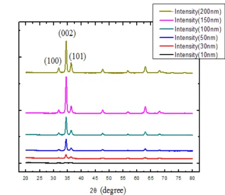
The XRD analysis of different thickness active layer is shown in figure 4-2. The intensity of each diffraction peak becomes larger with thicker films thickness. We found zinc oxide data in JCPDS(Joint of Committee on Powder Diffraction Standards) and compare each diffraction peaks and Bragg angle ( (002) at 2θ=34.421°, (100) at 2θ=31.769°, (101) at 2θ
=36.252°) .We could make sure the films deposited by APP jet are zinc oxide.
We could find out the films show typical polycrystalline zinc oxide properties including strongly preferred (002) orientation and appearing (100) (101) orientation diffraction peaks. (002) orientation is perpendicular to the substrate and along c-axle.
For transparent devices application, we used spectrum implement to measure the transmittance of zinc oxide films on glass substrate. We find the thickness below 100nm films has over 80% transmittance. It is suitable for transparent devices [23]. And we used a function about transmittance and reflectance:
T : Transmittance R : Reflectance
α : Absorption coefficient d : Thickness We used the transmittance and reflectance to calculate the absorption coefficient as shown in figure 4-3. And then we used absorption coefficient to extract the band gap energy of zinc oxide. The band gap of zinc oxide we calculated by absorption coefficient is 3.25eV.
PL analysis of zinc oxide is shown in figure 4-4, we use He-Cr laser (325nm) to be the incident ray hv1 which radiated to the material surface. The laser would arouse electrons jumping to conduction band from valence band. There would appear electron-hole pairs. After a short time, the electrons recombined with holes in valence band. And hv2 as emergent ray
d
e
R
would radiate out from material surface. We can detect hv2 to know the material band gap energy. The band gap energy of zinc oxide which was measured by PL is about 3.26eV because the wavelength of hv2 is 380nm. The results of different measurement methods show near band gap energy. The band gap energy 3.25eV is large enough for transparent material because of the largest energy of visible light is 3.18eV. So the visible light would not be absorbed in zinc oxide. In this way, the electrical properties of devices can work normally in visible light environment.
The ZnO TFTs fabricated with different active layer thickness from 10nm to 200nm had been measured by Agilent 4156C for ID-VG curve and
ID-VD curve as shown in figure 4-5. The gate leakage current was below
10-10A. It controls the off current of devices with 10nm, 30nm, 50nm active layer TFTs. We could find out the devices which had the largest on-off ratio were the TFTs with active layer 30nm and 50nm. The on-off ratios of them are about 107.
But the off current becomes larger with thicker thickness of active layer including 50nm, 100nm, 150nm, 200nm. The reason of off current becoming larger is the leakage current paths and thickness of active layer become larger at the same time when thickness above 50nm. The equivalent resistance is too law when thickness above 50nm. When the thickness of active layer is below 50nm, gate leakage dominates off current as shown in figure 4-6. When the thickness of active layer is above 50nm, the bulk leakage current in zinc oxide dominates off current. The result of electrical properties shows the thickness between 30nm to 50nm is most ideal for on-off ratio. So we measured the ID-VD curve of 50nm active layer devices.
Figure 4-7 shows that total active layer is in depletion state because the drain current does not increase with drain voltage during saturation mode.
We defined some important devices electrical properties:
Threshold voltage(saturation mode): ID=K× (Vg-Vth)2
ID 1/2
=K1/2× (Vg-Vth)
Field effect mobility(saturation mode): K1/2=1/2 × W/L × Cox × Mobility
W/L= 1000µm /100µm Cox=31.85nF/cm2
On-off ratio: Imax/Imin
We extracted threshold voltage and field effect mobility in saturation mode by ID
1/2
-VG curve. The slope of curve in saturation mode is K 1/2
and the intercept on x-axle is threshold voltage. And then we used K1/2 to calculate mobility. The important electrical properties are listed in table 4-1. We can find the mobility of device with 10nm active layer is very small. The XRD analysis of 10nm zinc oxide is shown in figure 4-8. The quality of film become worse because the intensity of (002) peak is weak. We also use the Debye – Sherrer equation to calculate grains size of zinc oxide films:
λ is the wavelength, β is the FWHM, θ is Bragg’s angle
The grains size of 10nm film is 82Å. The grains size of 30nm film is 291Å.The grains size of 50nm film is323Å.The grains size of 10nm film is 356Å.The grains size of 10nm film is smaller than others very clearly because the film is too thin. Grains can not grow maturely and the film shows amorphous structure. Too many grains in zinc oxide would reduce the mobility because of grain boundaries scattering.
Off currents of active layer above 50nm devices become larger than active layer below 50nm devices because of smaller equivalent resistance and more leakage current routes in bulk zinc oxide. On current of TFTs has very little promotion from active layer 30nm to 200nm, but leakage currents have lager promotion. So on-off ratio became smaller with thicker active layer. TFTs with 10nm active layer have very small mobility because of small grains size as shown in XRD results. We chose 50nm to be the thickness of TFTs active layer for ideal on-off ratio.
θ
β
cos
λ
9
.
0
=
D
4.3 Hot plate temperature
The next parameter we discuss is the temperature of hot plate. In many deposition methods, we hope the film to crystallize maturely and to show large grains size so that films deposited by many methods with heating substrates. But high temperature maybe causes thermal damages or some reactions we could not expect. The parameters of hot plate temperature are 100℃, 200℃, 300℃ Figure 4-9 is the I. D-VG curve of different hot plate
temperature. We can find the off current become larger with higher temperature, and the on current shows the same trend but the promotion is smaller than off current very much. A reasonable explanation for the trend of on current is grains size became larger because high temperature made films crystallizing maturely by enough energy.
The SEM images of top view are shown in figure 4-10. Grains size becomes larger with higher temperature and the mobility would increase because of fewer grain boundaries scatterings. So on current becomes larger with higher temperature. The trend is also found in off current, but it is not reasonable to explain that mobility variation dominates the off current. In table 4-2, promotions of field effect mobility with different temperature are not enough to increase off current several orders.
Maybe films deposited on 300 ℃ substrate have more carriers concentration so that the off current becomes larger than low temperature. But threshold voltage of three different temperature devices has no obvious variations. It seems that carriers concentration of zinc oxide has no obvious variations with different temperature parameters.
And then we found a interesting phenomenon in ID-VD curve as shown in figure 4-11. When we discussed about thickness of active layer, 50nm thickness zinc oxide could totally handle in depletion region during devices were in saturation mode. But we found the drain current become larger with drain voltage even in saturation mode. It seems that there are leakage current paths we do not find out. And then we discuss some possible reasons and reasonable explanations.
High temperature in atmosphere-pressure environment would cause reactions we could not expect between samples and air. In this way, impurities or dopants in ZnO would cause defects and traps. Even in depletion region, carriers still could move trap by trap. We make conjectures that the hopping mechanism makes the on and off current becoming larger.
Another reason of increasing on and off current is high hot plate temperature make the grain size and mobility larger, so on and off current become larger . We chose 100 ℃ as hot plate temperature for better stability and larger on-off ratio. Another reason is that low temperature is suitable for flexible electronics.
4.4 Carrier gas
In APP jet systems we have three kinds carrier gas could be chosen including nitrogen, CDA (compressed dry air), and argon. Nitrogen and argon cause similar results in TFTs electrical properties because their activity is not large enough to influence reactions seriously in plasma region.
So nitrogen and argon only have a function as normal inert gas about carrying mists of precursor water solution to plasmas region as normal inert gas. In this way, we chose nitrogen and CDA as carrier gas to discuss because argon is more expensive than nitrogen. Choosing nitrogen to replace argon to be carrier gas is suitable for our cost down principle. We controlled the thickness of active layer being same with different carrier gas. The thickness of active layer is near 50nm.
Figure 4-12 shows very huge difference between nitrogen and CDA. The off current with nitrogen as carrier gas is larger than CDA about five orders. And saturation current of nitrogen as carrier gas is larger than CDA one order. The results show some leakage current paths dominate the off current in nitrogen as carrier gas, but gate leakage current dominates the off current in CDA as carrier gas.
We know the most familiar intrinsic defects in zinc oxide are oxygen vacancies. The oxygen vacancies generate free electrons in zinc oxide, and increasing the carrier concentration. The relationship between resistance and carrier concentration is an inverse ratio. In this way, it seems that the off current with nitrogen as carrier gas increase because carrier concentration increases. The detailed device electric properties are listed on table 4-3. An
indeed evidence is that threshold voltage has very obvious difference between nitrogen and CDA as carrier gas because of the different electrons concentration.
When electrons concentration becomes larger, the threshold voltage will becomes smaller. Therefore we think that the oxygen vacancies in zinc oxide generate free electrons to increase off current. But CDA as carrier gas has an ability to repair oxygen vacancies. So the off current of devices with CDA as carrier gas is smaller than nitrogen very much.
We think the oxygen in CDA can repair oxygen vacancies so that off current is dominated by gate leakage. But CDA contains many different kinds gas including N2 (78%), O2 (21%), Ar (1%), CO2, Ne, He and so on.
For proving oxygen is the key point to influence devices electrical properties, the next parameters we tested are different ratios of oxygen in nitrogen main gas. The carrier gas was still nitrogen.
4.5 Main gas
Several flow rates of oxygen were mixed with main gas, the parameters of main gas are (1)N2 35 SLM (2)N2 35 SLM + O2 120 sccm (3)N2 35 SLM
+ O2 240 sccm(4)N2 35 SLM + O2 360 sccm. The results of electrical
measurement are shown in figure 4-13. There is obvious decrement of off current when oxygen was mixed with main gas. It seems that oxygen causes very large influence to zinc oxide films.
And then we find that gate leakage dominates the off current of devices with oxygen in main gas. The electron concentration becomes smaller because oxygen vacancies are repaired by oxygen in main gas. When electron concentration becomes smaller, the threshold voltage will becomes larger. So table 4-4 shows threshold voltage of devices becomes larger when oxygen is mixed with main gas.
Oxygen causes some influences to mobility as shown in figure 4-14 and to threshold voltage as shown in figure 4-15. We can find some evidences about oxygen vacancies are repaired by oxygen in main gas by PL analysis. When there are defects in material, some trap states will appear between conduction band and valence band. In figure 4-16, the incident ray hv1 radiate to the material surface. The laser would arouse electrons jumping to conduction band from valence band.
There would appear electron-hole pairs. After a short time, the electrons recombined with holes in valence band. And hv2 as emergent ray would radiate out from material surface. We can detect hv2 to know the material band gap energy. If there are many trap states in band gap, the
intensity of hv2 will reduce because electrons are trapped in trap states. Therefore the intensity of hv2 is stronger with the more oxygen ratio as shown in figure 4-17 because defects and oxygen vacancies are repaired. When the flow rates of oxygen are 240sccm and 360sccm, the intensity of
hv2 shows weaker than 120sccm oxygen flow rate. The reason we think is
too much oxygen in zinc oxide causes some defects like oxygen atoms in interstitial sites. Another important influence of oxygen is that mobility decreases from 2.97cm2˙V-1˙S-1 to 1.75cm2˙V-1˙S-1. Figure 4-18 shows that the (002) orientation which has most strong intensity is weaker with more oxygen in main gas. But (110) and (100) orientation peak is stronger with more oxygen in main gas. Oxygen radicals and ions show high activity, so nucleation will emerge in phase plasma region. In this way, particles which are produced during nucleation emerges in phase plasma region will appear in zinc oxide. They are scattering centers and cause that field effect mobility reduces. We can see there are more particles on film surface with more oxygen in main gas in figure 4-19.
Oxygen vacancies could provide free electrons as donors in ZnO. When the concentration of electrons becomes larger, the threshold voltage will become smaller. O2 in main gas can revamp oxygen vacancies in ZnO.
Oxygen radicals and ions have high activity, so nucleation would emerge in phase plasma region. Synthesizing all above-mentioned we chose N2 + 240
sccm O2 to be main gas parameter because of largest on-off ratio. At last we
compare the electrical properties of our devices with best experimental parameters to other devices fabricated by several common methods as listed in table 4-6.