應用於直流至直流切換式電源供應器積體電路設計之先進控制及保護技術
152
0
0
全文
(2)
(3) 應用於直流至直流切換式電源供應器 積體電路設計之先進控制及保護技術 ADVANCED CONTROL AND PROTECTION TECHNIQUES FOR DC-DC SWITCHED MODE POWER SUPPLY IC DESIGN 研 究 生: 馬鳳飛. Student:. Feng-Fei Ma. 指導教授: 吳錦川. Advisor: Jiin-Chuan Wu. 陳巍仁. Wei-Zen Chen. 國 立 交 通 大 學 電子工程學系 電子研究所 博 士 論 文 A Dissertation Submitted to Department of Electronics Engineering and Institute of Electronics College of Electrical and Computer Engineering National Chiao Tung University In Partial Fulfillment of the Requirements For the Degree of Doctor of Philosophy In Electronics Engineering July 2007 Hsinchu, Taiwan, Republic of China. 中華民國九十六年七月.
(4)
(5) 應用於直流至直流切換式電源供應器 積體電路設計之先進控制及保護技術 研究生:馬鳳飛. 指導教授:吳錦川、陳巍仁. 國立交通大學電子工程學系電子研究所. 摘要 在本論文中,我們探討了應用於直流至直流電源轉換的切換式電源供應器。 首先簡單介紹了非隔離式直流至直流切換式電源供應器的基本架構,並且探討了 電源供應器運作上的安全問題,也簡單介紹了電源供應器的設計規格。基於這些 有關直流至直流切換式電源供應器的基本知識,我們開發了數種電路技術。這些 電路技術提高了能量轉換效率、縮小電源供應器體積並且可以操作在相當廣的範 圍。此外,這些電路技術也提供了快速瞬變反應以及安全的操作。我們將這些新 開發的技術以一個單晶片電流模式控制的降壓轉換器來實現。這些電路技術可以 被應用到其它架構如昇壓或昇降兩用型的切換式電源供應器設計,特別是應用於 積體電路電源轉換器設計上。. 我們提出了一個可整合於單晶片上的柔性啟動電路,它並不需要額外的針腳 並且只佔了很小的晶片面積。這個電路以串聯金氧半電晶體及一個內建於晶片上 的小電容來達到數毫秒到數十毫秒的柔性起動時間。此柔性啟動電路可以防止電 源供應器啟動時的突波電流,並且在縮小電源供應器體積的同時仍保障了安全 I.
(6) 性。此電路的另一好處是它非常簡單,因此可以很容易應用於其它的電源供應積 體電路設計。. 另外,我們也提出了動態部分停工策略,這個策略充分利用了切換式電源供 應器的特性。它降低了對輸入電流的浪費,同時卻仍保持電路的性能。此動態部 分停工策略提昇了轉換效率,特別是在輕載的時候。因此由電池供電的設備其待 機時間可因應用此策略而拉長。根據我們的實驗,當此策略與突波頻率調變共同 使用時,其轉換效率可由 62 % ~ 75 %提昇至 84 % ~ 89 %。. 在我們的設計中,我們採用了一種基於電流傳送器的近無功耗電流感測技術 來實現我們的電流模式控制。我們也充分利用了這個電流感測技術的特性而開發 了新的斜率補償電路和過電流保護電路。我們所提出的斜率補償電路較傳統電路 而言大幅降低了電路的複雜度,因此節省了晶片面積。在此同時,也因為減少了 訊號轉換的次數而降低了訊號的失真。至於過電流保護電路也較傳統電路大為簡 化。此過電流保護電路的特長為面積小、功耗低及反應速度快,因此可確保電源 供應器的安全性。此外,所提出的斜率補償電路和過電流保護電路都很容易因應 不同的需求來加以設計並調整,因此對切換式電源供應器而言,我們可以得到很 好的電壓調節並且能適用於廣泛的操作範圍。對於不同的切換式電源供應器架構 也能適用。. 這些技術加上一些基本的保護電路都整合於一個示範性晶片上。根據量測結 果,我們可以得知這些技術確實發揮了它們的功效。在此我們提出了一個最高可 達 96.7 %轉換效率的單晶片直流至直流電流式控制降壓轉換器。我們提出了以較 低功耗達到快速電路反應的動態部分停工策略以增進轉換效率。突波寬度調變和 突波頻率調變的自動切換並配合動態部分停工策略更進一步提昇了輕載時的轉 換效率。電流偵測電路和斜率補償電路則簡化了電流式控制電路並加快了反應速 度。一個高速過電流保護電路也根據此電流偵測電路而發展出來。新的整合式柔 II.
(7) 性啟動電路不需額外元件就能有效地防止啟動時的突波電流。我們設計的直流至 直流轉換器已採 0.6 微米的互補式金氧半製程製作出來,晶片面積為 1.35 毫米平 方,而控制器部分佔 0.27 毫米平方。實驗結果顯示此新式柔性啟動電路具有 1.5 毫秒以上的柔性啟動時間,因此有效地抑制了啟動時的突波電流。此轉換器可在 2.2 至 6 伏特的輸入電壓下操作,切換頻率為 1.1 百萬赫。在輸出電流為 0.9 至 800 毫安培時具有 88.5 ~ 96.7 %的轉換效率,而在輸出電流為 1000 毫安培時仍 有 85.5 %的轉換效率。. III.
(8) IV.
(9) ADVANCED CONTROL AND PROTECTION TECHNIQUES FOR DC-DC SWITCHED MODE POWER SUPPLY IC DESIGN STUDENT: FENG-FEI MA. ADVISOR: JIIN-CHUAN WU, WEI-ZEN CHEN. DEPARTMENT OF ELECTRONICS ENGINEERING AND INSTITUTE OF ELECTRONICS NATIONAL CHIAO TUNG UNIVERSITY. ABSTRACT In this dissertation, we discuss about the switched mode power supply (SMPS) for DC-DC power conversion. Basic topologies of non-isolated DC-DC SMPS are introduced. Safety considerations for power supply design are discussed. The design specifications are also included. Based on the knowledge of DC-DC SMPS, we developed several new circuit techniques to achieve high conversion efficiency, compact converter size, wide operating range, fast transient response and safety operation. These developed circuit techniques were realized in a monolithic current-mode buck converter. The application of these circuit techniques can be extended to other topologies like boost and buck-boost of SMPS design, especially in integrated circuit power converter design.. The on-chip soft-start circuit occupies a small silicon area and eliminates the need of extra pin-out. This circuit achieves one to tens of milliseconds soft-start time V.
(10) using series MOS transistors and a small on-chip capacitor. This circuit prevents the inrush current during the start-up of the power module. It provides safety operation and shrinks the converter size in the same time. Another benefit of the proposed circuit technique is that because of its simplicity, it can be easily adopted for any other power supply IC design.. The dynamic partial shutdown strategy (DPSS) is a power management strategy. By exploiting the switching characteristics of SMPS, we developed this strategy. This strategy eliminates the unwanted waste of operating current and keeps the circuit performance at the same time. The DPSS improves the conversion efficiency especially in light load operation. Thus the standby time of battery operated devices can last longer by utilizing DPSS. Combined with the pulse frequency modulation (PFM) mode, the conversion efficiencies are improved from 62 % ~ 75 % to 84 % ~ 89 % measured in our test chip.. In our design, we choose a quasi-lossless current conveyor based current sensing technique to implement our current-mode control. By exploiting the characteristics of this current sensing technique, we developed the slope compensation circuit and the over-current protection circuit. The proposed slope compensation circuit has reduced circuit complexity than traditional ones thus the silicon area is saved. The signal distortion is also reduced because we eliminate the multi-conversions of signals. The over-current protection is also simpler than traditional ones. The benefits of the over-current protection circuit are reduced silicon area, reduced power consumption and faster response for safety operation. Additionally, these circuits can be easily designed and adjusted. So we can achieve good regulation and wide operating range. These circuit techniques can also be applied to other topologies for different. VI.
(11) applications.. Incorporating with other basic protection schemes, the above techniques are integrated into a demo chip. From the measurement results, we can see the effectiveness of these developed techniques. A monolithic current-mode pulse width modulation (PWM) step-down DC-DC converter with 96.7% peak efficiency is presented. The high efficiency is achieved by DPSS which enhances circuit speed with less power consumption. Automatic PWM and PFM switching boosts conversion efficiency during light load operation. The modified current sensing circuit and slope compensation circuit simplify the current-mode control circuit and enhance the response speed. A simple high-speed over-current protection circuit is proposed with the modified current sensing circuit. The new on-chip soft-start circuit prevents the power on inrush current without additional off-chip components. The DC-DC converter has been fabricated with a 0.6 μm CMOS process and measured 1.35 mm2 with the controller measured 0.27 mm2. Experimental results show that the novel on-chip soft-start circuit with longer than 1.5 ms soft-start time suppresses the power-on inrush current. This converter can operate at 1.1 MHz with supply voltage from 2.2 V to 6.0 V. Measured power efficiency is 88.5 ~ 96.7% for 0.9 mA to 800 mA output current and over 85.5% for 1000 mA output current.. VII.
(12) VIII.
(13) 致謝 『耶和華是我的牧者;我必不致缺乏。祂使我躺臥在青草地上,領我在可安 歇的水邊。祂使我的魂甦醒,為自己的名引導我走義路。我雖然行過死蔭的幽谷, 也不怕遭害,因為你與我同在;你的杖,你的竿,都安慰我。在我敵人面前,你 為我擺設筵席;你用油膏了我的頭,使我的福杯滿溢。我一生一世必有恩惠慈愛 隨著我,我且要住在耶和華的殿中,直到永遠。』(聖經 詩篇二十三篇). 『這不是說,我已經得著了,或已經完全了,我乃是竭力追求,或者可以取 得基督耶穌所以取得我的。弟兄們,我不是以為自己已經取得了,我只有一件事, 就是忘記背後,努力面前的,向著標竿竭力追求,要得神在基督耶穌裏,召我向 上去得的獎賞。』(聖經 腓立比書三章 12~14 節). 感謝主耶穌一路帶領我、保守我,在每一天、每一件事上都看顧我,帶領我 完成學業,並使我生命長大。. 感謝我的指導老師吳錦川教授,在學業上的指導以及生活上的關心。也感謝 陳巍仁教授在最後一年給予許多幫助。. 感謝奈米電子與晶片系統實驗室的學長、同學、學弟妹及助理們給予的一切 幫助。. 感謝致新科技股份有限公司的主管及同事們,在技術上及實作上給予很多幫 助。特別感謝楊人仰學長在電路設計及實作上許多寶貴的建議。. 感謝每一位關心我、為我代禱的聖徒。非常謝謝你們,因著你們的扶持,使 我能與你們一同領略何為那闊、長、高、深。. IX.
(14) 感謝我的父親、母親、姊姊、妹妹以及我的妻子于梅、女兒心樂,謝謝你們 一路上的愛和支持。. 感謝這一路上每一位曾經幫助過我的人,謝謝你們。 馬鳳飛. X.
(15) TABLE OF CONTENTS. 摘要................................................................................................................................ I ABSTRACT .....................................................................................................................V 致謝............................................................................................................................. IX TABLE OF CONTENTS ................................................................................................. XI LIST OF TABLES ......................................................................................................... XV LIST OF FIGURES ..................................................................................................... XVI. 1. INTRODUCTION .................................................................................... 1 1.1. BACKGROUND ........................................................................................1. 1.2. LOW POWER DC-DC CONVERSION .....................................................3. 1.3. TRENDS AND CHALLENGES OF DC-DC CONVERTER DESIGN .............4 1.3.1. High Efficiency..............................................................................5. 1.3.2. Compact Size .................................................................................5. 1.3.3. Low Output Voltage and Low Noise .............................................6. 1.3.4. Wide Operating Range...................................................................6. 1.3.5. Fast Transient Response ................................................................6. 1.3.6. Safety Operation ............................................................................7. 1.4. MOTIVATION .........................................................................................7. 1.5. RESEARCH GOALS AND CONTRIBUTIONS .............................................9 XI.
(16) 1.6. THESIS ORGANIZATION.......................................................................11. 2. SWITCHED MODE DC-DC POWER SUPPLY BASICS ......................... 13 2.1. REGULATED DC POWER SUPPLIES.....................................................13 2.1.1. Linear Regulated Power Supplies................................................15. 2.1.2. Switched Mode Power Supplies ..................................................16. 2.2. BASIC CONVERTER TOPOLOGIES .......................................................18 2.2.1. Buck .............................................................................................18. 2.2.2. Boost ............................................................................................20. 2.2.3. Buck-Boost ..................................................................................22. 2.2.4. Synchronous Rectification ...........................................................24. 2.3. MODULATION TECHNIQUES ................................................................24 2.3.1. Pulse Width Modulation (PWM) .................................................24. 2.3.2. Pulse Skip Modulation (PSM) .....................................................25. 2.3.3. Pulse Frequency Modulation (PFM)............................................26. 2.4. PROTECTIONS OF SMPS .....................................................................27 2.4.1. Over-Current Protection...............................................................27. 2.4.2. Over-Voltage Protection ..............................................................28. 2.4.3. Inrush Protection..........................................................................28. 2.4.4. Device Protection.........................................................................30. 2.4.5. Over Temperature Protection.......................................................30. 2.5. PERFORMANCE SPECIFICATIONS ........................................................30 2.5.1. Efficiency.....................................................................................31. 2.5.2. Input Voltage Range ....................................................................31. 2.5.3. Load Regulation...........................................................................32. 2.5.4. Line Regulation............................................................................32. XII.
(17) 2.5.5. Transient Response ......................................................................33. 2.5.6. Electromagnetic Interference (EMI) ............................................34. 3. A MONOLITHIC CURRENT-MODE BUCK CONVERTER WITH ADVANCED CONTROL AND PROTECTION CIRCUITS ......................... 35 3.1. INTRODUCTION ....................................................................................35. 3.2. STRUCTURE OF THE MONOLITHIC BUCK CONVERTER .....................37 3.2.1. PWM ............................................................................................37. 3.2.2. PFM..............................................................................................38. 3.2.3. Automatic PWM/PFM Mode Switching .....................................40. 3.2.4. The Proposed Converter ..............................................................41. 3.3. DESIGN CONSIDERATIONS AND CIRCUIT IMPLEMENTATIONS...........42 3.3.1. On-Chip Soft-Start Circuit...........................................................42. 3.3.2. Dynamic Partial Shutdown Strategy (DPSS)...............................45. 3.3.3. Current Sensing and Slope Compensation...................................49. 3.3.4. Over-Current Protection...............................................................54 EXPERIMENTAL RESULTS ..................................................................57. 3.4. 3.5. 3.4.1. Soft-Start ......................................................................................58. 3.4.2. Efficiency.....................................................................................59. 3.4.3. Steady State and Transient Response ..........................................59. 3.4.4. Over-Current Protection...............................................................60. 3.4.5. Comparison ..................................................................................60 CONCLUSION ......................................................................................61. 4. PRACTICAL DESIGN AND LAYOUT CONSIDERATIONS ...................... 75 4.1. INTRODUCTION ....................................................................................75. 4.2. DESIGN CONSIDERATIONS...................................................................76 XIII.
(18) 4.2.1. Protection Functions ....................................................................76. 4.2.2. Dead Time Control ......................................................................79. 4.3. LAYOUT CONSIDERATIONS .................................................................80 4.3.1. Grounding of SMPS ICs ..............................................................81. 4.3.2. Gate Routing of Power Transistors..............................................83. 4.3.3. On-Resistance of Power Switches ...............................................86. 5. CONCLUSION AND FUTURE WORK .................................................... 91 5.1. CONCLUSION .......................................................................................91 5.1.1. On-Chip Soft-Start Circuit...........................................................91. 5.1.2. Dynamic Partial Shutdown Strategy (DPSS)...............................92. 5.1.3. Current Sensing, Slope Compensation and Over-Current Protection .....................................................................................92. 5.2. FUTURE WORK ....................................................................................93. REFERENCES................................................................................................................95 APPENDIX...................................................................................................................107 學經歷資料表 ...........................................................................................................127. XIV.
(19) LIST OF TABLES. Table 3.1. List of component values used in test setup.........................................58. Table 3.2. Summary of performance ....................................................................72. Table 3.3. Performance comparison .....................................................................73. Table 4.1. Comparing measurement and simulation results of the on-resistance of the power transistors. ...........................................................................86. XV.
(20) LIST OF FIGURES. Fig. 1.1. Voltage-mode control in SMPS .........................................................8. Fig. 1.2. Current-mode control in SMPS .........................................................8. Fig. 2.1 (a). Series regulated power supply. ........................................................14. Fig. 2.1 (b). Shunt regulated power supply..........................................................14. Fig. 2.2 (a). Principle of linear series regulator. ..................................................15. Fig. 2.2 (b). Principle of linear shunt regulator....................................................16. Fig. 2.2 (c). Principle of switching series regulator.............................................17. Fig. 2.2 (d). Principle of switching shunt regulator. ............................................17. Fig. 2.3. Buck converter topology and related waveforms. ...........................19. Fig. 2.4. Boost converter topology and related waveforms. ..........................21. Fig. 2.5. Buck-boost converter topology and related waveforms. .................23. Fig. 2.6. Switching signal of pulse width modulation (PWM). .....................24. Fig. 2.7. Output waveform and switching signal of pulse skip modulation (PSM)...............................................................................................25. Fig. 2.8. Output waveform and switching signal of pulse frequency modulation (PFM)............................................................................26. Fig. 2.9. A typical soft-start circuit used in a PWM control circuit aids the gradual increase of the PWM signal to its operating value. ............29. Fig. 3.1. Simplified structure of current-mode PWM control........................38. Fig. 3.2. Simplified structure of PFM control. ...............................................39. XVI.
(21) Fig. 3.3. Functional block diagram of the developed monolithic buck converter. .........................................................................................41. Fig. 3.4. Soft-start ramp generator. ................................................................44. Fig. 3.5. DPSS in PWM mode. Blocks with horizontal lines are shut down when high side PMOS is turned on. Blocks with vertical lines are shut down when low side NMOS is turned on. ...............................47. Fig. 3.6. DPSS in PFM mode. Blocks with horizontal lines are shut down when high side PMOS is turned on. Blocks with vertical lines are shut down when low side NMOS is turned on. Blocks with oblique lines are shut down when both power transistors are turned off......48. Fig. 3.7. Current-conveyor-based sense-FET current sensing. ......................50. Fig. 3.8 (a). Adding compensation ramp and sensed inductor current signal. (a) Summing amplifier. .........................................................................52. Fig. 3.8 (b). Adding compensation ramp and sensed inductor current signal. (b) Use two V-to-I converters and adding the current signals by a resistor..............................................................................................52. Fig. 3.8 (c). Adding compensation ramp and sensed inductor current signal. (c) Proposed summing circuit................................................................54. Fig. 3.9 (a). Over-current protection circuit. (a) Conventional over-current protection circuit. .............................................................................55. Fig. 3.9 (b). Over-current protection circuit. (b) Proposed over-current protection circuit. ..............................................................................................56. Fig. 3.10. Chip microphotograph. ....................................................................57. Fig. 3.11. Experimental setup of the monolithic buck converter. ....................58. Fig. 3.12. Simulated waveforms of input current and output voltage during start-up with 2.5 Ω load (about 1000 mA at steady-state)...............62 XVII.
(22) Fig. 3.13 (a) (b) Measured input current and output voltage during start-up. From top to bottom: Channel 3 is chip enable, Channel 1 is output voltage and Channel 4 is input current. (a) No load. (b) 12.5 Ω load (about 200 mA at steady-state). .........................................................................63 Fig. 3.13 (c) (d) Measured input current and output voltage during start-up. From top to bottom: Channel 3 is chip enable, Channel 1 is output voltage and Channel 4 is input current. (c) 5 Ω load (about 500 mA at steady-state). (d) 2.5 Ω load (about 1000 mA at steady-state). .......64 Fig. 3.14 (a). Measured conversion efficiency. (a)VIN = 3.6 V and VOUT = 2.5 V. 65. Fig. 3.14 (b). Measured conversion efficiency. (b)VIN = 4.2 V and VOUT = 2.5 V.65. Fig. 3.15. Steady-state waveforms of PFM mode operation. From top to bottom: Channel 1 is output ripple voltage (AC coupled), Channel 4 is inductor current and Channel 2 is switch node LX. (a) 10 mA load. (b) 20 mA load. ................................................................................66. Fig. 3.16. Steady-state waveforms of the output ripple voltage (Channel 1, AC coupled) and the switch node LX (Channel 2) in PWM mode. (a) Duty cycle > 50%. (b) Duty cycle < 50%........................................67. Fig. 3.17. 500 mA step load-transient response. Channel 1 is output voltage (AC coupled) and Channel 2 is output current (step from 200 mA to 700 mA and from 700 mA to 200 mA)............................................68. Fig. 3.18. Over-current protection test. From top to bottom: Channel 1 is output voltage (DC coupled), Channel 4 is inductor current and Channel 2 is switch node LX. (a) Normal operation with 2.5 (about 1000 mA) load. (VOUT = 2.5 V) (b) The converter is over-loaded (RLOAD = 1 Ω). The peak inductor current is limited to 1.28 A and the output voltage falls from 2.5 V to about 1.2 V. (c) XVIII.
(23) Increasing the load demand (RLOAD = 0.5 Ω) causes output voltage to fall to about 0.6 V but the peak inductor current is still limited to 1.28 A. (d) Further load demand (RLOAD = 0.33 Ω) causes output voltage to fall to about 0.4 V but the peak inductor is still limited to 1.28 A...............................................................................................70 Fig. 4.1. Over temperature detector................................................................77. Fig. 4.2. The inductor current waveform of a buck converter when VOUT is short to ground. ................................................................................78. Fig. 4.3. Dead time control using biased inverters to sense the gate voltage of power transistors. .............................................................................79. Fig. 4.4. Current waveforms of the power ground and the input of a buck converter that cause bouncing at both power ground and VIN. ........81. Fig. 4.5. Ground bouncing of “power ground” that cause false conduction of the power transistor..........................................................................82. Fig. 4.6. S-shaped gate routing of power transistor for reducing ground bounce. .............................................................................................84. Fig. 4.7. Improving accuracy of current sensing by Kelvin connection. .......85. Fig. 4.8. Examples of power transistor layout. On-resistance: (a) ≈ (b) > (c)89. XIX.
(24) XX.
(25) CHAPTER 1 INTRODUCTION 1.1. BACKGROUND The discovery of electric power changes our life. Different types of energy such. as heat energy, potential energy, kinetic energy and other types of energies, can be transformed to electric power. This makes the storage, the transportation and the transformation of energy easier. Through many years, people invent devices that utilize electric power. The supply lines stretch into buildings so that the usage of electric power becomes more convenient. The batteries, which store the electrical energy, make the portable devices popular. Today, we use electrical energy everywhere in our daily life.. Power electronics is an established technology that bridges the power industry with its need for fast controllers, and the semiconductor industry with its attempt to produce devices with greater power handling capabilities. In essence, what power electronics does is to condition the power from a supply to suit the needs of the load.. Power conditioning is known also as power modulation or power conversion. This conditioning may take a specialized form such as the regulation of voltage, or the conversion of alternating current (AC) to direct current (DC), or the conversion of direct current to alternating current.. 1.
(26) There is no one configuration of the power electronics system to satisfy all types of conditioning. This becomes evident as a number of systems are considered. Indeed, the conversion of one given type of supply (usually specified by voltage and frequency) into any other type of supply has to be designed on its own merits.. All electronic circuits need a supply of power. For low power consumption units or for portable operation, a battery is often used – a solar cell may even be enough. Higher power circuits are normally powered from the AC mains supply. In almost all cases the power requires conversion to the appropriate DC voltage by an electronic power unit, which is usually switched mode in operation.. Over the past 20 years, there have been significant changes in the design of power supplies. The most important of these has been the widespread change from linear power supplies to those that operate on a switching basis – so called Switched Mode Power Supplies (SMPS). The principal reason for the move to SMPS is their much greater efficiency – typically 80-90 % as opposed to 30-40 % for linear units. This greatly reduces the cooling requirements, and allows a much higher power density. [1]-[13]. The concept of high frequency switching of transistors to provide a controllable DC output has been around for some time. What has allowed the widespread adoption of SMPS technology has been the availability of a range of suitable active and passive components. The advent of MOSFETs with high power rating has been a particularly important advance, together with the availability of high-speed diodes and improved magnetic materials. Now circuits can be designed to operate at switching frequencies into the megahertz range, with consequent reductions in cost and in volume of the power supply. 2.
(27) Advances in power supply design and manufacture have had to keep pace with advances in the electronic systems they supply. The requirement for portability has led to demands for more compact units with reduced losses, and the trend towards lower operating voltages has proved particularly demanding. In addition, regulations relating to safety and electromagnetic compatibility are becoming increasingly more stringent. Designers and production engineers have proved to be up to the task and a wide range of innovative techniques are now standard in the electronic power supply industry. Size and unit costs have been reduced while reliability has been increased. Efficiency has been improved by the use of new active components, new circuit topologies and new ways of manufacture.. 1.2. LOW POWER DC-DC CONVERSION Although the power electronics include so many interesting topics that can be. studied, we can only focus on a small part of them. In this thesis, we will discuss about lower power DC-DC conversion, especially switched mode conversions.. The rapid advances in computer, communications, and consumer electronics technology are having a major impact on our everyday life. This trend has been largely due to recent advances in emerging VLSI and ULSI semiconductor technology. Most of these integrated circuits need a DC power supply, but usually in different voltage levels. In most cases, we have only one power source – An adaptor or a battery. Thus we have to consider the need of DC-DC conversions as follows.. The demands for higher functionality, smaller device size, and lower power dissipation have brought new technological issues. They can be resolved using more advanced semiconductor processes to implement the so-called system-on-a-chip 3.
(28) (SOC). The processes have been improved from 0.35 μm to 0.25 μm, 0.18 μm, 0.13 μm, 90 nm, 65 nm and even smaller for commercial products. By utilizing these advanced processes, more circuits can be implemented into one single chip and system size and complexity are greatly reduced. As the dimension of transistor continues to shrink, the gate oxide thickness of MOSFET also becomes thinner. To prevent electric breakdown, the maximum allowable supply voltage has dropped with each generation of semiconductor technology. For example, it is 3.3 V for 0.35 μm technology and 1.8 V for 0.18 μm technology. The operating voltage of an integrated circuit requires scaling down in order to maintain the reliability.. Another reason to perform DC voltage conversion is supply voltage boosting in portable equipment especially for lightning the screen. Small size and light weight portable equipments such as notebook computers, cellular phones, digital cameras, MP3 players and personal digital assistants (PDA) provide convenient data access, communication and entertainment functions. The size and weight limitations restrict the number of battery cells. Thus, the input voltage provided by the batteries may be lower than the required supply voltage. Step-up voltage conversions are required at this time. Considering the above cases, we need multiple DC-DC converters to generate sufficient outputs to fit the need.. 1.3. TRENDS AND CHALLENGES OF DC-DC CONVERTER DESIGN Today, high performance, long operating time, compact size and low cost are. essential factors of a successful electronic product. For example, it is expected a smart phone can process extensive multimedia data with standby time of a week and size of 4.
(29) the palm. These requirements challenge traditional power supply control techniques and converter design. In this section, trends and challenges of DC-DC converter design are described.. 1.3.1. High Efficiency. While transistor numbers inside a single chip continues to double every 18 months as Moore’s Low predicts, energy density of batteries has increased little. Conversion efficiency is particularly important in battery-powered equipments. Improving conversion efficiency can directly prolong the operating time of portable devices with the battery capacity unchanged. Higher conversion efficiency also helps to reduce the unwanted heat generation. Lower heat production saves space for heat ventilation. Advanced power management techniques and converter circuits design will help to extend battery life and shrink device size.. 1.3.2. Compact Size. Reducing size and weight is one of the major demands of portable devices. In addition to improving efficiency, we need to consider other ways to reduce the space and weight occupied by power converters.. Generally, switched mode converters are composed of many discrete components that occupy large space. Since physical size minimization is a major design objective in portable devices, reductions of external component counts and size are trends of SMPS design [14]-[15]. Significant energy is dissipated in the parasitic impedances of external interconnection and components [16]. Therefore, integrating external components decreases energy loss. Higher switching frequency can reduce. 5.
(30) the required sizes of filter inductor and capacitor and also improve efficiency [17]. Further physical size minimization can be made by integrating controller into other circuits [18]-[19].. 1.3.3. Low Output Voltage and Low Noise. In portable and high performance systems, electronic systems are designed to operate at the optimal supply voltage [20]. Low operating voltage of new generation integrated circuit has set tight tolerance of converter’s output. Communication and audio circuits are also sensitive to noise interference. Low output ripple and low noise are essential. Fast transient response is required to prevent large output deviation during step load transient. In addition, fixed frequency operation of switched mode converters is favorable, because it is easier to filter out switching noise.. 1.3.4. Wide Operating Range. Many portable devices can be powered by multiple input sources such as AC adapter and battery. These power sources may have different voltage levels. Besides, the voltage of a battery can vary significantly from full charged state to run out of stored electrical energies. The DC-DC power converters must operate under these conditions and keep the output voltage well regulated. All the circuits of the converter controller and the power switches must have a wide operating range to ensure safety and stable operation of the devices supplied by the converter.. 1.3.5. Fast Transient Response. Microprocessors today exhibit much heavier load and faster current slew rate. Advanced power management techniques are usually adopted. When the system is in 6.
(31) sleep mode, come circuits are shut down and operating voltage is scaled down in order to minimize standby current. The most challenging issue comes from step load transients when the system transits from sleep mode to full loading mode. These two modes correspond to minimum and maximum loading conditions respectively. The regulator has to maintain output voltage within tight tolerance during this fast slew-rate transient. These power requirements have become new challenges. [21]-[25]. 1.3.6. Safety Operation. System designers naturally wish to avoid any system faults occurring due to the power supply, so the specifications for the power supply normally include large safety margins. As the power supply will have its own safety margins, it is often grossly over-specified, and as a result is considerably larger, heavier and more expensive than is necessary.. On the other hand, any electronic system requires a power source in order to function correctly, yet the power supply is normally the most neglected part of the complete system. It is often hastily designed (or bought in) after the rest of the system is complete, and placed in the leftover space, which is often too small and has inadequate ventilation for cooling purposes. How to provide safety operation using simplest circuits and occupying least space is one of the challenges of power converter design.. 1.4. MOTIVATION As described in section 1.3, a desirable DC-DC converter has high efficiency,. compact size, wide operating range, fast transient response and can operate safely. 7.
(32) Fig. 1.1. Voltage-mode control in SMPS. There are many control methods and circuits developed to meet these requirements. But each one has some disadvantages. For example, voltage-mode control is one of the commonly used control method in SMPS (Fig. 1.1). Design of this control scheme is simple and straightforward. It has only one feedback loop and is easier to design and analyze. The output voltage is controlled by directly changing the duty ratio. Therefore, this control scheme is also called direct duty control. It can provide good noise margin if you use a large amplitude ramp in determining the duty ratio. It also has low impedance output and can provide good line regulation, load regulation and even cross regulation for multiple outputs. However, its application is limited because any change in line or load must first be sensed as an output change and then corrected by the feedback loop. This usually means slow response. Another disadvantage is that the output filter adds two poles to the control loop. We need to add a dominate-pole in much lower frequency or add a zero to compensate it. The loop gain varies with the input voltage also makes the compensation difficult.. Fig. 1.2. Current-mode control in SMPS. 8.
(33) Another popular method is current-mode control, which is also called current programmed control and current injected control, was introduced in 1978 [26]-[35] (Fig. 1.2). Since the inductor current rises with a slope determined by input and output voltages, this waveform will respond immediately to line voltage changes, eliminating both the delayed response and gain variation with changes in input voltage. This control scheme utilizes dual loops to control both output voltage and inductor current. It effectively eliminates the phase lag of the filter inductor and makes loop compensation easier. Since the current information is sensed cycle-by-cycle, we can see an additional benefit of easier cycle-by-cycle current limiting. The current-mode control has shown more attractive characteristics than voltage-mode. However, current sensing elements not only require additional circuitry but also reduce efficiency. Moreover, switching noise can easily corrupt the sensed current signal. Therefore, instability caused by noise is common in a current-mode system [36]-[37]. Instability problem also occurs at very low duty ratio caused by high input voltages and low output voltages.. There are still many other methods of implementing SMPS. All these circuits have their own advantages and disadvantages. We choose current-mode control as our start point and try to investigate the possibility of eliminating the disadvantages. We want to find a way that a high efficiency, compact size and safely operated SMPS can be easily designed for different applications.. 1.5. RESEARCH GOALS AND CONTRIBUTIONS As being power electronics engineers, providing good quality electrical power is. our responsibility. How to improve the quality of supplied power with lower cost is. 9.
(34) our research goal.. Fast response, tight regulation, high efficiency, high stability,. compact size and safety operation are the key factors of a high performance power converter. We focus on the integrated circuit implementations. We had implemented a monolithic current-mode buck converter using the new developed control and protection circuits. All the developed techniques can be reused in the SMPS IC design for other applications. The original contributions of this work are in three main points.. First, the on-chip soft-start circuit which occupies small silicon area and do not need extra pin-out. This circuit helps to protect the power source and the converter itself at the very beginning of the power on of the converter. It eliminates the inrush current when the converter is powered on. The inrush current may cause severe voltage drops at the power source and may cause the system faults or other damages to the power source, the circuit directly powered by the power source and the converter. Traditional circuit utilized a big capacitor or other costly circuit to do soft-start. Our approach using a simple circuit and only occupies a very small silicon area to achieve the same function as well as the traditional circuits.. Second, the Dynamic Partial Shutdown Strategy (DPSS), which increases the conversion efficiency especially in light load operation. The power conversion efficiency is very important especially for portable devices that utilize batteries as their power sources. The DPSS successfully reduces the operating current wasted by the control circuits. The efficiency is improved especially in light load operation. This means a longer standby time can be achieved using this strategy.. Third, the slope compensation and the over-current protection circuits which take advantage of the existing current sense method. As described in section 1.4, the current sense circuits usually cause power loss and greatly reduce the conversion 10.
(35) efficiency. We choose a quasi-lossless current sense circuit to improve the efficiency in the current-mode control. At the same time, the current sense circuit helps the development of the new slope compensation and over-current protection circuits. Although the compensation of current-mode control has more flexibility, it is not easy to implement a stable current-mode SMPS because of its inseparable dual feedback loop. The slope compensation in the current-mode control was developed for stabilize the current-mode converter. Traditional methods of implementing slope compensation are complex and may induce signal distortion in the control loop. We proposed a simple circuit to improve the slope compensation. The new over-current protection circuit also takes advantages of the current sense circuit. This simple circuit provides fast response to ensure safety operation under over-loaded conditions by very low power consumption.. 1.6. THESIS ORGANIZATION In this thesis, we introduce the basics terms of the switched mode DC-DC power. supplies in chapter 2. Some fundamental topologies of a switched mode DC-DC power supply like buck, boost and buck-boost are introduced. The modulation schemes of SMPS are briefly listed. The specifications of SMPS give us an evaluation standard of the performance of the SMPS.. In chapter 3 we demonstrate the advanced control and protection circuits in a monolithic current-mode buck converter. The newly developed strategies and circuits are discussed in this chapter. All of them can be easily adopted for integrated SMPS in different topologies and for different applications. The on-chip soft-start circuit, the dynamic partial shutdown strategy, the current sense circuit, the slope compensation. 11.
(36) circuit and the over-current protection circuit are all realized in this monolithic converter. The performances are measured to show the practicability and effectiveness of them. We can see a compact size, high efficiency and well-protected converter illustrated in this chapter.. Chapter 4 presents the practical considerations in circuit design and silicon layout of a power converter integrated in single chip. Many practical issues such as switching noise, on-resistance of integrated power switches and some other protection considerations are discussed. These issues seem unimportant, but they may cause unstable operation, performance degradation and even destroy the converter or the system. In this chapter, we deal with these issues and give practical suggestions according real experience.. Chapter 5 concludes this work and tries to suggest for future works.. 12.
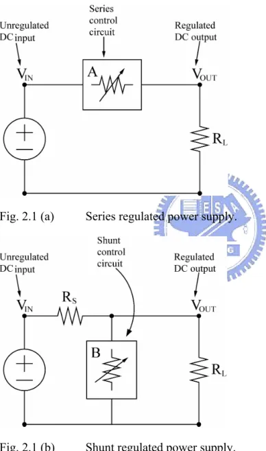
(37) Chapter 2 SWITCHED MODE DC-DC POWER SUPPLY BASICS 2.1. REGULATED DC POWER SUPPLIES There are two basic ways of maintaining a fixed output voltage in a DC power. supply, i.e. by series and shunt regulators [5].. The principle of the series regulator is illustrated in Fig. 2.1 (a). Here you have an unregulated DC input, VIN, feeding through a series-control circuit, A, to give a fixed regulated DC output, VOUT. The series-control circuit works by adjusting the voltage drop from input to output to keep a constant voltage at the output. This variable series voltage drop takes up both variations in the input voltage, and varying voltage drops inside the system arising from changing load currents. The variable resistor symbol in the circuit block, A, emphasizes that the series regulator works like a variable resistor in series with the load, adjusting itself to keep the output voltage across the load constant.. The shunt regulator works on a different principle, illustrated in Fig. 2.1 (b). Here an unregulated DC input feeds a current through a series resistor, RS, to give a lower DC voltage across the load resistor RL. The shunt-control element, B, draws current from the output rail, as does, of course, the load RL. The shunt-control element adjusts the current it takes so that the voltage drop across the series resistor RS varies. 13.
(38) to keep the output rail voltage, VOUT, unvarying under changes of load resistance and unregulated input voltage, VIN. Once again the control element can be seen to work like a varying resistor as indicated by the symbol in the shunt circuit block, B, in the diagram.. Fig. 2.1 (a). Series regulated power supply.. Fig. 2.1 (b). Shunt regulated power supply.. In essence, the series regulator soaks up changes in the voltage drop from the input supply onward to the output, while the shunt regulator soaks up current variations in the load. In each case the net result is the same: the output voltage is regulated, i.e. held constant, at a fixed value. 14.
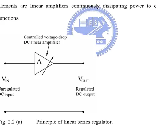
(39) In nowadays, there are mainly two types of regulated DC-DC power supplies. One of them is linear regulated power supply and another is switched mode power supply.. 2.1.1. Linear Regulated Power Supplies. Linear regulated power supplies is a simple, widely used DC-DC regulator. In linear regulators, the controlled resistor (series or shunt) elements described above continuously dissipate some power in keeping the output voltage constant under varying input voltage and output load conditions. Fig. 2.2 (a) and (b) show once again series and shunt regulator systems, but this time they emphasize that the control elements are linear amplifiers continuously dissipating power to carry out their functions.. Fig. 2.2 (a). Principle of linear series regulator.. The linear regulators have many desirable characteristics such as low output ripple, good line and load regulation, fast transient response and low electromagnetic interference (EMI). How low efficiency limits their application. When it comes to high volt-amp requirements or transformerless high-step-down voltage between input. 15.
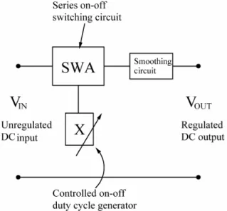
(40) and output, the major problem of design in linear regulators becomes largely a mechanical one of providing an adequate heat sink for the dissipating semiconductor devices.. Fig. 2.2 (b). 2.1.2. Principle of linear shunt regulator.. Switched Mode Power Supplies. The switched mode power supply gets round the low efficiency of the linear regulator by using controlled on-off switching of the power supplied to the load to keep the output voltage constant.. In series form of the switching regulator illustrated in Fig. 2.2 (c), the series on-off switching control element, SWA, inserted between the supply input and output is switched on and off by a controlled on-off duty-cycle generator circuit X. As a result, current from the input is released in pulses, which, after smoothing, provide a controlled DC voltage output level. The switching duty cycle of X adjusts itself so that the mean output voltage remains constant irrespective of input voltage or load current variations.. 16.
(41) Fig. 2.2 (c). Principle of switching series regulator.. The same principle of rapid on-off “chopping” of the supply also appears in the shunt form of switching regulator shown in Fig. 2.2 (d). Here the controlled on-off duty cycle generator circuit Y switches on and off the shunt switching circuit SWB to bleed off current from the supply away from the load. Once again the chopped DC is smoothed and fed to the load. The duty cycle control of Y is such that the output voltage is held constant under varying input voltages and load currents.. Fig. 2.2 (d). Principle of switching shunt regulator.. 17.
(42) The smoothing circuit used in the SMPS usually consists inductors and capacitors. The inductors and capacitors can be viewed as energy storage components. Depending on the arrangement of switches and energy storage components, the output voltage can be generated that is greater than or less than the input voltage.. Switching power supplies can be more compact than equivalent linear ones because of the high efficiency of the switching mode. However, due to the switching operations, large ripples can be observed at the output. Large voltage and current swings also induce EMI issues. These disadvantages make it less favorable for some applications such as communication and audio equipments. Additionally, control circuit for SMPS is usually more complex than linear ones. But the transient response is slower due to the limit of the switching frequency. Table 2.1 lists some typical values of linear and switching regulators [12], [38].. 2.2. BASIC CONVERTER TOPOLOGIES A major decision that must be considered at the beginning of a SMPS design is. which basic topology to use. The term topology refers to the arrangement of the power components within the SMPS design. There are more than ten different topologies can be used in DC-DC conversion [1], [12], [39]. Here we limit our introduction to three basic non-isolated topologies of DC-DC SMPS: buck, boost and buck-boost.. 2.2.1. Buck. A more detailed discussion of the buck regulator as opposed to the other topologies is presented due to popularity of the buck regulator. 18.
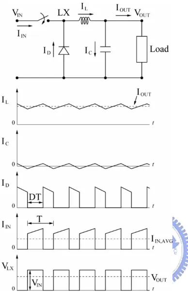
(43) Fig. 2.3. Buck converter topology and related waveforms.. For the buck converter of Fig. 2.3, the output voltage VOUT is less than the input voltage VIN, hence the name buck. When the switch is closed, input current flows through the filter inductor, the filter capacitor, and the load. When the switch is opened, the voltage across the inductor reverses since VL becomes a voltage source (VL = L × di/dt), and the energy stored in the inductor is delivered to the load. Since the current in the inductor cannot change instantaneously, the current flowing through the switch at the time the switch is opened now flows through the inductor, the capacitor, the load, and the diode. When the switch is again closed, the current, which was flowing through the diode, now flows through the switch and the cycle repeats. 19.
(44) The average output voltage is. VOUT = VIN × D. (2.1). Where D is the duty cycle. The duty cycle is the ratio of the switch on-time to the period T. Since. VIN × IIN = VOUT × IOUT. (2.2). The average input current is. IIN,AVG = IOUT × D. (2.3). We can see that when D = 100 %, VOUT = VIN and IOUT = IIN. Conversely, when the duty cycle approaches 0 %, the output voltage becomes very small and the peak input current becomes very large.. 2.2.2. Boost. For the boost converter of Fig. 2.4, the output voltage is greater than the input voltage, hence the name boost. With input voltage applied, the current flows through the inductor, the diode, the capacitor and the load. When the switch is closed, the current flows through the inductor and switch and in effect, the voltage across the inductor is the input voltage. When the switch is opened, the induced reverse voltage in the inductor is then in series-adding with the input voltage to increase the output voltage, and the current which was flowing through the switch now flows through the inductor, the diode, the capacitor, and the load. The energy stored in the inductor is transferred to the load. When the switch is again closed, the diode becomes reverse. 20.
(45) biased, the energy in the capacitor supplies the load voltage, and the cycle repeats.. Fig. 2.4. Boost converter topology and related waveforms.. The average output voltage is. (2.4). VOUT = VIN / (1-D). Where D is the duty cycle. The duty cycle is the ratio of the switch on-time to the period T. Since. VIN × IIN = VOUT × IOUT. (2.5) 21.
(46) The average input current is. (2.6). IIN,AVG = IOUT / (1-D). We can see that when D = 0 %, VOUT = VIN and IOUT = IIN. Conversely, when the duty cycle approaches 100 %, the output voltage does not necessarily approach infinity because the conducting operation of the semiconductor switch produces a peak current which will quickly exceed the safe operating area (SOA) limit. In other words, we can say that the conduction loss will limits the output voltage when D approaches 100 %.. 2.2.3. Buck-Boost. The buck-boost converter shown in Fig. 2.5 is referred to by many names. The buck-boost terminology will be used since the output voltage may be less than, or greater than, the input voltage. The converter is sometimes referred to as a flyback converter. The flyback designation is appropriate due to the inherent action of the inductor. This action in itself is sometimes referred to as a ringing-choke regulator. Also, the topology is sometimes referred to as an inverting regulator, since the output voltage polarity is opposite the input voltage polarity.. When the switch is closed, the current flows through the inductor since the diode is reverse biased. When the switch is opened, the current, which was flowing in the switch, now flows through the inductor, the diode, the capacitor and the load. The energy stored in the inductor is transferred to the load. When the switch is again closed, the current, which was flowing through the diode, now flows through the switch, and the diode becomes reverse biased.. 22.
(47) Fig. 2.5. Buck-boost converter topology and related waveforms.. The average output voltage is. -VOUT = VIN × D / (1-D). (2.7). Where D is the duty cycle. The duty cycle is the ratio of the switch on-time to the period T. Since. VIN × IIN = VOUT × IOUT. (2.8). The average input current is 23.
(48) IIN,AVG = IOUT × D / (1-D). (2.9). We can see that when D equals 50%, -VOUT = VIN and –IOUT = IIN.. 2.2.4. Synchronous Rectification. In the above topologies, we can see a master switch and a diode served as a slave switch. We can use a controlled switch (synchronous switch) instead of a diode in the above topologies, i.e. synchronous rectification. Synchronous rectification is used in DC-DC converters when low output voltage and high current is needed. Synchronous rectification utilizes power MOSFETs instead of rectifying diodes. These MOSFETs are synchronized to the converter frequency and perform more efficiently the rectification of the output voltage than rectifying diodes due to the low I × R drop through the channel. [40]-[41]. 2.3. MODULATION TECHNIQUES In this section, we briefly discuss about three modulation techniques.. 2.3.1. Fig. 2.6. Pulse Width Modulation (PWM). Switching signal of pulse width modulation (PWM). 24.
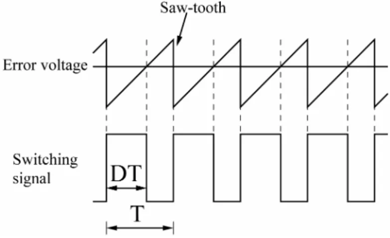
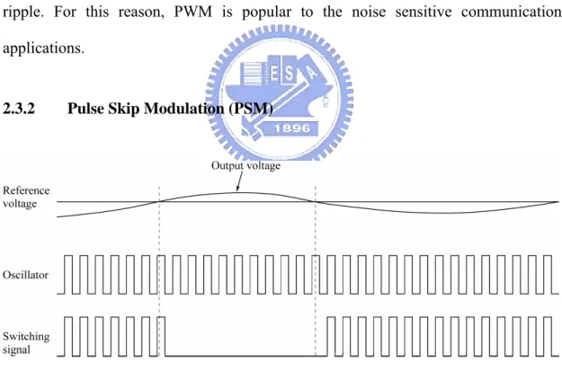
(49) The pulse width modulation (PWM) maintains a constant switching frequency and varies the duty ratio according to output voltage and load current. Take voltage mode control for example. The switching signal of PWM is shown in Fig. 2.6. The error voltage is modulated by a saw-tooth waveform generated by an oscillator. The switching frequency is determined by the oscillator and the pulse width is controlled by the voltage error. This modulation scheme provides high efficiency at medium to heavy load conditions. At light load condition, the reversed inductor current (may appear in synchronous rectification) and the switching losses degrade the efficiency. Because the switching frequency of PWM is fixed, the noise spectrum is relatively narrow. We can use simple low-pass filter to greatly reduce the peak-to-peak voltage ripple. For this reason, PWM is popular to the noise sensitive communication applications.. 2.3.2. Fig. 2.7. Pulse Skip Modulation (PSM). Output waveform and switching signal of pulse skip modulation (PSM).. A feature offered in many modern switching controllers is pulse skip modulation (PSM). Skip mode allows the regulator to skip cycles when they are not needed, which greatly improves efficiency at light loads. As shown in Fig. 2.7, in a PSM 25.
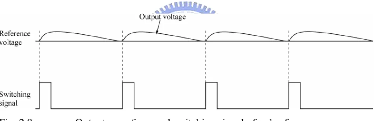
(50) system, there exists an oscillator as a timing reference. Each pulse of the switching signal starts with the clock signal. As long as the converter output is below the reference voltage, the PSM pulses continue to run the converter switch. Once the converter output reaches or exceeds the target, the PSM pulse is skipped. This operation will result in decreasing pulse density as the converter output reaches its target, or as the output loading decreases. When the converter output falls below the target, or as the output loading increases, the PSM pulse density will increase. However, the inductor selection is complicated, the peak-to-peak voltage ripple can be quite high, and the noise spectrum will vary greatly with the load.. 2.3.3. Fig. 2.8. Pulse Frequency Modulation (PFM). Output waveform and switching signal of pulse frequency modulation (PFM).. As shown in Fig. 2.8, pulse frequency modulation (PFM) is somewhat different from pulse skip modulation. They all reduce the pulse density in light load conditions and hence the efficiency can be boost under light load operation. The major difference of PFM to PSM is that the PFM does not need a clock signal. The pulse width is variable and the pulse repetition rate is varied in accordance with load current and input/output voltages. As soon as the output voltage reaches the bottom value of regulation, the main switch turns on until the inductor current reaches the peak current limit or until the predetermined time is up. The major drawback of PFM control is still 26.
(51) its varying switching frequency.. 2.4. PROTECTIONS OF SMPS In the design of a power supply it is prudent to provide protection circuitry to. protect against extreme and abnormal operating conditions that will inevitably occur when the supply is in use. These can occur in the form of output short circuits and excessive loads or high voltage transients on the input supply line. Many of the components in a power supply are handling powers greatly in excess of their dissipation capability. Under fault conditions it is quite possible that they may start to dissipate this power, leading to their rapid failure. The power supply designer has no control over these faults and therefore must incorporate circuitry to accommodate them safely. This falls into five broad categories: (1) over-current protection; (2) over-voltage protection; (3) inrush protection; (4) device protection; (5) over temperature protection. [4], [42]. 2.4.1. Over-Current Protection. In order to provide current limiting, some means of sensing over-current conditions must be provided. In an SMPS the commonest method of achieving current limiting is to control the switching activities of the switching transistors. Under fault conditions the transistors can be switched off. Cycle-by-cycle protection is a useful method of output current limiting in an SMPS.. The purpose of current limiting is two-fold: firstly to limit the dissipation in the power supply components to safe values and thereby prevent damage to them, and secondly to provide some protection to circuits and systems being powered by the 27.
(52) supply.. 2.4.2. Over-Voltage Protection. Over-voltage protection must deal with three possible situations: (1) reverse voltage on output; (2) external over-voltage on output; (3) internally generated over-voltage. The first two situations are reasonably easily dealt with by placing “catcher” diodes on the output. Fore reverse polarity protection, a normally reverse biased diode can be placed on the output. Normal over-voltage protection can be provided by a zener or avalanche diode whose voltage is in excess of the normal operating voltage of the power supply. Diodes for both types of protection must by amply rated to cope with the anticipated fault conditions.. It is important that a power supply does not give out an abnormally high voltage under fault conditions. If it did so it could easily damage the circuitry that it is powering. We can monitor the output voltage by an over-voltage control circuit. This is usually some form of comparator that is set to trigger under over-voltage conditions. Its output is used to stop the switching activity thereby shutting down the power supply; in much the same way as was done for cycle-by-cycle current limiting.. 2.4.3. Inrush Protection. In most SMPS designs it is desirable to introduce a certain delay during start-up, in order to avoid inrush current and output overshoots at turn-on. Circuits that are employed to perform this task are called soft-start circuits. In general they control the modulation circuitry to make the output to increase from zero to its operating value very “softly”.. 28.
(53) Fig. 2.9 shows how a soft-start circuit may be implemented in a PWM control circuit. At time t = 0, when the power supply is just turned on, capacitor C is discharged and the error amplifier output is held to ground through diode D1, thus inhibiting the comparator output.. Fig. 2.9. A typical soft-start circuit used in a PWM control circuit aids the gradual increase of the PWM signal to its operating value.. At time t = 0+, the capacitor starts to charge through resistor R with a time constant determined by τ = RC toward the charging voltage VSUPPLY. As capacitor C attains full charge, diode D1 is reverse biased, and therefore the output of the error amplifier is isolated from the soft-start network. The slow charge of capacitor C results in the gradual increase of the PWM waveform at the output of the comparator, and consequently a “soft start” of the switching element is initiated.. Diode D2 is used to bypass resistor R in order to discharge the capacitor C fast enough in case of system shutdown, thus initiating a new soft-start cycle even during very short interrupt periods. In some PWM control ICs, the resistor R has been substituted by an on-chip current generator, thus the only external element required to. 29.
(54) implement the soft-start feature is the addition of capacitor C.. 2.4.4. Device Protection. While dealing with protection it is probably worth mentioning voltage clamping. Here an avalanche diode is placed across the two conduction terminals of the power switch transistor. The breakdown voltage of the diode is chosen so that it is below the breakdown voltage of the power switch transistor and greater than the supply. In normal operation the diode will not conduct, but it will serve to clip any high voltage transients that might be harmful to the transistor.. 2.4.5. Over Temperature Protection. Although a power supply is protected by over-voltage and over-current protection circuits, it may undergo over heating condition because of high ambient temperature, improper heat sink design or malfunction of heat sink devices. The over temperature protection is needed to protect the power supply and all the devices and the circuits around the power supply under these conditions. Without over temperature protection, these abnormal conditions may cause fire and great damages.. The thermal sensors detect the temperature at the critical positions in the power supply. Once the temperature is higher than a preset safety margin, an over temperature signal will be issued to turn off the power switches. The heat energy will stop accumulation and the temperature may go down.. 2.5. PERFORMANCE SPECIFICATIONS While designing an electronic system, output voltage and current rating are 30.
(55) usually specified to the power supply. However, many other parameters are required to evaluate the performance of a power supply [4], [43]. In this section, some terms and definitions are described such that it will be easier to design or to evaluate a switching regulator.. 2.5.1. Efficiency. The efficiency of a power supply is defined as the ratio of the output power and the input power and is calculated as follows:. Efficiency =. POUT VOUT × I OUT = × 100% PIN VIN × I IN. (2.10). Efficiency can be regarded as the ratio of delivered power POUT to total consumed power PIN. Total power is the sum of the followings: (1) quiescent power: the quiescent current is the current flows into the chip. It is a goal of the chip designer to minimize this kind of power dissipation. (2) parasitic power: parasitic resistance in the output current path also dissipates power. (3) dynamic power: during the switching period, power is dissipated by charging/discharging gate capacitance of switching MOSFETs. It is a function of gate capacitance Cg, switching frequency fSW, and driving voltage VD. The relationship is Pd = Cg × Vdr2 × fSW. (4) output power: power delivered to the load. An efficient power supply should transfer as much input power to the output as possible. An inefficient regulator has two major disadvantages. First, energy is wasted. This is particularly important in a battery-powered system. Second, large heat sinks and good ventilation are required, which add to the size and weight of the regulator.. 2.5.2. Input Voltage Range 31.
(56) While delivering a regulated output voltage, a power converter must have the ability to operate under a wide input voltage range. Circuits in the power converter must keep constant operating characteristics under the input voltage variation. Sometimes the variation of input voltage can be several times to the minimum allowable input voltage. A closely related specification is line regulation, which will be discussed in section 2.5.4.. 2.5.3. Load Regulation. Output voltage regulation is a regulator’s ability to maintain its output voltage within the specified tolerance under various load disturbances. A measure of this ability is output impedance of the regulator. There is usually a feed back path in a regulator to compensate for such changes and keep the output close to the nominal value. Load regulation is the percentage change in the steady state output voltage when the load current changes from its minimum value to the fully rated current. Load regulation is defined as:. Load Regulation =. ΔVOUT / ΔV NOM × 100% ΔI LOAD. (2.11). Where VNOM is the nominal output voltage.. 2.5.4. Line Regulation. Similar to the definition of the load regulation, the line regulation is a measure of the effect of changes in the input voltage one the output voltage. The small signal line-to-output transfer function is called audio susceptibility. In some systems, input voltage may change as largely as 10 V. For example, in a notebook computer, the. 32.
(57) input voltage is 19 V provided by an AC adapter while it is around 8 V when battery power is used. There is a variety of methods used to specify line regulation. However, a common definition is:. Line Regulation =. ΔVOUT / ΔV NOM × 100% ΔV IN. (2.12). The specification of line regulation is usually given by %/V between maximum and minimum input voltages and at a specified loading condition.. 2.5.5. Transient Response. The transient response is a switching regulator’s response to sudden changes in load current or line voltage. It is measured by the magnitude of output voltage drop and the time of recovery. The transient response relates to the bandwidth of switching regulator, output capacitor, equivalent series resistance (ESR) of output capacitor and the load current.. A wide bandwidth regulator exhibits fast transient response. Limited by the bandwidth of switching frequency, switched mode regulators are slower than linear regulators. Loop crossover frequency is typically limited to 1/5 to 1/10 of the switching frequency. Therefore, a large output filter is required to compensate slow transient response. In order to reduce overshoot and ringing in output voltage, an adequate phase margin must be obtained. Control scheme also affects loop bandwidth, for example, the current-mode control provides faster response than the voltage mode.. If the output is suddenly switched from light load to full load, the shortage of the output current will cause a fall in output voltage. On the other hand, if the load is. 33.
(58) switched off, excess output current will cause a rise in the output voltage. The transient response is normally specified together with a recovery time and is stated as: V DEV × 100% V NOM. (2.13). Where VDEV is the maximum deviation from nominal output voltage VNOM at a full load transient. The transient recovery time was defined differently from 1% to 5% tolerance of the final settling value in different texts. We choose 1% tolerance to evaluate the performance of our work.. 2.5.6. Electromagnetic Interference (EMI). Electromagnetic interference (EMI) is a potential problem for the circuit designer. The switching process of a regulator produces voltage spikes resulting in EMI that interferes with proper operations of sensitive electronic equipments. The EMI spectrum begins at the switching frequency and often extends over 100 MHz that falls within the frequency bands commonly allocated for communications, such as low-frequency (LF), high-frequency (HF), and very-high frequency (VHF) bands. One obvious advantage of a fixed-frequency regulator is that the switching frequency and its harmonics are fixed which makes it easier to filter induced EMI.. There are two main EMI specifications that must be checked out, that for conducted noise and that for radiated noise. Usually if a design includes adequate screening and the conducted noise is kept under control, by means of appropriate filters, radiated noise is not too much of a problem.. 34.
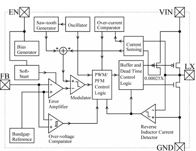
(59) CHAPTER 3 A MONOLITHIC CURRENT-MODE BUCK CONVERTER WITH ADVANCED CONTROL AND PROTECTION CIRCUITS 3.1. INTRODUCTION Portable battery-operated devices are more and more popular today. For these. devices, small size, light weight and long battery run-time are the main demands. The batteries had become a main portion in space and weight of these portable devices. As a result, enhancing the efficiency of power supply and management is very important to minimize the size and weight and to extend the battery run-time. The well-known power management strategy, sleep mode, shuts down the unused partial circuit to effectively reduce the power consumption [44]. Although sleep mode can save the power effectively in stand-by mode, there is no power saving in active mode because it operates with full current. The way of saving the power is to reduce the operating current but this usually reduces the circuit performance such as speed and noise immunity.. We focused on increasing the power efficiency and reducing die size without sacrificing high speed operation. Besides, safety operation is also an important consideration in power supply design. In this chapter, we propose the dynamic partial shutdown strategy (DPSS), current sensing, over-current protection, soft-start and PWM-PFM operation to achieve our goal. 35.
(60) The DPSS manages the power consumption at active mode to enhance the circuit performance per power consumption. Improvement was obvious, especially in lighter load with the PFM mode control [45].. Moreover, we modified the current sensing and slope compensation circuits in current-mode control [46]-[54] to simplify the design flows of various specifications. In current sensing circuit, a simple over-current protect comparator is developed. Its response speed is faster than the conventional comparator [53], [55]-[56]. But it consumes no additional quiescent power. With this circuit, the over-current protection, which is essential to voltage regulator, can be designed easily.. Most portable electronic devices have more than one power supply modules. Anyone of them may be shut down when the circuit supplied by it is unused. However, if we turn on the power supply module and don’t handle the load current demand from next stage properly, the inrush current demand to previous stage will result in impulse voltage drop and affect the circuit operation or shorten the life-time of batteries. On the other hand, inrush current can also cause the output to overshoot [57]. To overcome the induced effects, a soft-start time, usually 1 ~ 10 ms for portable electronic devices, is required at the beginning of the turn-on stage for voltage regulators. During soft-start time, the corresponding voltage regulator charges the output capacitor slowly, and then no inrush current is generated to affect the pre-stage circuit or to cause output overshoot. The conventional method of generating the soft-start time is costly in area [55], [58]-[59] or need the extra pin-out and discrete capacitor [57], [60]-[63]. This method results in increasing in cost, size and weight. This paper also presents a simple and area-effective circuit to generate soft-start time without the extra pin-out and the discrete capacitor. This circuit has the soft-start time. 36.
數據

+7

相關文件
一、訓練目標:充分了解在自動化 機械領域中應用 Arduino 控制,進 而能自行分析、設計與裝配各種控
(軟體應用) 根據商務活動之舉辦目標及系統需求,應用 Microsoft Office 文書處理 Word、電子試算表 Excel、電腦簡報 PowerPoint、資料庫 Access
在直流馬達控制系統中,為了減少流經馬達繞線電流及降低功率消耗等 目的,常常使用脈波寬度調變信號 (PWM)
※步進點主要應用於步進電路中。當不使 用步進指令時,步進點可作為一般的輔助 繼電器使用。 FX2 PLC的步進點可分為初
Moreover, when compared with the battery charger with the traditional pulse-width-modulated one, the novel battery charger with zero-current switching converter indeed reduces
Efficient Solution for More Driving Comfort and Safety, Robert
進而能自行分析、設計與裝配各 種控制電路,並能應用本班已符 合機電整合術科技能檢定的實習 設備進行實務上的實習。本課程 可習得習得氣壓-機構連結控制
木工程/都市設計與規劃/建築設備) 全日制,兼讀制 先進科技及管理學理學碩士 全日制,兼讀制 金融與精算數學理學碩士 全日制,兼讀制
