矽鍺與矽碳薄膜應用於金氧半場效電晶體和複晶矽鍺與多通道薄膜電晶體之研究
132
0
0
全文
(2) 矽鍺與矽碳薄膜應用於金氧半場效電晶體和 複晶矽鍺與多通道薄膜電晶體之研究 Study on SiGe and SiC Films in MOSFETs and Poly-SiGe and Multi-Channel Poly-Si in TFTs 研究生:謝明山. Student:Ming-Shan Shieh. 指導教授:雷添福 博士. Advisor:Dr. Tan-Fu Lei. 國立交通大學 電子工程學系 電子研究所 A Dissertation Submitted to Department of Electronics Engineering and Institute of Electronics College of Electrical and Computer Engineering National Chiao Tung University In Partial Fulfillment of the Requirements For the Degree of Doctor of Philosophy in Electronics Engineering May 2006 Hsinchu, Taiwan, Republic of China. 中華民國 九十五 年 五 月.
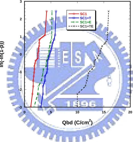
(3) 矽鍺與矽碳薄膜應用於金氧半場效電晶體和 複晶矽鍺與多通道薄膜電晶體之研究 學生: 謝 明 山. 指導教授: 雷 添 福 博士 國立交通大學. 電子工程學系 電子研究所博士班. 摘. 要. 本論文提出兩種元件,金氧半場效電晶體和複晶矽薄膜電晶體的製備來驗證 薄膜的效應和應用於元件上面的整合度。 首先,我們提出在矽鍺(Si0.8Ge0.2)磊晶薄膜中使用化學機械研磨方式來降低 晶格不匹配所造成粗糙的表面,我們將全面的研究研磨墊和研磨液對平坦度的影 響,接著使用一種新穎的研磨後清洗液應用於表面的清潔,經由加入表面清潔劑 (surfactant, TMAH)和螯合劑(chelating agent, EDTA)可以有效的去除表面的微粒 子和金屬殘留,表面的粗糙度也可有效的改善至 0.6 奈米。在電性方面,電容 的量測可以得到高的崩潰電壓、低的漏電流和較佳的累積崩潰電荷密度;在電晶 體的驗證上,可以得到十個百分比的電流增加。. I.
(4) 接著,探討使用矽碳(Si1-yCy, y=0.005)薄膜於動態臨限電壓電晶體(DTMOS) 的應用,經由此介面層引入通道可有效抑制硼原子的擴散,達成高的基底摻雜和 低的表面濃度分布。所形成的超陡峭(super-steep-retrograde)通道可使的表面散射 (surface scattering)現象降至最低,對於動態臨限電壓電晶體元件有較好轉導(1.2 倍)、高的導通電流(1.8 倍)和較低的臨限電壓(threshold voltage)表現,可以應用於 低電壓操作元件。 第二部分我們研究 n 型複晶矽薄膜電晶體在多重通道(multi-channel)的表 現。藉由增加通道的數目以提高閘極的控制能力,可以改善元件的電特性;包括 提高導通電流,降低臨界電壓及次臨限擺幅(subthreshold swing)。然而,元件的 可靠度卻會因此而變差。我們推測是由於在多重通道的結構中,靠近汲極端的電 場強度會增加,而導致更嚴重的碰撞游離(impact ionization)所造成。 在論文的最後,我們開發出一種改善複晶矽鍺薄膜電晶體(poly-SiGe TFTs) 的製程,經由氨氣的被覆(passivation)可以有效降低溫下矽鍺薄膜通道的缺陷; 而經過化學機械研磨對於表面平坦化處理可以有效減低表面的粗糙度,所形成複 晶矽鍺薄膜電晶體在結合此兩種處理的最佳化製程,可以得到很好的電性和可靠 度表現,達成應用在低溫製程薄膜電晶體的應用。. II.
(5) Study on SiGe and SiC Films in MOSFETs and Poly-SiGe and Multi-Channel Poly-Si in TFTs Student: Ming-Shan Shieh. Advisor: Dr. Tan-Fu Lei. Department of Electronics Engineering & Institute of Electronics National Chiao Tung University ABSTRACT In this thesis, two kinds of devices (MOSFETs and TFTs) have been fabricated to examine the films effect and integration of device characteristics. First, the effects of polish pad conditions and slurry solid contents on SiGe chemical mechanical polishing (CMP) process were investigated. The novel cleaning solutions with various surfactants and chelating agents for post-CMP SiGe were studied. By adding the surfactant (TMAH) and chelating agent (EDTA) into the diluted ammonium solution, removal efficiency of particles and metallic impurities is increased. The smooth strained-Si surface on flatten Si0.8Ge0.2 buffer layer of 0.6 nm can be achieved. The electrical performances of capacitors such as breakdown voltage, leakage current and Qbd are significantly improved for post-CMP cleaning. III.
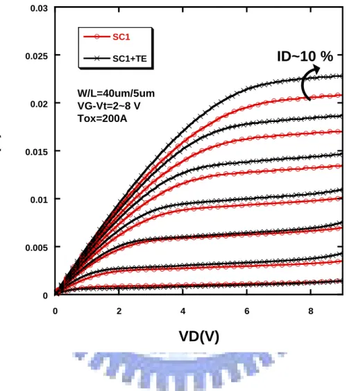
(6) Furthermore, the optimal condition of SC1+TE sample has increased about 10 % in drive current. This post-CMP cleaning process is useful for planarization of strain-relaxed SiGe virtual substrates in MOSFET application. Next, we have demonstrated the fabrication of Dynamic Threshold voltage MOSFET (DTMOS) using the Si1-yCy (y=0.005) incorporation inerlayer channel. Compare to conventional Si-DTMOS, the introduction of the Si1-yCy interlayer for this device is realized by super-steep-retrograde (SSR) channel profiles due to the retardation of boron diffusion. The excellent performances obtained in the Si1-yCy interlayer DTMOS are due to both the same substrate doping concentration and lower channel surface impurity concentration. So the surface impurity scattering could be reduces. We have successfully achieved the low threshold voltage and heavily doped substrate. DTMOS. with. superior. characteristics. in. terms. of. the. higher. transconductance (1.2×Gm) and saturation current (1.8×ID). It appears to be a very promising technology for nano-scale device and ultra-low voltage application. Then, we demonstrate the fabrication process and the electrical characteristics of n-channel polycrystalline silicon Thin-Film Transistors (poly-Si TFTs) with different numbers of channel stripes. The device’s electrical characteristics, such as on-current,. IV.
(7) threshold voltage, and subthreshold swing, were improved by increasing the number of channel stripes due to the enhancement of gate control. However, the electric field strength near the drain side was enlarged in multi-channel structures, causing severe impact ionization. Therefore, for the fabrication of highly reliable devices and to improve the yield of multi-channel TFTs, the channel structures must be carefully designed. Finally, the improvement of polycrystalline silicon germanium thin-film transistors (poly-SiGe TFTs) using NH3 passivation and CMP process was examined. Experimental results indicated that NH3 passivation could effectively improve the turn on characteristics. Moreover, the TFTs fabricated on polished poly-SiGe film exhibit higher carrier mobility, better subthreshold swing, lower threshold voltage, and higher on/off current ratio due to the smooth poly-SiGe interface. The results clearly show that by employing the plasma and CMP steps, significant improvement in the poly-SiGe TFTs with low thermal budget can be achieved.. V.
(8) 誌謝 首先我要向我的指導教授雷添福博士致上最高的敬意。感謝他在學業研究 與生活上給我的指導與鼓勵。在博士學習生涯中讓我學習到研究的態度及方 法。我也要感謝楊文祿教授為我打開半導體領域的基石,趙天生教授、簡昭欣 教授無論是在課堂上、研究上或平日會議時給我的非常多地指導與幫助,令我 獲益良多。另外和工研院蔡銘進組長以及陳邦旭博士的合作也獲得很大的助益 和幫忙。 感謝眾多的學長帶我進入半導體領域,李名鎮、李介文、張子云、俞正明學 長對我的照顧及協助。也感謝實驗室裡一起研究的夥伴,小強、建豪、楊紹明、 小賢、柏儀、獻德、志仰、家文,以及余俊、任逸、源俊、久盟、松霖、國誠、 伯浩、宗元、梓翔、俊嘉、統億、和錦石,有你們的陪伴與討論實驗過程不再枯 燥乏味而是充滿著歡樂。謝謝你們陪我度過漫長的實驗時間,讓我能以快樂的心 情面對實驗上與生活上的挑戰。 由衷地感激在實驗中曾給我幫助的朋友們,計測實驗室的彭作煌先生、教學 實驗室的彭兆光先生,與奈米中心的徐秀鑾、林素珠、黃月美、楊月嬌、范秀蘭、 陳悅婷、何惟梅、劉曉玲小姐以及奈米元件實驗室徐台鳳小姐、蔣秋芬小姐及其 他工程師們,若沒有你們的大力幫忙,我無法順利地完成此論文,在此獻上我最 深的敬意。 最後,謝謝我親愛的父親謝正平、母親陳素霞、姐姐謝竹君、姐夫陳旻閎、 芊芊、妹妹麗君與我可愛的女友葉玫君,感謝你們在我心情低落時給我打氣,在 我需要溫暖時給我照顧,謝謝你們陪我一路走過這漫長的求學生涯,僅此論文獻 給所有關心我的朋友。謝天~謝地~ 謝明山 謝謝大家!. VI.
(9) Contents Abstract (Chinese) ………………….……….………………………………………I Abstract (English). …………………………………………………….…………..III Acknowledge ……………………………………………………………………… VI Contents …………………………………………………………………………..VII Figure Captions & Table Lists.………………………..……………………......... X. Chapter 1 Introduction …………………………………………………………….1 1.1 Background .....………………………………………………………..……...1 1.2 Motivation …………….…………………..…………………………..……...3 1.3 Thesis Organization …………………….……………………………………..5 References …………………………………………………………………………8. Chapter 2 Deposition of SiGe and SiC Epitaxy Films by Ultra-High Vacuum Chemical Vapor Deposition (UHVCVD) System…....…....……………………...18 2.1 Introduction ……………….………….………………….……………...…..18 2.2 UHV-CVD System Features ….....……………...…...............………..……..22 2.3 Epitaxy film growth………………………………………………………….23 2.3.1 SiGe film ....…………………...…………………………………..…..23 2.3.2 SiC film..………………………………………….……………..……..23 2.4 CMP System Features……………………………………….…………….…24 2.5 Summary……..………………………………………………………………25 References ………………………..………………………………………………26. VII.
(10) Chapter 3 The CMP Process and Cleaning Solution for Planarization of Strain-Relaxed SiGe Virtual Substrates in MOSFET Application……………....33 3.1 Introduction …………………………………………………………………..33 3.2 Experimental …………………………………………………..……………..34 3.2.1 CMP procedure…………………………......……………...……….......34 3.2.2 Post CMP cleaning process……………….....……….……….............35 3.3 Results and Discussion ……………………………………………………….35 3.3.1 Material Analysis ………………………………………………………35 3.3.2 Device Characteristics…………………………......……….………......37 3.3.5 Device Reliability.……….……………………………………………..37 3.4 Summary ………………………………………………...…………………...38 References …………….………………………………………………………….39. Chapter 4. A Novel Dynamic Threshold Voltage MOSFET (DTMOS) Using. Heterostructure Channel of Si1-yCy Interlayer ..………………………………...56 4.1 Introduction …………………………………………………………………..56 4.2 Experimental …………………………………………………..……………..57 4.3 Results and Discussion ……………………………………………………….58 4.4 Summary ………………………………………………...…………………...59 References …………….………………………………………………………….61. Chapter 5. Electrical Characteristics and Reliability of Multi-channel. Polycrystalline Silicon Thin-Film Transistors…………………...…………...…...67 5.1 Introducion …………………….………………………………….…………67 5.2 Experimental …...……………………………………………….……………68 VIII.
(11) 5.3 Results and Discussion ………………………………………….…..……….69 5.3.1 Device characteristics ………………………………….………………69 5.3.2 Extraction of trap state density………………………………………..70 5.3.3 Device reliability ………………………………………………………71 5.4 Summary ...…………………………………………………………………...73 References ……..…………………………………………………………………74. Chapter 6 Effect of Chemical Mechanical Polish Process on Low-Temperature Poly-SiGe Thin-Film Transistors………………..………………………...…..….91 6.1 Introducion …………………………….……………………………………91 6.2 Experimental …...……………………………………………….…………..92 6.3 Results and Discussion..……………………………………………………93 6.3.1 Device characteristics …………………………………………………93 6.3.1 Extraction of density of state and reliability issues ……………………93 6.4 Summary ...…………………………………………………………………..94 References ……..…………………………………………………………………96. Chapter 7. Conclusions and Further Recommendations...……….…………...109. 7.1 Conclusions...………………………….……………………………………109 7.2 Further Recomendations..……………………………………….…………..111 Vita Publication list. IX.
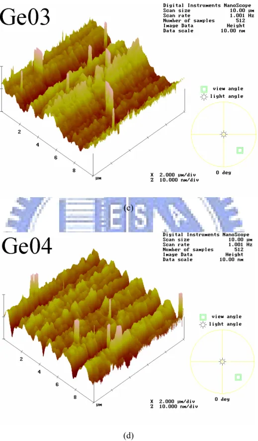
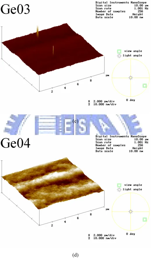
(12) Figure Captions Chapter 2 Fig. 2.1 Epitaxial films growth system SIRIUS (a) façade of the system and (b) process chamber. Fig. 2.2 Configurations of vertical SiGe epitaxial growth system. Fig. 2.3 Configurations of film growth system inside layout around process chamber.. Chapter 3 Fig. 3.1 AFM images of strained-relaxed SiGe buffer layers before CMP process. Different slurry and pad conditions for (a)Ge01, (b)Ge02, (c)Ge03 and (d)Ge04 samples. Fig. 3.2 AFM images of strained-relaxed SiGe buffer layers after CMP process. Different slurry and pad conditions for (a)Ge01, (b)Ge02, (c)Ge03 and (d)Ge04 samples. Fig. 3.3 Removal rate of (a) time dependent and (b) pressure dependent in SiGe layers. X.
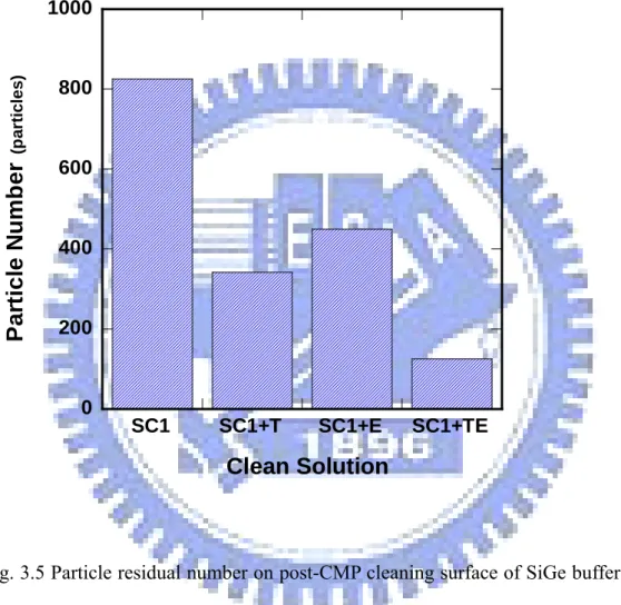
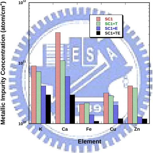
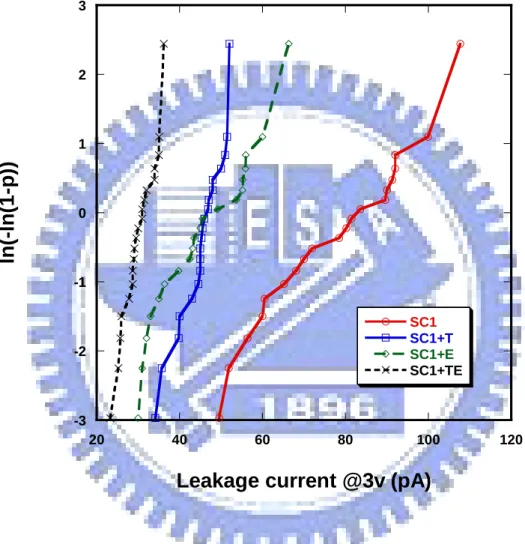
(13) Fig. 3.4 AFM images of strained-Si surfaces without and with CMP process. The RMS values are (a) without CMP 1.8 nm and (b) with CMP process 0.6 nm respectively. Fig. 3.5 Particle residual number on post-CMP cleaning surface of SiGe buffer layers in different solutions. Fig. 3.6 The metallic contaminant concentration on SiGe buffer layer by TXRF. Fig. 3.7 The current vs. voltage characteristic of MOS capacitors with 20 nm TEOS oxide on the strained-Si with different cleaning method. Fig. 3.8 The cumulative distribution of leakage current of MOS capacitors with different cleaning method. Fig. 3.9 Distribution of breakdown voltage distribution of MOS capacitors. Fig. 3.10 The charge-to-breakdown of MOS capacitors under constant current stress in four kinds of different solutions. Fig. 3.11 The current enhancement of 10 % between SC1 and SC1+TE samples.. Chapter 4 Fig. 4.1 SIMS measurements of boron and carbon diffusion profile in the channel. XI.
(14) region. Fig. 4.2 Threshold voltage versus different body bias for a W/L=10μm/5μm. NMOSFET. Fig. 4.3 Subthreshold characteristics of NMOSFET under standard-mode and DT-mode. Drain current and transconductance (Gm) for the samples with and without Si1-yCy layer. Fig. 4.4 Drain current of (a) without Si1-yCy , and (b) with Si1-yCy devices in standard-mode and DT-mode. Gate voltage varies from 0.2 to 0.7 V in 0.1 V step.. Chapter 5 Fig. 5.1 Process flow of conventional and multi-channel poly-Si TFTs. Fig. 5.2 The cross-section of conventional and multi-channel poly-Si TFTs is parallel to the direction of the source and drain electrodes. Fig. 5.3 The cross-section of conventional and multi-channel poly-Si TFTs is perpendicular to the direction of the source and drain electrode. Fig. 5.4 Top view of (a) the conventional and (b) multi-channel poly-Si TFTs. The. XII.
(15) effective channel width Weff = 40μm ; channel length L = 2μm. Fig. 5.5 Transfer characteristics of the conventional and the proposed multi-channel poly-Si TFTs with different stripes of channel Fig. 5.6 Field effect mobility of conventional and proposed multi-channel poly-Si TFTs with different number of stripes in the channel. Fig. 5.7 Trap state density of conventional and proposed multi-channel poly-Si TFTs with different number of stripes in the channel. Fig. 5.8 Increasing ratio of the effective channel width and the on-state current as a function of number of channel stripes. Fig. 5.9 Output characteristics of conventional and proposed poly-Si TFTs with different numbers of stripes in the channel. (VG – Vth = 0.5; 2; 3.5V). Fig. 5.10 (a) On-state current, (b) field effect mobility, and (c) threshold voltage as a function of different gate lengths with the number of channel stripes. Fig. 5.11 (a) On-current, and (b) threshold voltage degradation as a function of time under hot-carrier stress. Fig. 5.12 Trap state density (Nt), before and after 4 s, 10 s, and 100 s stress with different numbers of channel stripes.. XIII.
(16) Fig. 5.13 Increasing ratio of trap state density after 4 s, 10 s, and 100 s stress with different numbers of channel stripes. Chapter 6 Fig. 6.1 Process flow for SiGe TFTs. Fig. 6.2 Three-dimensional AFM images of SiGe film surface (a)before CMP process, and after CMP polishing process for (b)10 seconds and(c)20 seconds, respectively. Fig. 6.3 Transfer curves of unpolished TFTs with various NH3 plasma treatment times in 30, 60, 120 minutes. Fig. 6.4 Transfer curves of SiGe TFTs with and without CMP polishing process. Fig. 6.5 Density of states in band gap of the device using the polished SiGe film as channel with different NH3 plasma treatment times. Fig. 6.6 Threshold voltage degradation as a function of stress time under hot-carrier stress.. XIV.
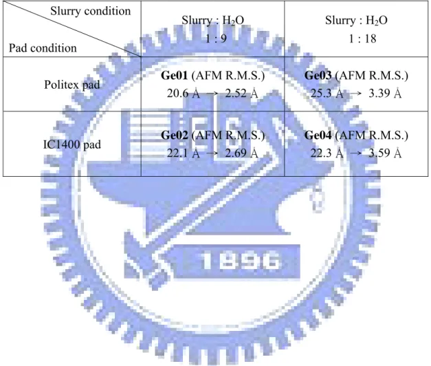
(17) Table Lists Chapter 3 Table 3.1 Different slurry and pad conditions for Ge01, Ge02, Ge03 and Ge04 samples.. Chapter 5 Table 5.1 Summary of device parameters of conventional and proposed multi-channel poly-Si TFTs (W/L = 40μm/2μm) with different numbers of stripes in the. channel.. Chapter 6 Table 6.1 Parameters of CMP process condition. Table 6.2 Characteristics of TFTs with and without CMP process.. XV.
(18) Chapter 1 Introduction 1.1 Background The past several years have witnessed rapid growth in the study of strained silicon due to its potential ability to improve the performance of very large scale integrated (VLSI) circuits independent of geometric scaling. Historically, performance improvements in metal-oxide semiconductor field-effect transistors (MOSFETs) have been attained by shrinking device dimensions such as the gate length and gate oxide thickness. However, the practical benefit of scaling is declining as physical and economic limits are approached, and novel solutions are increasingly being sought. The incorporation of new materials, from the interconnect level (Cu, low-k), to the gate stack (high-k dielectrics, metal gate electrodes), and even the substrate [strained-Si, silicon-on-insulator (SOI) wafers] is emerging as an important way to continue to improve circuit performance. Strain improves MOSFET drive currents by fundamentally altering the band structure of the channel and can therefore enhance performance even at aggressively scaled channel lengths. There has been significant interest in SiGe heteroepitaxial growth on silicon substrates, because Si/ SiGe hetero-structures allow band-gap engineering to be used in conjunction with silicon technology. Of particular interest are the pseudomorphic p-type Si1−xGex channel (x =10-20%) modulation doped field effect transistor (MODFET), the n-type strained Si channel MODFET and the p-type strained Si1−xGex channel MODFET (x > 70%). Excellent review articles on these high mobility devices can be found in [1]-[5].. 1.
(19) Strained silicon on relaxed silicon-germanium (SiGe) substrates is a promising candidate for transistor performance enhancement [6]. Strain splits the degeneracy in the conduction and valence bands of Si, enhances the transport properties of electrons and holes, and provides transistor speed enhancement. High quality strained-relaxed buffer layers are required for the high performance devices. But the relaxed SiGe layers tend to have the threading dislocation and rough surface. Several methods such as the graded buffer layers [7] and low temperature buffer [8] methods have been studies. The relaxation during the growth of the visual substrate results in a cross-hatch (misfit dislocations) which increases the surface roughness. Next, we introduce the overview of poly-Si thin-film transistor. The TFTs have been widely investigated in industrial applications, such as active-matrix liquid-crystal displays (AMLCDs), high density static random access memories (SRAMs), electrical erasable programming read only memories (EEPROM) and candidate for 3-D ICs’ applications, etc. Within those applications, the application of AMLCDs is the major driving force to promote the developments of poly-Si TFT technology [9]-[17]. It has been reported that the α-Si films can be crystallized by several techniques, such as SPC (solid-phase crystallization) [18], [19]; ELA (excimer laser annealing) [20], [21] and MILC (metal-induced lateral crystallization) [22] to obtain a large grain size of poly-Si to raise the field effect mobility. Additionally, there were other methods such as plasma treatments to passivate the defects in the channel or narrowing the channel width to reduce the trap state density. The electrical characteristics of poly-Si TFT is mainly influenced by the defects in the grain boundaries and within the grain [23]. Trap states resulted from those defects within the channel lead to poor device performance, such as low field effect mobility, large leakage current [24], bad subthreshold slope and high threshold voltage. It is. 2.
(20) necessary to recover the trap states in the poly-Si channel to enhance the device performance. For this purpose, hydrogenation has been suggested to be an effective method [25]-[27]. The atomic hydrogen can recover interface states between poly-Si and SiO2 and passivate defects in the grain boundaries to improve the device characteristics. Furthermore, other different treatments have been demonstrated to further enhance the device performance, for instance, H2/N2 mixture plasma [28], nitrogen implantation with H2 plasma [29], pre-oxidation NH3 annealing with H2 plasma [30], NH3 plasma [31], O2 plasma [32], and H2/O2 plasma [33]. The atomic nitrogen and oxygen also have passivation effect by themselves and moreover the hydrogen passivation effects are greatly enhanced with their incorporation, leading to the observed great improvement in the device performance. Nevertheless, poly-Si TFTs with hydrogenation treatment have a troublesome problem in the performance degradation for the devices under electrical stress. It have been reported that the reliability of hydrogen-passivated TFTs was considerably poor because weak Si-H bonds or Si-Si bonds might be broken to cause the creation of trap states in the poly-Si channel [34].. 1.2 Motivation The epitaxy films used in chapter 3 and 4 were prepared by the UHVCVD system. First, the chemical mechanical polishing (CMP) process has become the mainstream of globe planarization technique in fabrication of deep submicron integrated circuit. To reduce this surface roughness, the CMP process is applied to the grown layers to reduce the surface roughness. Some previous works have been introduced it into polishing SiGe buffer layers [35]-[41]. The high crystalline quality of the re-growth layer with smooth interface makes it possible to fabricate high. 3.
(21) performance SiGe device with low surface roughness scattering. However, the wafer surface after CMP process is seriously contaminated with particles and metallic impurities form polishing slurry. In addition, the metallic impurities will induce many crystal defects in Si wafer during thermal process [42]. And the planarized SiGe buffer layer roughness will be increased due to the etching effect [43]. Our previous studies have found that the novel post-CMP cleaning solution can significantly reduce the contamination retention [44]-[46]. We applied it to the post-CMP cleaning on SiGe buffer layer. Furthermore, the capacitor and MOSFET electrical characteristics of strained-Si re-growth on various solutions process were also evaluated.. Next, the epitaxy Si1-yCy films also applied to the novel device application. A n-channel DTMOS with boron implantation was studied [47], [48]. The Dynamic Threshold MOSFET (DTMOS) structure offers a promising technology to achieve both high speed and low power performance. In order to take full advantage of the high current drive inherent in DTMOS, Chang et al. proposed the use of super-steep-retrograde (SSR) indium-channel profile [49], [50]. On the other hand, Takagi et al. also proposed a novel SiGe channel heterostructure DTMOS for reducing the threshold voltage in spite of keeping impurity doping level at the body region [51]. Transient enhanced diffusion (TED) of boron and phosphorus during annealing of implantation damage can be suppressed by incorporation of substitutional carbon. Si1-yCy layer have been applied to suppress boron diffusion in hetero-junction bipolar transistors (HBT). The incorporation of substitutional carbon in silicon can reduce fast diffusion spices of boron diffusion in silicon [52]-[57]. An explanation for this behavior has been provided that the substitutional carbon present in the silicon substrate acts as the sink for silicon self-interstitial and the carbon spices are displaced by the silicon self-interstitial during thermal treatment processes. We 4.
(22) will examine the DTMOS device with the interlayer SiC films.. Moreover, the gate electrode across the channel may induce side-channels in both sides of the channel region, and these side-channels may increase the effective channel width. Especially when the channel width is scaled down, the side-channel effect is more distinct. The average carrier concentration in the channel region of the corner of the poly-Si gate electrode is increased by electrostatic focusing from the top gate and both side gates of the stripes [58]. It is believed that the gate control capability was obviously improved in narrow width devices. Accordingly, poly-Si TFTs with narrow and multiple channels have been proposed to enhance electrical characteristics [59]-[61]. However, no complete reliability analysis has been carried out in the poly-Si TFTs with narrow and multiple channels. We will demonstrate the fabrication process and the electrical reliability of n-channel poly-Si TFTs with different channel stripes.. Finally, silicon germanium (SiGe) is a promising candidate for use as the TFTs channel film, as it requires lower processing temperature than Si. Since the melting point of SiGe is lower than that of Si, the lower process temperature can be used for TFTs fabrication [62]-[65]. For low-temperature solid phase crystallization (LT-SPC) applications, SiGe is particularly advantageous, as it requires substantially shorter annealing cycles than required for the crystallization of Si. To date, using conventional SPC processing with no pre-amorphization implant, SiGe TFTs performance has generally been worse than poly-Si TFT performance. The SiGe TFTs performance has been improved substantially through the use of thin Si interlayer to improve the gate oxide interface [66]. However, little has been done to improve the intrinsic quality of the SiGe channel film itself; the binary nature of the SiGe system. 5.
(23) complicates optimization and modeling substantially. In previously described preliminary optimization of SiGe TFTs through the use of multi-factorial design of experiment techniques [67], [68]. However, the rough surface of channel causes the poor performance and the low reliability of the device. It is shown that a planarized polysilicon surface will yield TFTs with improved performance and reliability. The CMP process has been used extensively for smoothing surface of polysilicon films [69]-[74]. Thus it is possible to be applied to smooth the poly-SiGe films. In this study, we develop optimization strategies for fabrication of high-performance SiGe TFTs.. 1.3 Thesis Organization There are six chapters in this dissertation. This thesis is organized as follow: In chapter 1, the overview of our study and motivations of this thesis are described. In chapter 2, the introduction of the UHVCVD system instrument used in our experiments. We have fabricated high-quality relaxed SiGe films using an intermediate Si interlayer within the channel region and SiC films. In chapter 3, we have investigated planarization of rough surfaces of strain-relaxed Si0.8Ge0.2 buffer layer by CMP and post-CMP cleaning. The effects of polish pad conditions and slurry solid contents on SiGe CMP process were investigated. By optimizing the polishing conditions, the smooth strained-Si surface on flatten Si0.8Ge0.2 buffer layer of 0.6 nm can be achieved. The novel cleaning solutions with various surfactants and chelating agents for post-CMP SiGe were studied. The surfactant (TMAH) and chelating agent (EDTA) into the diluted ammonium solution, removal efficiency of particles and metallic impurities is increased.. 6.
(24) In chapter 4, we have demonstrated the fabrication of Dynamic Threshold voltage MOSFET (DTMOS) using the Si1-yCy (y=0.005) incorporation interlayer channel. Compare to conventional Si-DTMOS, the introduction of the Si1-yCy interlayer for this device is realized by super-steep-retrograde (SSR) channel profiles due to the retardation of boron diffusion. A low surface channel impurity with heavily doped substrate can be achieved simultaneously. We have developed a novel n-channel Si1-yCy interlayer heterostructure DTMOS structure. In chapter 5, we demonstrate the fabrication process and the electrical characteristics of n-channel polycrystalline silicon Thin-Film Transistors with different numbers of channel stripes. Poly-Si TFTs with multiple channels have better performance than conventional TFTs. Then, we fully discuss about the reliability of poly-Si TFTs with multiple channels. The effects of the number of channel stripes in multi-channel TFTs on performance and reliability have been investigated. For the fabrication of highly reliable devices and to improve the yield of multi-channel TFTs, the channel structures must be carefully designed. In chapter 6, the improvement of polycrystalline silicon germanium thin-film transistors (poly-SiGe TFTs) using NH3 passivation and chemical mechanical polishing (CMP) process was examined. Experimental results indicated that NH3 passivation could effectively improve the turn on characteristics. Finally, conclusions of this dissertation and recommendation for further research are presented in chapter 7. The compatibility of the propose technology can meet the trend of process requirement. It is expected that the processes in this thesis can be good choices in the future deep-submicron generation.. 7.
(25) References: [1] F. Schäffler, “High-mobility Si and Ge structures,” Semicond. Sci. Technol., vol. 12, pp. 1515-1549, 1997. [2] T. E. Whall and E. H. C. Parker, “SiGe heterostructures for FET applications,” J. Phys. D: Appl. Phys., vol. 31, pp. 1397-1416, 1998. [3] U. König, M. Glück and G. Höck, “Si/ SiGe field-effect transistors,” J. Vac. Sci. Technol. B, vol. 16, no. 5, pp. 2609-2614, 1998. [4] C. K. Maiti, L. K. Bera and S. Chattopadhya, “Strained-Si heterostructure field effect transistors,” Semicond. Sci. Technol., vol. 13, pp. 1225-1246, 1998. [5] D. J. Paul, “Silicon germanium heterostructures in electronics: the present and the future,” Thin Solid Films, vol. 321, no. 1-2, pp. 172-180, 1998. [6] J. L. Hoyt, H. M. Nayfeh, S. Eguchi, I. Aberg, G. Xia, T. Drake, E. A. Fitzgerald and D. A. Antoniadis, “Strained silicon MOSFET technology,”in IEDM Tech. Dig., 2002, pp. 22-26. [7] P. M. Mooney, J. L. Jordan-Sweet, K. Ismail, J. O. Chu, R. M. Feestra, and F. K. LeGoues, “Relaxed Si0.7Ge0.3 buffer layers for high-mobility devices,” Appl. Phys. Lett., vol. 67, no.16, pp. 2373-2375, 1995. [8] T. Ueno, T. Irisawa, Y. Shiraki, A. Uedono and S. Tanigawa, “Low temperature buffer growth for modulation doped SiGe/Ge/SiGe heterostructures with high hole mobility,” Thin Solid Films, vol. 369, pp. 320-323, 2000. [9] C. H. Fa, and T. T. Jew, “The polysilicon insulated-gate field-effect transistor,” IEEE Trans. Electron Devices, vol. 13, no. 2, pp. 290, 1966. [10] Y. Oana, “Current and future technology of low-temperature poly-Si TFT-LCDs,” Journal of the SID, vol. 9, pp. 169-172, 2001. [11] S. Morozumi, K. Oguchi, S. Yazawa, Y. Kodaira, H. Ohshima, and T. Mano,. 8.
(26) “B/W and color LC video display addressed by poly-Si TFTs,” SID Dig., pp.156, 1983. [12] R. E. Proano, R. S. Misage, D. Jones, and D. G. Ast, “Guest-host active matrix liquid-crystal display using high-voltage polysilicon thin film transistors,” IEEE Trans. Electron Devices, vol. 38, pp. 1781, 1991. [13] S. Batra, “Development of drain-offset (DO) TFT technology for high density SRAM’s,” Extended Abstracts, vol.94-2, in Electrochemical Soc. Fall Mtg., Miami Beach, FL, Oct. pp. 677,1994. [14] M. Cao, et al., “A simple EEPROM cell using twin polysilicon thin-film transistors,” IEEE Trans. Electron Devices, vol. 15, pp. 304, 1994. [15] N. D. Young, G. Harkin, R. M. Bunn, D. J. McCulloch, and I. D. French, “The fabrication and characterization of EEPROM arrays on glass using a low temperature poly-Si TFT process,” IEEE Trans. Electron Devices, vol. 43, pp. 1930, 1995. [16] K. Banerjee, S. J. Souri, P. Kapur, and K. C. Saraswat, “3-D ICs: a novel chip design for improving deep-submicrometer interconnect performance and system-on-chip integration,” Proceedings of the IEEE, vol.89, pp. 602-633, 2001. [17] W. G. Hawkins, “Polycrystalline-silicon device technology for large-area electronics,” IEEE Trans. Electron Devices, vol. 33, pp. 477-481, 1986. [18] H. Kuriyama et al., “Enlargement of poly-Si film grain size by excimer laser annealing and its application to high-performance poly-Si thin film transistor,” Jpn. J. Appl. Phys., vol. 30, pp. 3700-3703, 1991. [19] A. Nakamura, F. Emoto, E. Fujii, and A. Tamamoto, “A high-reliability, low-operation-voltage monolithic active-matrix LCD by using advanced solid-phase growth technique,” IEDM Tech. pp.847, 1990. [20] G. K. Guist, and T. W. Sigmon, “High-performance laser-processed polysilicon 9.
(27) thin-film transistors,” IEEE Electron Device Lett., vol. 20, no. 2, pp. 77-79, Feb. 1999. [21] N. Kudo, N. Kusumoto, T. Inushima, and S. Yamazaki, “Characterization of polycrystalline-Si thin-film transistors fabricated by excimer laser annealing method,” IEEE Trans. Electron Devices, vol. 40, pp. 1876-1879, Oct. 1994. [22] S. W. Lee, T. H. Ihn, and S. K. Joo, “Fabrication of high-mobility p-channel poly-Si thin-film transistors by self-aligned metal-induced lateral crystallization,” IEEE Electron Device Lett., vol. 17, no. 8, pp. 407-409, Aug. 1996. [23] I. W. Wu, W. B. Jackson, T. Y. Huang, A. G. Lewis, and A. Ciang, “Passivation kinetics of two types of defeats in polysilicon TFT by plasma hydrogenation,” IEEE Electron Devices lett., vol. 12, pp. 181-183, 1991. [24] J. G. Fossum, A. Ortiz-Conde, H. Shicjijo, abd S. K. Banerjee, “Anomalous leakage current in LPCVD polysilicon MOSFET’s,” IEEE Trans. Electron Devices, vol. 32, pp. 1878-1882, 1985. [25] A. Mimura, N. Konishi, K. Ono, J-I. Ohwada, Y. Hosokawa, Y. A. Ono, Y. Suzuki, K. Miyata, and H. Kawakami, “High performance low-temperature poly-Si n-channel TFT’s for LCD,” IEEE Trans. Electron Devices, vol. 32, pp. 351-359, 1989. [26] K. Baert, H. Murai, K. Kobayashi, H. Namizaki, and M. Nunoshita, “Hydragen passivation of polysilicon thin-film-transistors by electron-cyclotron-resonance plasma,” Jpn. J. Appl. Phys., vol. 32, pp. 2601-2606, 1993. [27] A. Yin, and S. J. Fonash, “High-performance p-channel poly-Si TFT’s using electron cyclotron resonance hydrogen plasma passivation,” IEEE Electron Devices lett., vol. 15, no. 12, pp. 502-503, 1994. [28] M. J. Tasi, F. S. Wang, K. L. Cheng, S. Y. Wang, M. S. Feng, and H. C. Chen, “Characterization of H2/N2 plasma passivation process for poly-Si thin-film 10.
(28) transistors (TFTs),” Solid State Electronics, vol. 38, no. 5, pp.1233-1238, 1995 [29] C. K. Yang, T. F. Lei, C. L. Lee, “Improved electrical characteristics of thin-film transistors fabricated on nitrogen-implanted Polysilicon films,” IEDM Tech Dig., pp. 505, 1994. [30] C. K. Yang, T. F. Lei, C. L. Lee, “The combined effects of low pressure NH3 annealing and H2 plasma hydrogenation on polysilicon thin-film-transistors,” IEEE Electron Devices lett., vol. 15, pp. 389-390, 1994. [31] H. C. Cheng, F. S. Wang, and C. Y. Huang, “Effects of NH3 plasma passivation on n-channel Polycrystalline silicon thin-film-transistors,” IEEE Trans. Electron Devices, vol. 44, no. 1, pp. 64-68, 1997. [32] S. Ikeda, S. Hashiba, I. Kuramoto, H. Katoh, S. Ariga, T. Yamanka, T. Hashimoto, N. Hashimoto, and S. Megura, “A polysilicon transistor technology for large capacitance SRAMS,” in IEDM Tech. Dig., pp. 459-463, 1990. [33] H. N. Chern, C. L. Lee, and T. F. Lei, “H2/O2 plasma on polysilicon thin film transistor,” IEEE Electron Device Lett., vol. 14, pp.115-117, 1993. [34] I. W. Wu, W. B. Jackson, T. Y. Huang, A. G. Lewis, and A. Chiang, “Mechanism of device degradation in n- and p-channel polysilicon TFT’s by electrical stressing,” IEEE Electron Devices lett., vol. 11, pp. 167-170, 1990. [35] K. Sawano, K. Kawaguchi, T. Ueno, S. Koh, K. Nakagawa and Y. Shiraki, “Surface smoothing of SiGe strain-relaxed buffer layers by chemical mechanical polishing,” Mater. Sci. Eng. B, vol. 89, no.1-3, pp. 406-409, 2002. [36] K. Sawano, K. Arimoto,Y. Hirose, S. Koh, N. Usami , K. Nakagawa, T. Hattori , and Y. Shiraki, “Planarization of SiGe virtual substrates by CMP and its application to strained Si modulation-doped structures,” J. Cryst. Growth, vol. 251, no.1-4, pp. 693-696, 2003. [37] K. Sawano, K. Arimoto, Y. Hirose, S. Koh, N. Usami, K. Nakagawa, I. Hattori, Y. 11.
(29) Shiraki, “Planarization of SiGe virtual substrates by CMP and its application to strained Si modulation-doped structures,” in Conf. Molecular Beam Epitaxy, 2002, pp. 15-20.2002. [38] N. Sugii, D. Hisamoto, K. Washio, N. Yokoyama and S. Kimura, “Enhanced performance of strained Strained-Si MOSFETs on CMP SiGe virtual substrate,” in IEDM Tech. Dig., 2001, pp. 33.4.1-33.4.4. [39] K. Sawano, S. Koh, Y. Shiraki, Y. Hirose, T. Hattori, and K. Nakagawa, “Mobility enhancement in strained Si modulation-doped structures by chemical mechanical polishing,” Appl. Phys. Lett., vol. 82, pp. 412-415, 2003. [40] N. Sugii, D. Hisamoto, K. Washio, N. Yokoyama and S. Kimura, “Performance enhancement of strained-Si MOSFETs fabricated on a chemical-mechanicalpolished SiGe substrate,” IEEE Trans. Electron Devices, vol. 49, no. 12, pp. 223-2243, 2002. [41] M. T, Currie, C. W. Leitz, T. A. Langdo, G. Taraschi, E. A. Fitzgerald and D. A. Antoniadis, “Carrier mobilities and process stability of strained Si n- and p-MOSFETs on SiGe virtual substrates,” J. Vac. Sci. Technol. B, vol.19, no. 6, pp. 2268-2279, 2001. [42] N. Miyashita, M. Shimomura, Y. Minami, I. Katakabe, H. Nojo, H. Ohashi and M. Abe, “A new post CMP cleaning method for trench isolation process,” ISMIC’96, 1996, p.161. [43] K. Sawano, K. Kawaguchi, S. Koh, Y. Hirose, T. Hattori, K. Nakagawa and Y. Shiraki, “Surface Planarization of Strain-Relaxed SiGe Buffer Layers by CMP and Post Cleaning,”J. Electrochem. Soc., vol. 150, pp. G376-G379, 2003. [44] T. P. Pan, T. F. Lei, T. S. Chao, M. C. Liaw, F. H. Ko and C. P. Lu, “One-step cleaning solution to replace the conventional RCA two-step cleaning recipe for pre-gate oxide cleaning,” J. Electrochem. Soc., vol. 148, pp. G315-G319, 2001. 12.
(30) [45] T. M. Pan, T. F. Lei, C. C. Chen, T. S. Chao, M. C. Liaw, W. L. Yang, M. S. Tsai, C. P. Lu, W. H. Chang, “Novel cleaning solutions for polysilicon film post chemical mechanical polishing,” IEEE Electron Device Lett., vol. 21, no. 7, pp. 338-340, 2003. [46] T. M. Pan, T. F. Lei, F. H. Ko, T. S. Chao, T. H. Chiu, Y. H. Lee, C. P. Lu, “Comparison of novel cleaning solutions with various chelating agents for post-CMP cleaning on poly-Si film,” IEEE Trans. Semiconductor Manufacturing, vol. 14, no. 4, pp. 365-371, 2001. [47] F. Assaderaghi, D. Sinitsky, S. Paske, J. Boker, P. K. Ko, and C. Hu, “A dynamic threshold voltage (DTMOS) for ultra-low voltage operation,” in IEDM Tech. Dig., Dec. 1994, pp. 809–812. [48] F. Assaderaghi, D. Sinitsky, S. Parke, J. Bokor, P. K. Ko, C. Hu,” Dynamic threshold-voltage MOSFET (DTMOS) for ultra-low voltage VLSI,” IEEE Trans. Electron Devices, vol. 44, pp. 414–422, Mar. 1997. [49] S. J. Chang, C. Y. Chang, C. Chen, T. S. Chao, Y. J. Lee,and T. Y. Huang,” High-performance and high-reliability 80-nm gate-length DTMOS with indium super steep retrograde channel,” IEEE Trans. Electron Devices, vol. 47, pp. 2379–2384, Dec. 2000. [50] S. J. Chang, C. Y. Chang, T. S. Chao, and T. Y. Huang,” High performance 0.1 µm dynamic threshold MOSFET using indium channel implantation,” Electron Device Lett., vol.21, pp. 127–129, Mar. 2000.. 13. IEEE.
(31) [51] T. Takagi, A. Inoue, Y. Hara, Y. Kanzawa, and M. Kubo, “A novel high performance SiGe channel heterostructure dynamic threshold pMOSFET (HDTMOS),” IEEE Electron Device Lett., vol.22, pp. 206–208, May 2001. [52] P. A. Stolk, D. J. Eaglesham, H.-J. Gossmann, and J. M. Poate, “Carbon incorporation in silicon for suppressing interstitial-enhanced boron diffusion,” Appl. Phys. Lett., vol. 66, pp. 1370–1372, Mar. 1995. [53] H. Rucker, B. Heinemann, W. Ropke, R. Kurps, D. Kruger, G. Lippert, and H. J. Osten, “Suppressed diffusion of boron and carbon in carbon-rich silicon,” Appl. Phys. Lett., vol. 73, pp. 1682–1684, Sep. 1998. [54] H. Rucker, B. Heinemann, D. Bolze, R. Kurps, D. Kruger, G. Lippert, and H. J. Osten, “The impact of supersaturated carbon on transient enhanced diffusion,” Appl. Phys. Lett., vol. 74, pp. 3377–3379, May 1999. [55] M. S. Carroll and J. C. Sturm, “Quantification of substitutional carbon loss from Si0.998C0.002 due to silicon self-interstitial injection during oxidation,” Appl. Phys. Lett., vol. 81, pp. 1225–1227, Aug. 2002. [56] L. D. Lanzerotti, J. C. Sturm, E. Stach, R. Hull, T. Buyuklimanli, and C. Magee, “Suppression of boron outdiffusion in SiGe HBTs by carbon Incorporation,” in IEDM Tech. Dig., Dec. 1996, pp. 249–252. [57] H. J. Osten, G. Lippert, D. Knoll, R. Barth, B. Heinemann, H. Rucker, and P.. 14.
(32) Schley, “The effect of carbon incorporation on SiGe Heterobipolar Transistor performance and process margin,” in IEDM Tech. Dig., Dec. 1997, pp.803–806. [58] T. Takeshita, T. Unagami, and O. Kogure, “Study on narrow-stripe polycrystalline silicon thin-film transistors,” Jpn. J. Appl. Phys., vol. 27, no. 10, pp. 1937-1941, Oct. 1988. [59] T. Unagami, and O. Kogure, “Large on/off current ratio and low leakage current poly-Si TFT’s with multichannel structure,” IEEE Trans. Electron Devices, vol. 35, no. 11, pp. 1986-1989, Nov. 1988. [60] T. Unagami, “High-voltage poly-Si TFT’s with multichannel structure,” IEEE Trans. Electron Devices, vol. 35, no. 12, pp. 2363-2367, Dec. 1988. [61] Y. C. Wu, C. Y. Chang, T. C. Chang, P. T. Liu, C. S. Chen, C. H. Tu, H. W. Zan, Y. H. Tai, and S. M. Sze, “High performance and high reliability polysilicon thin-film transistors with multiple nano-wire channels,” in IEDM Tech. Dig., pp. 777-780, Dec. 2004. [62] T. -J. King, K. C. Saraswat, J. R. Pfiester, “PMOS transistors in LPCVD polycrystalline silicon-germanium films,” IEEE Electron Device lett., vol. 12, no. 11, pp. 584-586, Nov. 1991. [63] T.-J. King and K. C. Saraswat, “Deposition and properties of low-pressure chemical-vapor. deposited. polycrystalline. silicon-germanium. films,”. J.. Electrochem. Soc., vol. 141, pp. 2235, 1994 [64] V. Subramanian, K. C. Saraswat, “Optimization of silicon-germanium TFT's through the control of amorphous precursor characteristics,” IEEE Trans. Electron Devices, vol. 45, no. 8, pp. 1690-1695, 1998. [65] T.-J. King and K. C. Saraswat, “Polycrystalline silicon-germanium thin-film transistors,” IEEE Trans. Electron Devices, vol. 41, pp. 1581, Sept. 1994. 15.
(33) [66] A. J. Tang, J. A. Tsai, R. Reif, and T.-J. King, “A novel poly-silicon-capped poly-silicon-germanium thin-film transistor,” in IEDM Tech. Dig., pp. 513, 1995. [67] V. Subramanian, K. Saraswat, H. Hovagimian, and J. Mehlhaff, “Optimization and modeling of silicon-germanium thin film transistors for AMLCD applications using a Plackett-Burman experimental design,” 1st Int. Workshop Statistical Metrology Honolulu, HI, June 9, 1996. [68] V. Subramanian, K. Saraswat, H. Hovagimian, and J. Mehlhaff, “Response surface characterization of the deposition of LPCVD SiGe for solid-phase crystallized Poly-TFT's,” Proc. 2nd Int. Workshop Statistical Metrology, pp. 94, 1997. [69] C. Y. Chang, H. Y. Lin, T. F. Lei, J. Y. Cheng, L. P. Chen and B. T. Dai, “Fabrication of thin film transistors by chemical mechanical polished polycrystalline silicon films,” IEEE Electron Device lett., vol. 17, no. 3, pp. 100-102, 1996. [70] H. Y. Lin, C. Y. Chang, T. F. Lei, F. M. Liu, W. L. Yang, J. Y. Cheng, H. C.Tseng and L. P. Chen, “Low-temperature and low thermal budget fabrication of polycrystalline silicon thin-film transistors,” IEEE Electron Device lett., vol. 17, no. 11, pp. 503-505, 1996. [71] A . B. Y. Chan, C. T. Nguyen, P. K. Ko, M. Wong, A. Kumar, J. Sin and S. S. Wong,. “Optimizing. polysilicon. thin-film. transistor. performance. with. chemical-mechanical polishing and hydrogenation,” IEEE Electron Device lett., vol. 17, no. 11, pp. 518-520, 1996. [72] A . B. Y. Chan, C. T. Nguyen, P. K. Ko, S. T. H. Chan and S. S. Wong, “Polished TFT's: Surface roughness reduction and its correlation to device performance improvement,” IEEE Trans. Electron Devices, vol. 44, no. 3, pp. 455-463, 1997. [73] H. Y. Lin, C. Y. Chang, T. F. Lei, J. Y. Cheng, H .C. Tseng and LP Chen, 16.
(34) “Characterization of polycrystalline silicon thin film transistors fabricated by ultrahigh-vacuum chemical vapor deposition and chemical mechanical polishing,” Jpn. J. Appl. Phys., vol. 36, no. 7A, pp. 4278-4282, 1997. [74] P. S. Shih, T. C. Chang, C. Y. Liang, T. Y. Huang and C. Y. Chang, “Improvements of amorphous-silicon inverted-staggered thin-film transistors using high-temperature-deposited Al gate with chemical mechanical polishing,” Electrochemical and Solid state letters, vol. 3, no. 5, pp. 235-238, 2000.. 17.
(35) Chapter 2 Deposition of SiGe and SiC Epitaxy Films by Ultra-High Vacuum Chemical Vapor Deposition (UHVCVD) System 2.1 Introduction In the last few years, there has been significant interest in SiGe heteroepitaxial growth on silicon substrates, because Si/ SiGe hetero-structures allow band-gap engineering to be used in conjunction with silicon technology. Of particular interest are the pseudomorphic p-type Si1−xGex channel (x =10-20%) modulation doped field effect transistor (MODFET), the n-type strained Si channel MODFET and the p-type strained Si1−xGex channel MODFET (x > 70%). Excellent review articles on these high mobility devices can be found in [1]-[5]. To minimize the number of threading dislocations inside the relaxed Si1−xGex buffer layer, it is customary to grow initially a rather thick linearly graded or step-graded SiGe layer (with a Ge composition close to zero at the beginning of the ramp and equal to x at the end of it), whose function is to accommodate gradually the lattice mismatch between Si and Si1−xGex, and thus confine the misfit dislocations inside the graded layer. The combination of a Si1−xGex graded layer followed by a relaxed constant composition Si1−xGex buffer layer is called a virtual substrate. Strain improves MOSFET drive currents by fundamentally altering the band structure of the channel and can therefore enhance performance even at aggressively scaled channel lengths. A relaxed Si1−xGex graded buffer creates a larger lattice constant on a Si substrate (i.e., “virtual substrates”) and can be used as an epitaxial 18.
(36) template for depositing Si-rich layers in a state of biaxial tension or Ge-rich layers in a state of biaxial compression. While uniaxial strain in the channel region of bulk Si MOSFETs can be intentionally induced during device processing, Si1−xGex virtual substrates allow for the fabrication of wafer-scale strained layers that can confine holes or electrons. Such band-engineered heterostructures can be optimized to allow mobility enhancement factors over bulk Si of 2 for electrons and as high as 10 for holes. The 4.2% difference in the lattice constants of Si and Ge atoms can be used to create high-mobility strain-engineered devices. Electron mobility is enhanced in strained-Si compared with bulk-Si due to tensile strain splitting the six-fold degenerate conduction band valleys and causing the resulting two-fold band with lower energy and reduced in-plane effective mass to be preferentially filled [6]. A four-fold band with increased energy is also created, which additionally contributes to the higher electron mobility through a reduction in intervalley scattering. Tensile strained-Si layers are, thus, useful for electron channels of high mobility n-MOSFETs. Epitaxial growth of Si on relaxed SiGe alloys creates such strained-Si layers due to the larger atomic spacing of Ge, and consequently relaxed SiGe alloys [7], compared with Si. Hole transport is improved in both tensile strained-Si and compressively strained-SiGe compared with bulk-Si. Modifications to the electronic band structure and a reduction of the hole effective mass have been found to increase mobility in strained-SiGe by five times [8]. Epitaxial growth of SiGe on either bulk-Si or relaxed SiGe alloys with a lower Ge content than the growing film can produce compressively strained-SiGe. There are some challenges in using strain to enhance the performance of CMOS devices and many of these are related to the critical thickness of a strained-layer [9]. If a strained-layer is grown above the critical thickness, strain. 19.
(37) relaxes with the introduction of misfit defects at the strained-Si-SiGe hetero-interface and the enhanced transport properties arising from the strain are lost. Minimizing the exposure of the strained-material to high thermal budgets during processing reduces the probability of material degradation, since high temperatures cause strain to relax. However, non-optimized processing conditions may lead to degraded extrinsic performance [10]-[12]. Reducing the thickness of the strained-layer may protect the material against strain relaxation, but very thin channel layers compromise the performance gains achievable [13]. Dual-channel structures [14] minimize the cumulative strain within the devices by the sequential growth of tensile and compressively strained-layers, thereby allowing higher thermal budgets to be used before the onset of strain relaxation. The strain-compensation within the dual channel structure can alternatively be traded off against thicker strained-channel layers. By growing a compressive strained-SiGe layer followed by a tensile strained-Si layer on a single-relaxed SiGe “virtual substrate,” the band offsets between the oppositely strained-materials can be used to create high mobility surface n- and buried p-channel MOSFETs. This dual-channel CMOS architecture has been shown theoretically to maximize the transconductance of both n- and p-channel devices for a range of achievable mobilities [15]. The benefits of using dual-channel device architectures have recently received attention [14]-[18]. Rim et al. have investigated p-channel performance in dual-channel architectures using a compressively strained-SiGe layer below a tensile strained-Si layer [16], but have only provided a limited assessment of electron mobility in such structures. Researchers at the Massachusetts Institute of Technology (MIT) have considered dual-channel structures with a view to optimizing buried p-MOS devices using relaxed Si Ge virtual substrates (VS), with [8], [17], [18], concluding that surface electron mobility is not influenced by the presence of a compressive SiGe buried p-channel layer. However, the devices had long channel 20.
(38) lengths and were fabricated using a low thermal budget process, unlike conventional CMOS. Optimizing the VS for n-channel performance is paramount, since n-MOSFETs often dominate circuit speed. Previously reported strained-Si n-channel MOSFETs fabricated using a high thermal budget on a dual-channel architecture, which was designed for obtaining high n-channel performance [14]. The devices were fabricated on ultrahigh vacuum chemical vapor deposition (CVD) virtual substrate material and demonstrated some of the highest performance gains reported to date compared with unstrained-Si control devices over a wide range of gate lengths. However, the primary aim of incorporating the buried strained-SiGe layer is to improve p-channel devices; in order for the increased complexity of dual-channel designs to be worthwhile, n-channel performance must not be compromised compared with devices having single-strained-Si surface channels, which benefit from having less complicated layer structures and processing requirements. At present, there are a number of uncertainties in understanding the advantages to strained-Si n-channel devices by using a dual-channel structure, and thus far, an experimental investigation has not been undertaken. Improved performance may be anticipated due to the increased confinement of electrons in the high mobility strained-Si surface channel compared with single-channel strained-Si MOSFETs. However, increased Ge diffusion into the tensile strained-Si channel from the high Ge-content strained-SiGe layer during processing, and additional complexity in the material growth, may offset any advantages offered by the double quantum well structure. Due to the carrier mobility enhancement in the channel, strained Si complementary metal oxide semiconductor field effect transistors (CMOSFETs) have been reported to have a great improvement on dc and RF characteristics [20], [21]. In order to introduce tensile stress into Si, strain-relaxed SiGe layers grown on a Si. 21.
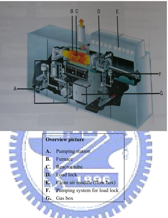
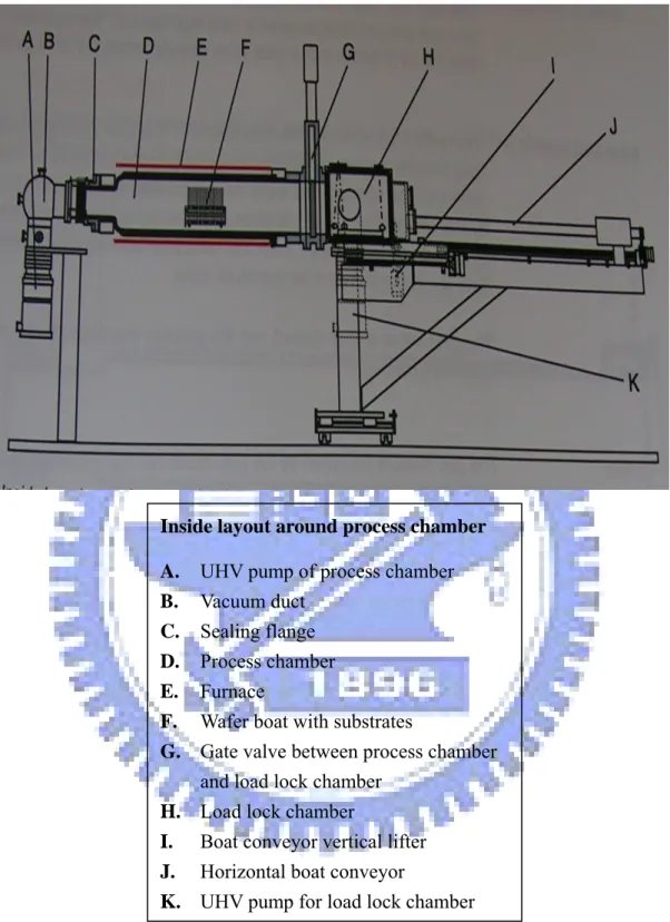
(39) substrate are required to serve as virtual substrates [22], [23]. The conventional method for achieving fully relaxed SiGe epi-layers with low threading dislocations (TDs) densities is to grow 1–2 μm thick SiGe layers, in which mismatch strain is gradually released by a modified Frank–Reed (MFR) mechanism [24], [25]. We have fabricated high-quality relaxed SiGe films using an intermediate Si or Si1–yCy layer [26, 27]. The misfit dislocations induced by the SiGe overlayers were formed or confirmed at the interface of SiGe overlayers and the intermediate Si1–yCy layers.. 2.2 UHV-CVD System Features A photograph and the configuration of the SiGe epitaxial growth system are shown in Fig. 2.1 (a) and (b). The Unaxis SIRIUS UHV-CVD tool is built as customized unit. The system differs with regard to the arrangement of the pumps, the external appearance and other details. The reactor and load lock chamber has been improved to realize ultra-clean ambient for low temperature epitaxial growth. Fig. 2.2 shows an overview picture of how the system can be laid out. The sectional view shown in Fig. 2.3 is the inside layout of the SIRIUS schematically. The process chamber (D) from a cylindrical spaces, is connected to the UHV pump (A) via the vacuum duct (B) and can be evacuated to ultra high vacuum. The duct can be disconnected from the UHV pump with a gate valve directly before the UHV pump. The reactor tube is sealed off from the atmosphere with two sealing flanges (C). The furnace (E) is laid around the process chamber. It can be electrically heated and produces an exactly specified thermal flat zone of approx. ± 0.5℃ in the process chamber with an electric controller. The process chamber is separated from the load lock chamber (H) by the gate valve (G). 22.
(40) 2.3 Epitaxy film growth 2.3.1 SiGe film The starting materials adopted were 4 inch diameter, 15–25 Ω cm, p-type (001) -oriented Si wafers. All the epitaxial films investigated in this work were grown at 600℃ in a commercially available multi-wafer UHV/CVD system (Unaxis Sirrus 400). The base pressure of the reactor is typically below 8 × 10⁻⁹ mbar. High purity SiH4, 5% GeH4 diluted in He, were used as Si, Ge and B sources, respectively. Prior to the epitaxial growth, the p-Si wafers were dipped in a 10% HF solution to maintain the H-termination on the surface of the substrate before transferred to the UHV/CVD reactor in a quartz wafer boat through a load lock which is pumped down to a base pressure of 1 × 10⁻⁶ mbar within 10 min. A 60 nm thick Si buffer layer was first grown to cover the wafer surface. Then a 700-nm-thick Si0.8Ge0.2 film (the Ge concentration linearly graded from 0 to 20% were prepared) with a 50-nmthick intermediate. Si layer was grown on the Si buffer, Finally, a 20-nm thick Si strained layer was deposited [27].. 2.3.2 SiC film Four-inch diameter, 10-25Ω cm, p-type (001)-oriented Si wafers were used as starting substrates. All structures investigated in this work were grown at 600 °C in a commercially available ultrahigh vacuum chemical vapor deposition (UHV/CVD) system. Pure SiH4, SiCH6, and 5% GeH4 diluted in He were used as precursors. Before epitaxial growth, the Si wafers were dipped in a 10% HF solution to achieve the H passivation. A 60 nm thick Si buffer layer was first grown to cover the wafer surface. A 5 nm thick intermediate Si1-yCy (y= 0.5%) layer was then grown on the Si 23.
(41) buffer. Finally, a 30 nm thick strained Si cap layer was deposited.. 2.4 CMP System Features Chemical mechanical planarization (CMP) is a process of smoothing and planed surfaces with the combination of chemical and mechanical forces, a hybrid of chemical etching and free abrasive polishing. Mechanical grinding alone causes too much surface damage, while wet etching alone cannot attain good planarization. Most chemical reactions are isotropic and etch different crystal planes with different speed. CMP involves both effects at the same time. A typical CMP tool consists of a rotating platen that is covered by a pad. The wafer is mounted upside down in a carrier on a backing film. The retaining ring keeps the wafer in the correct horizontal position. Both, the platen and the carrier are rotating. Good speed control is important. The carrier is also oscillating. For loading and unloading a robot system is installed. During loading and unloading the wafer is kept in the carrier by vacuum. During chemical mechanical polishing, pressure is applied by down force on the carrier, transferred to the carrier through the carrier axis. Beside that also gas pressure or back pressure is loaded on the wafer. The fact that high points on the wafer are subjected to higher pressures compared to lower points, hence, the removal rates there are enhanced and planarization is achieved. The slurry is supplied from above on the platen. Process relevant are the grain size and material of the abrasive component and the pH control of the slurry. We applied it to the post-CMP cleaning on SiGe buffer layer. Furthermore, the capacitor and MOSFET electrical characteristics of strained-Si re-growth on various solutions process were evaluated. Also, the CMP process was examined on the poly-SiGe TFTs.. 24.
(42) 2.5 Summary This chapter introduces the instrument used in our experiment. The epitaxy films used in chapter 3 and 4 were prepared by the UHVCVD system in ERSO/ ITRI (Division of Semiconductor Device Technology, Electronics Research and Service Organization, Industrial Technology Research Institute).. 25.
(43) References: [1] F. Schäffler, “High-mobility Si and Ge structures,” Semicond. Sci. Technol., vol. 12, pp. 1515-1549, 1997. [2] T. E. Whall and E. H. C. Parker, “SiGe heterostructures for FET applications,” J. Phys. D: Appl. Phys., vol. 31, pp. 1397-1416, 1998. [3] U. König, M. Glück and G. Höck, “Si/ SiGe field-effect transistors,” J. Vac. Sci. Technol. B, vol. 16, no. 5, pp. 2609-2614, 1998. [4] C. K. Maiti, L. K. Bera and S. Chattopadhya, “Strained-Si heterostructure field effect transistors,” Semicond. Sci. Technol., vol. 13, pp. 1225-1246, 1998. [5] D. J. Paul, “Silicon germanium heterostructures in electronics: the present and the future,” Thin Solid Films, vol. 321, no. 1-2, pp. 172-180, 1998. [7] M. V. Fischetti and S. E. Laux, “Band structure, deformation potentials, and carrier mobility in strained-Si, Ge, and SiGe alloys,” J. Appl. Phys., vol. 80, no. 4, pp. 2234-2252, 1996. [8] J. P. Dismukes, L. Ekstrom and R. J. Paff, “Lattice parameter and density in germanium silicon alloys,” J. Phys. Chem., vol. 68, pp. 3021-3027, 1964. [9] C. W. Leitz, M. T. Currie, M. L. Lee, Z. –Y. Cheng, D. A. Antoniadis and E. A. Fitzgerald, “Hole mobility enhancements in strained Si/Si1-yGey p-type metal-oxide-semiconductor field-effect transistors grown on relaxed Si1-xGex (x<y) virtual substrates,” Appl. Phys. Lett., vol. 79, no. 25, pp. 4246-4284, 2001. [10] J. W. Matthews and A. E. Blakeslee, “Defects in epitaxial multilayers,” J. Cryst. Growth, vol. 27, pp. 118-125, 1974. [11] A. G. O'Neill, P. Routley, P. K. Gurry, P. A. Clifton and A. Benedetti, “SiGe virtual substrate n-channel heterojunction MOSFETs,” Semicond. Sci. Technol., vol. 14, pp. 784-789, 1999.. 26.
(44) [12] K. Rim, J. L. Hoyt and J. F. Gibbons, “Fabrication and analysis of deep submicrometer strained-Si n-MOSFETs,” IEEE Trans. Electron Devices, vol. 47, pp. 1406-1415, July 2000. [13] S. H. Olsen, A. G. O'Neill, D. J. Norris, A G. Cullis, N. J. Woods, J. Zhang, K. Fobelets and H. A. Kemhadjian, “Strained-Si/SiGe n-channel MOSFETs: Impact of cross-hatching on device performance,” Semicond. Sci. Technol., vol. 17, pp. 655-661, 2002. [14] M. T. Currie, C. W. Leitz, T. A. Langdo, G. Taraschi and E. A. Fitzgerald, “Carrier mobilities and process stability of strained-Si n- and p-MOSFETs on SiGe virtual substrates,” J. Vac. Sci. Technol. B, Microelectron. Process. Phenom., vol. 19, no. 6, pp. 2268-2279, 2001. [15] S. H. Olsen, A. G. O'Neill, L. S. Driscoll, K. S. K. Kwa, S. Chattopadhyay, A. M. Waite, Y. T. Tang, A. G. R. Evans, D. J. Norris, A. G. Cullis, D. J. Paul and D. J. Robbins, “High performance strained-Si/SiGe n-channel MOSFETs fabricated using a novel CMOS architecture,” IEEE Trans. Electron Devices, vol. 50, pp. 1961-1969, Oct. 2003. [16] S. G. Badcock, A. G. O'Neill, and E. G. Chester, “Device and circuit performance of SiGe/Si MOSFETs,” Solid State Electron., vol. 46, no. 11, pp. 1925-1932, 2002. [17] K. Rim, J. Chu, H. Chen, K. A. Jenkins, T. Kanarsky, K. Lee, A. Mocuta, H. Zhu, R. Roy, J. Newbury, J. Ott, K. Petrarca, P. Mooney, D. Lacey, S. Koester, K. Chan, D. Boyd, M. Ieong, H. -S. Wong, “Characteristics and device design of sub-100 nm strained-Si n- and p-MOSFETs,” in Symp. VLSI Tech. Dig. , 2002, pp. 98-99. [18] E. A. Fitzgerald, M. L. Lee, C. W. Leitz and D. A. Antoniadis, “Strained-Si, SiGe, and Ge MOSFET channels,” in Proc. 3rd Int. Conf. SiGe(C) Epitaxy 27.
(45) Heterostructures (ICSi-3), 2003, pp. 167-169. [19] J. Jung, M. L. Lee, S. Yu, E. A. Fitzgerald and D. A. Antoniadis, “Implementation of both high-hole and electron mobility in strained Si/strained Si1-yGey on relaxed Si1-xGex (x<y) virtual substrate,” IEEE Electron Device Lett., vol. 24, pp. 460-462, July 2003. [20] S. E. Thompson, M. Armstrong, C. Auth, S. Cea, R. Chau, G. Glass, T. Hoffman, J. Klaus, Ma Zhiyong; B. Mcintyre, A. Murthy, B. Obradovic, L. Shifren, S. Sivakumar, S. Tyagi, T. Ghani, K. Mistry, M. Bohr, Y. El-Mansy, “A logic nanotechnology featuring strained-silicon,” IEEE Electron Device Lett., vol. 25, no. 4, pp. 191-193,. 2004.. [21] K. Rim, J. L. Hoyt and J. F. Gibbons, “Fabrication and analysis of deep submicron strained-Si n-MOSFET's,” IEEE Trans. Electron Devices, vol. 47, no. 7, pp. 1406-1415, 2000. [22] M. H. Lee, P. S. Chen, W. -C. Hua, C. -Y. Yu, Y. T. Tseng, S. Maikap, Y. M. Hsua, C. W. Liu, S. C. Lu, W. -Y. Hsieh, M. -J. Tsai, “Comprehensive low-frequency and RF noise characteristics in strained-Si NMOSFETs,” in IEDM Tech. Dig., 2003, pp. 3.6.1-3.6.4. [23] M. L. Lee, E. A. Fitzgerald, M. T. Bulsara, M. T. Currie and A. Lochtefeld, “Strained. Si,. SiGe,. and. Ge. channels. for. high-mobility. metal-oxide-semiconductor field-effect transistors,” J. Appl. Phys., vol. 97, pp. 011101-011127, 2005. [24] P. M. Mooney, “Strain relaxation and dislocations in SiGe/ Si structures,” Materials Science and Engineering, vol. 17, no. 3, pp. 105-146, 1996. [25] S. Gupta, M. L. Lee and E. A. Fitzgerald, “Improved hole mobilities and thermal stability in a strained-Si/strained-Si1–yGey/strained-Si heterostructure grown on a relaxed Si1–xGex buffer,” Appl. Phys. Lett., vol. 86, pp. 192104-6, 2005. 28.
(46) [26] S. W. Lee, P. S. Chen, M. –J. Tsai, C. T. Chia, C. W. Liu and L. J. Chen, “The growth of high-quality SiGe films with an intermediate Si layer,” Thin Solid Films, vol. 447-448, pp. 302-305, 2004. [27] S. W. Lee, Y. L. Chueh, L. J. Chen, L. J. Chou, P. S. Chen, M. H. Lee, M. -J. Tsai and C. W. Liu, “Growth of strained Si on high-quality relaxed Si1-xGex with an intermediate Si1-yCy layer,” J. Vac. Sci. Technol., vol. 23, no. 4, pp. 1141-1145, 2005.. 29.
(47) (a). (b) Fig. 2.1 Epitaxial films growth system SIRIUS (a) facade of the system and (b) process chamber.. 30.
(48) Overview picture A. B. C. D. E. F. G.. Pumping station Furnace Reactor tube Load lock Clean air module (flow box) Pumping system for load lock Gas box. Fig. 2.2 Configurations of vertical SiGe epitaxial growth system.. 31.
(49) Inside layout around process chamber A. B. C. D. E. F. G.. UHV pump of process chamber Vacuum duct Sealing flange Process chamber Furnace Wafer boat with substrates Gate valve between process chamber and load lock chamber. H. I. J. K.. Load lock chamber Boat conveyor vertical lifter Horizontal boat conveyor UHV pump for load lock chamber. Fig. 2.3 Configurations of film growth system inside layout around process chamber.. 32.
(50) Chapter 3 The CMP Process and Cleaning Solution for Planarization of Strain-Relaxed SiGe Virtual Substrates in MOSFET Application 3.1 Introduction Strained silicon on relaxed silicon-germanium (SiGe) substrates is a promising candidate for transistor performance enhancement [1]. Strain splits the degeneracy in the conduction and valence bands of Si, enhances the transport properties of electrons and holes, and provides transistor speed enhancement. High quality strained-relaxed buffer layers are required for the high performance devices. But the relaxed SiGe layers tend to have the threading dislocation and rough surface. Several methods such as the graded buffer layers [2] and low temperature buffer [3] methods have been studies. The relaxation during the growth of the visual substrate results in a cross-hatch (misfit dislocations) which increases the surface roughness. The chemical mechanical polishing (CMP) process has become the mainstream of globe planarization technique in fabrication of deep submicron integrated circuit. To reduce this surface roughness, the CMP process is applied to the grown layers to reduce the surface roughness. Some previous works have been introduced it into polishing SiGe buffer layers [4]-[10]. The high crystalline quality of the re-growth layer with smooth interface makes it possible to fabricate high performance SiGe device with low surface roughness scattering. However, the wafer surface after CMP process is seriously contaminated with particles and metallic impurities form polishing slurry. In addition, the metallic impurities will induce many crystal defects in Si wafer during 33.
數據
+7
相關文件
在1980年代,非晶矽是唯一商業化的薄膜型太 陽能電池材料。非晶矽的優點在於對於可見光
◦ 金屬介電層 (inter-metal dielectric, IMD) 是介於兩 個金屬層中間,就像兩個導電的金屬或是兩條鄰 近的金屬線之間的絕緣薄膜,並以階梯覆蓋 (step
雙極性接面電晶體(bipolar junction transistor, BJT) 場效電晶體(field effect transistor, FET).
(Another example of close harmony is the four-bar unaccompanied vocal introduction to “Paperback Writer”, a somewhat later Beatles song.) Overall, Lennon’s and McCartney’s
n Logical channel number and media information (RTP payload type). n Far endpoint responds with Open Logical
―Low-Temperature Polycrystalline Silicon Thin Film Transistor Nonvolatile Memory Using Ni Nanocrystals as Charge-Trapping Centers Fabricated by Hydrogen Plasma
Iwai , “A self-aligned emitter base NiSi electrode technology for advanced high-speed bipolar LSIs” , in IEEE Bipolar/BiCMOS Circuits and Technology Meeting , pp..
In view of that, the objective of the study was to develop an automatic optical inspection system specifically for inspecting multicrystalline silicon (mc-si) solar wafer for
