國立交通大學
電子工程學系 電子研究所
碩 士 論 文
利用溫度效應實驗分析奈米級超薄介電層
場效電晶體之遠距散射機制
Temperature-Dependent Experiment to Distinguish Remote
Scatterers in Polysilicon Ultrathin Gate Oxide MOSFETs
研究生: 光心君 Shin-Jiun Kuang
指導教授: 陳明哲 博士 Prof. Ming-Jer Chen
利用溫度效應實驗分析奈米級超薄介電層
場效電晶體之遠距散射機制
Temperature-Dependent Experiment to Distinguish Remote
Scatterers in Polysilicon Ultrathin Gate Oxide MOSFETs
研究生: 光心君 Shin-Jiun Kuang
指導教授: 陳明哲 博士 Prof. Ming-Jer Chen
國立交通大學
電子工程學系 電子研究所
碩士論文
A Thesis
Submitted to Department of Electronics Engineering & Institute of Electronics
College of Electrical and Computer Engineering National Chiao Tung University
in Partial Fulfillment of the Requirements for the Degree of
Master of Science in
Electronics Engineering August 2011
Hsinchu, Taiwan, Republic of China
I
利用溫度效應實驗分析奈米級超薄介電層
場效電晶體之遠距散射機制
研究生: 光心君 指導教授: 陳明哲 博士
國立交通大學
電子工程學系 電子研究所碩士班
摘要
由近年研究可得知,元件尺寸縮減時電子遷移率會伴隨遞減,這也指出了有 額外的碰撞機制存在,並且此機制會對下一世代的元件造成很大的影響。因此本 篇論文主旨係利用實驗萃取額外遷移率之溫度係數,進而探討N型超薄介電層場 效電晶體下的遠距離散射機制。研究方法主要藉由一系列有系統的實驗與平面場 效電晶體量子模擬器的搭配,由溫度效應去探討近年倍受爭議之遠距離庫倫散射 的來源,並分辨造成遷移率大幅下降的主要碰撞機制為表面電漿子或遠距離聲子 散射。而研究結果主要有以下兩點:(1). 即使改變表面粗糙度係數,其實驗萃取 額外遷移率得到的溫度係數皆為負值,這說明了遠距離庫倫散射的主要來源是多 晶矽空乏區中的表面電漿子。(2). 由近年的發表文獻可得知,表面電漿子之溫度 係數約為-1.0,遠距離聲子散射的係數為-2.2 左右。而在此實驗萃取額外遷移率 得到的溫度係數皆落於-1.0 附近,故我們認為表面電漿子是造成遷移率大幅下降 的主要碰撞機制。II
Temperature-Dependent Experiment to Distinguish Remote
Scatterers in Polysilicon Ultrathin Gate Oxide MOSFETs
Student: Shin-Jiun Kuang Advisor: Dr. Ming-Jer Chen
Department of Electronics Engineering and Institute of Electronics
National Chiao Tung University
Abstract
Electron mobility degradation is currently frequently encountered in highly scaled devices. This means that additional scattering mechanisms exist and will become profoundly important in next generation of devices. The aim of this work is to experimentally distinguish these remote scatterers particularly concerning the controversial arguments over remote Coulomb scatterers (RCS). To clarify whether Coulomb drag or surface optical (SO) phonons mode is responsible for the degraded electron mobility in n+-polysilicon ultrathin gate oxide nMOSFETs, we apply a novel temperature-dependent experimental method to obtain corresponding mobility component in high effective field regions. The results are remarkable: (i) in a considerable range of surface roughness amplitudes (Δ), the temperature coefficient exhibits a negative value, confirming interface plasmons in poly depletion region to be dominant remote Coulomb scatterers; and (ii) a new criterion is created with which one can experimentally distinguish interface plasmons from SO phonons: if a power-law temperature exponent is close to -1.0, additional scattering with interface plasmons dominates, while for scattering with SO phonons, lies around -2.2. In this work, we obtained whose value remains around -1.0. Hence we reasonably argue that Coulomb drag due to interface plasmons is responsible.
III
Acknowledgements
能進 309A 實驗室真的是件很幸福的事情。 很感謝陳明哲老師在碩班兩年中不僅開拓了我研究的視野,更是以身教方式 讓我學習到對研究的熱情與態度;最重要的是老師總是關心著每個學生,並給了 我們一對自由的翅膀在研究的藍天中恣意翱翔。謝謝博士班的李建志、許智育、 李韋漢和張立鳴學長,在你們的細心指導與包容下,才能讓實驗室總是充滿著笑 聲與歡樂的氣氛。沒有老師與你們,真的就不會有現在的自己。也很謝謝有同屆 的張洛豪、彭霖祥與林煜翔的陪伴,讓我總能在遇到問題時回頭就發現我不是一 個人在面對。我有一群好貼心的學弟妹們,謝謝你們總是幫我打氣並且在研究中 給予大力的協助。另外我要感謝中興電機系的張書通老師與研究室學長姐們,謝 謝老師從大學一直以來的關心跟幫忙,才能讓我到現在仍舊覺得研究是件很快樂 的事情。最後我要謝謝最愛的家人、杜立博與親愛的好朋友們,你們一直都是我 最重要的後盾與城牆,讓我隨時都能躲回你們的懷抱中獲得慰藉。 我是個幸運的人,所以能進到陳明哲老師的實驗室;我也是個幸福的人,才 能擁有不只是 Lab 夥伴關係的真感情。能遇到一群相知相惜一起做研究玩樂的朋 友,真的是件很快樂灑花的事情!謝謝你們! 2011 年 8 月 光心君IV
Contents
Chinese Abstract……….….………I English Abstract……….….………II Acknowledgements ... III Contents ... IV Figure Captions ... VI Table Captions ... X Chapter 1 Introduction... 1Chapter 2 Physical Theory and Electron Mobility Model ... 4
2.1 Physical Theory ... 4
2.1.1 Schrődinger and Poisson Self-consistent “NEP” in n-MOSFETs ... 4
2.2 Electron Mobility Model ... 9
Introduction ... 9
2.2.1 Phonon Scattering Mechanism and Model ... 10
2.2.2 Surface Roughness Scattering Mechanism and Model ... 12
2.2.3 Derivation of Two-Dimensional Mobility ... 13
2.2.4 Coulomb-Limited Mobility Model due to Ionized Impurity Atoms in the Substrate Region ... 14
2.2.5 Remote Coulomb Scattering Model due to Ionized Impurity Atoms in Polygate Depletion Region ... 15
Chapter 3 Experiment Framework ... 19
3.1 The Measurement Method of the Inversion-Layer Experimentally Assessed Effective Mobility ... 19
3.2 Extraction of Source/Drain Series Resistance ... 21
Chapter 4 Analysis and Discussion ... 23
V
4.2 The Main Source of Mobility Degradation in Polysilicon Ultrathin Gate Oxide
nMOSFETs Stacks ... 25
4.3 The Validity of Matthiessen’s rule ... 27
Chapter 5 Conclusion ... 28
References ... 29
VI
Figure Captions
Figure 1.1 The framework of this work in nMOSFETs to distinguish remote
scatterers. ... 32
Figure 2.1 The energy band diagram in a poly gate/SiO2/P-substrate system. ... 33
Figure 2.2 The flowchart of Schrödinger and Poisson self-consistent process. .... 34
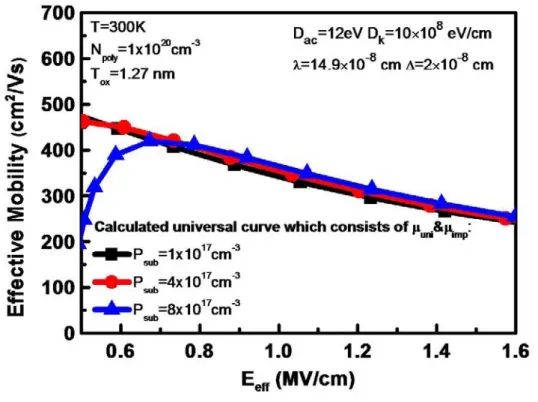
Figure 2.3 The calculated universal mobility (solid lines with symbols) versus vertical effective electric field with substrate doping concentration (Psub) as a parameter. ... 35
Figure 2.4 The simulated universal curves (solid lines with symbols) with Nsub as a parameter by different definitions of vertical effective electric field in surface roughness’s model: (a). The experimentally empirical formula. (b). The definition of vertical electric field in Eq.(2.30) [14]. ... 36
Figure 2.5 The calculated remote Coulomb-limited mobility (symbols) due to
ionized impurity atoms in polysilicon depletion region in reproducing simulated data (lines) [5], plotted versus vertical effective electric field for the three oxide thicknesses of 1, 1.5, and 2 nm. ... 37
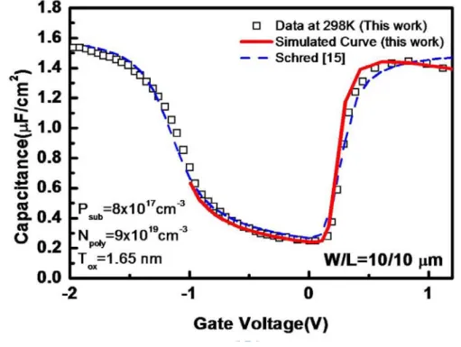
Figure 3.1 The comparison of the measured (symbol) and simulated (lines) gate capacitance versus gate voltage. In addition, the dotted lines came from the self-consistent Schrödinger and Poisson’s equations solvers [15]. 38
Figure 3.2 The schematic diagram for current flow of nMOSFETs with large gate tunneling current. Besides, IS>0 and Id<0. ... 39
Figure 3.3 Measured electron effective mobility (Solid lines with symbols) versus vertical effective electric field for (a). W/L=10/10 μm with the three temperatures of 233, 263, 298 K. (b). W/L=1/1μm with four
VII
temperatures of 292, 330, 360, and 380 K. ... 40
Figure 3.4 The simulated doping profile of nMOSFETs. Here, the blue color
represents p-type doping and red color depicts n-type one. ... 41
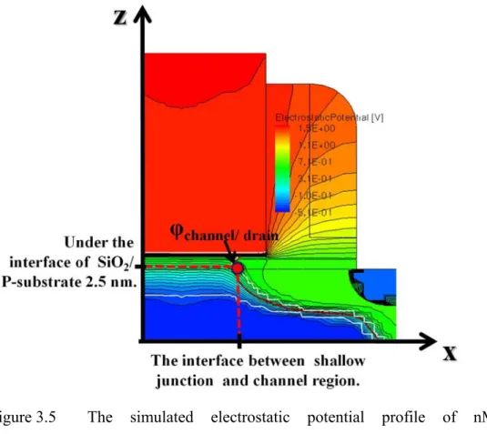
Figure 3.5 The simulated electrostatic potential profile of nMOSFETs.
/ channel drain
is the potential which locates in the surface between drain extension region and channel region. Its value is extracted below the SiO2/Si substrate interface 2.5 nm. ... 42Figure 4.1 Comparison of simulated electron universal mobility curves for two temperatures of 242K and 297K in this work (dotted lines) with the experimental one (solid lines) [17]. ... 43
Figure 4.2 Calculated effective mobility (solid lines), the simulated one (dotted lines), and the measured one (lines with symbols) for three temperatures of 233, 263, and 298 K with W/L=10/10 μm, plotted versus vertical effective electric field for (a) Δ = 2.6 Å, (b) = 2.0 Å, (c) = 1.8 Å, (d) = 1.6 Å, (e) = 1.4 Å, and (f) = 1.2 Å. ... 44
Figure 4.3 Calculated effective mobility (solid lines), the simulated one (dotted lines), and the measured one (lines with symbols) for four temperatures of 292, 330, 360, and 380 K with W/L=1/1 μm, plotted versus vertical effective electric field for (a) Δ = 1.4 Å, (b) = 1.2 Å, (c) = 1.0 Å, (d) = 0.8 Å. ... 47
Figure 4.4 The experimentally assessed additional mobility (solid lines) for three temperatures with W/L=10/10μm, plotted versus vertical effective electric field for (a) Δ = 2.0 Å, (b) = 1.8 Å, (c) = 1.6 Å, (d) = 1.4 Å, and (e) = 1.2 Å. Also shown is the calculated remote Coulomb scattering limited mobility (dotted lines) due to ionized impurity atoms
VIII
in polysilicon depletion region for three temperatures. ... 49
Figure 4.5 The experimentally assessed additional mobility (solid lines) for four temperatures with W/L=1/1μm, plotted versus vertical effective electric field for (a) Δ = 1.4 Å, (b) = 1.2 Å, (c) = 1.0 Å, and (d) = 0.8 Å. Also shown is the calculated remote Coulomb scattering limited mobility (dotted lines) due to ionized impurity atoms in polysilicon depletion region for four temperatures. ... 52
Figure 4.6 Temperature coefficients of extracting experimentally additional
mobility (solid lines) in this work, along with those of the calculated remote Coulomb scattering (RCS) limited mobility (dotted lines) due to ionized impurity atoms in polysilicon depletion region. Also represented is the possible range where the simulated temperature coefficient ... 54
Figure 4.7 Comparison of the experimentally assessed additional mobility (solid lines) near room temperature versus vertical effective electric field with the published [5] and [23] (lines with symbols). Also shown is the calculated remote Coulomb limited mobility (dotted lines) due to the ionized impurity atoms in polysilicon depletion region for three different temperatures. ... 55
Figure 4.8 Comparison of the experimentally extracted additional mobility (solid lines) near room temperature versus inversion-layer electron sheet density (Ninv), with the simulated remote Coulomb limited mobility (lines with squares) due to the interface plasmons in poly side [6], the experimentally extracted additional mobility (line with circle) from [18], and the calculated remote Coulomb scattering (RCS) limited
IX
mobility (dotted lines for three different temperatures) due to the ionized impurity atoms in polysilicon depletion region. ... 56
Figure 4.9 Calculated universal mobility curves with surface roughness amplitude (Δ) as a parameter, along with experimentally extracted mobility for temperature dependent comparison in (a). W/L=10/10 μm and (b).W/L=1/1μm. ... 57
Figure 4.10 Experimentally extracted additional mobility versus vertical effective
field with Δ = 1.2 and 1.4 Å in (a). W/L=10/10 μm for three different temperatures, and (b).W/L=1/1μm for four temperatures. The inset shows simulated inversion-layer density as a function of vertical effective field for two temperatures. ... 58
Figure 4.11 The experimental effective mobility, simulated universal mobility, and
corresponding additional one, plotted versus temperature for W/L=10/10 μm and 1/1μm at fixed inversion-layer density of 11013 cm-2 in order to make an accurate comparison with simulated interface plasmons limited mobility [6]. ... 59
Figure 4.12 Fitted temperature power-law exponent with W/L=10/10 μm (dashed
lines) and W/L=1/1 μm (solid lines) versus vertical effective field for four surface roughness amplitudes. Also shown are those from the simulated published (points) [6]. ... 60
Figure 4.13 (a) Comparison of the simulated universal mobility from two different
calculation methods between Eq. (4.3) and Eq. (4.4), plotted as a function of vertical effective electric field for three temperatures; and (b) the corresponding errors. ... 61
X
Table Captions
Table I Electron scattering and physical parameters for Si used in this work as comparison with the values in recently published. ... 62
Table II Process parameters of the devices for nMOSFETs used in this work. . 63
Table III The extracted parasitic source/ drain resistances for four temperatures with Vg=0.8, 1.0, and 1.2 V by TCAD simulator [16]. ... 64
1
Chapter 1
Introduction
It is well known that the inversion layer mobility of nMOSFETs can be limited to three primary scattering mechanisms: (1). The Coulomb impurity scattering due to the ionized impurity atoms in substrate depletion region; (2). The acoustic/optical phonon scattering in inversion channel region; and (3). The surface roughness scattering at SiO2/Si substrate interface. However, owing to the measured effective mobility that drops off in highly scaled devices, additional scattering mechanisms exist. So far, in the open literature dedicated to long-channel nMOSFETs with polysilicon ultrathin gate oxides, origins of mobility degradation remained controversial. Additional scatterers can be generalized in terms of the remote surface roughness, source/drain (S/D) plasmons, fixed oxide charge, remote Coulomb scattering, and remote phonon scattering due to surface optical (SO) phonons. First term can be removed because F. Ga´miz,et al. [1] have verified by the Monte Carlo simulation that the remote surface roughness-limited mobility increases as the inversion sheet density increases. Hence the effect on the measured effective mobility is insignificant in high vertical electric field region. Second, while channel length is shrinking into the region within Thomas-Fermi screening length (like sub-40 nm device), electron interactions occur near highly doping source/drain (S/D) and channel interface can be viewed as the dynamic screening, resulting in the excitation plasmons emission and/or absorption and then transferring the momentum to affect the current indirectly, according to the published simulation results [2]. Nevertheless, S/D plasmons can be ignored in long channel devices we used in this work. Third, the effect of fixed surface oxide charge revealed similar trends like remote surface
2 roughness mechanisms [3].
Excluding the remote scatterers mentioned above, it is essential to reconfirm the origin of main remote scatterers to distinguish between remote Coulomb scattering and SO phonons. We discussed the issue prior to remote Coulomb scattering which was thought to have two possible sources. The first source stems from ionized impurity atoms in polysilicon depletion region by Krishnan [4]. However, Yang et al.[5] examined remote Coulomb scattering because of space charge in poly side, and their simulated results have shown that it is not the primary role in mobility degradation. On the contrary, series of study by Fischetti and co-workers [6]-[8] pointed out that the free electron counterparts can give rise to interface plasmons near polysilicon and SiO2 interface which is responsible for mobility degradation when high vertical effective electric field region. This is the second source also named Coulomb drag.
Moreover, we have to further deal with the main source of degraded mobility. Although scattering by SO phonons mode is considered to be dominant in high-k dielectrics [8], its significance relative to Coulomb drag in ultrathin SiO2 gate oxide stacks was controversial in the open literature [8], [9]. From Figure 7 and Figure 8 in Ref. [8], these figures have disclosed that the decay rate of mobility with sheet density due to interface plasmons is larger than the rate by SO phonons, hence illustrating that Coulomb drag plays a major role at high inversion charge densities (Ninv>1×1013cm-2). In Ref.[9], by using inverse modeling, they extracted additional mobility and claimed that SO phonon mode is more severe in high-k dielectric than SiO2 stacks, but they didn’t take Coulomb drag in poly side into account.
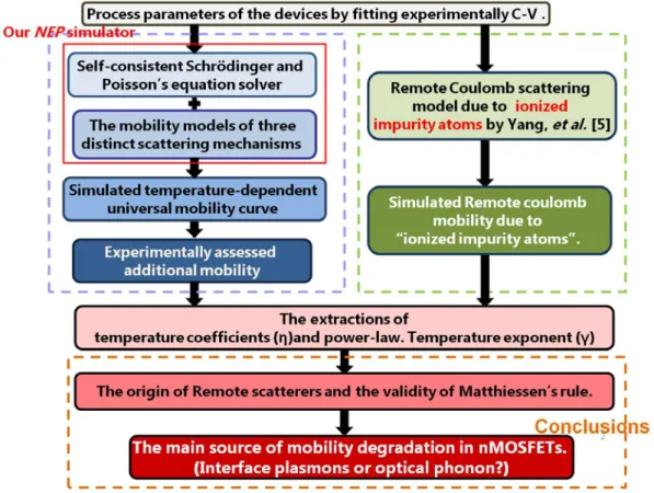
In order to clarify the discordant argument on remote scatterers, here we elaborated on a novel temperature-oriented experimental method dedicated to
3
polysilicon ultrathin gate oxide case. The flowchart of the method is shown in Figure 1.1. The proposed method in this work consists of three steps: First, we calculated the temperature-dependent effective mobility which combines the simulated universal curve and Coulomb impurity-limited mobility according to Matthiessen’s rule. Consequently, experimentally assessed additional scattering by remote scatterers would be extracted straightforwardly. For the first time, the temperature-oriented additional mobility is obtained; it can lead us to clarify the possible major role in remote scatterers. Second, we also quoted the detailed model for calculating remote coulomb scattering due to ionized impurity atoms in poly depletion region to compare with the experimental additional mobility in this work. Last but not least, a new criterion with a power-law temperature relationship of μadd Tγ is created with which one can experimentally distinguish interface plasmons from SO phonons: Based on references [6] and [7], if a power-law temperature exponent γ stays around -1.0, additional scattering with interface plasmons dominates[6]; on the contrary, while for scattering with SO phonons [7], γ is close to -2.2. These results are established on the condition of high measurement temperatures. In addition, validity of Matthiessen’s rule used in this work is addressed as well.
4
Chapter 2
Physical Theory and Electron Mobility Model
2.1 Physical Theory
2.1.1 Schrődinger and Poisson Self-consistent “NEP” in n-MOSFETs
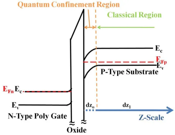
This section will introduce the fully Schrődinger and Poisson self-consistent solver in n-channel MOSFETs, particularly our established simulator “NEP” [10]. The schematic of energy band diagram is given in Figure 2.1. We separated the band diagram of silicon substrate along out-of-plane direction into two parts: one is the surface quantum confinement region (Wquantum 30 nm) and other is the bulk classical
region (Wclassical) which is defined as
1.5
classical dep quantum
W
W
W
(2.1) where Wdep is the space charge width according to abrupt depletion approximation.In the former region, the carriers are confined in this thin region with 300 mesh intervals of width dz0 0.1 nm to ensure simulation accuracy. In the latter region,
we adopt the conventional formula to handle and it is divided into 50 intervals with a width of 1
( 45)
50
dep
W
dz nm. It can significantly reduce the computational time but not losing the accuracy. Moreover, the conduction band edge at the interface is set to be zero of energy in n-MOSFETs.
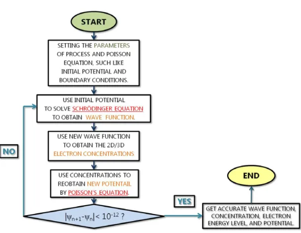
Figure 2.2 illustrates the common self-consistent steps along with the flow-chart. First, we guessed the surface band bending Vs in Poisson equation by V (z=0) =Vs and V (z=bulk) =0 for the boundary conditions. It would obtain the corresponding initial
5
potential profile V(z) and hence we can begin with the calculations of 1D Schrődinger equation along with V(z) via the formula
2 2 2m V E (2.2) According to Eq. (2.2), the Schrödinger equation can also be written as a general differential equation by the finite element method:
2 1 1 2 ( ) 2 ( ) ( ) [ ] ( ) ( ) ( ) 2 i i i i i i x x x V x x E x m x (2.3) n n n a
(2.4) where E is an eigen-value which has n values, and it is also assumed that the wave-function is confined in a small region of Wq which includes the entire inversion region completely. In general, the wave-function dividing this region into n intervals of the equal-distance x W nq / can be expanded in terms of an orthogonal basis set
n . Finally, we apply Newton’s method to solve the self-consistent Poisson and Schrődinger equations. The simulated results include n eigen-values (En) corresponding to the n wave-function (n ). The smallesteigen-value is defined as the ground state, with the others as the excited states.
. By previous paragraph mentioned, we would get the eigen-values and the wave-function. Besides, we summarize the basic formulation and the iteration that we use to perform a self-consistent solution. In the surface quantum confinement region, the three-dimensional carriers (both electrons and holes) density can be described by
, 2 3 , 2 , , ( ) ( ) ( ) ( ) i j D i j D i j i j E n z DOS E f E dE z
, ( ) 2 , 2 , ln 1+e ( ) f i j E E i DOS kT i B i j i j m g k T z
(2.5)6 , 2 3 , 2 , , ( ) ( ) (1 ( )) ( ) k j E D k j D k j k j p z DOS E f E dE z
, ( ) 2 , 2 , ln 1+e ( ) k j f E E k DOS kT k B k j k j m g k T z
(2.6) where i and k are the electron valley index and the hole valley index, respectively. j is the subband index, and gi and gk are the degeneracy of the ith valley and kth type, respectively; iDOS
m and k DOS
m are the density of states electron and hole effective mass, and Ei,j and Ek,j are the electron and hole energy levels. The corresponding wave-functions i j, and k j, are all normalized. In the bulk classical region, the carrier density is given by:
0 ( ) ( ) exp( ) B V z n z n k T (2.7) 0 ( ) ( ) exp( ) B V z p z p k T (2.8) where p0 and n0 are the carrier concentration under the thermal equilibrium. Substituting the above concentration into the 1D Poisson equation, the formula is given by 2 0 [ ( ) ( ) ( )] ( ) d si q N z n z p z d V z dz (2.9) where N zd( )
is the ionized donor density. Eventually, we can obtain a new potential
V(z) to satisfy with Eq. (2.9) and continuously iterate the procedure by Newton’s method until the potential profile V(z) is equal for successive iterations, within a tolerable error range. The two-dimensional electron density can be written as
, , 2 ln 1+e f i j E E i DOS kT i j i B m n g k T (2.10)
7
The total inversion layer charge density is shown below
, ,
inv i j i j
N
n . (2.11) and the average inversion layer thickness Zav is described as2 , , , 0 ( ) bulk i j av i j i j s n Z z z dz N
. (2.12) We demonstrated the potential calculation for the high doping poly-silicon gate situation: 2 ln( ploy sub) fb B i N N V k T n (2.13)where Vfb is the flat band voltage, Npoly and Nsub are the poly gate concentration and the substrate doping concentration, ni is the intrinsic concentration and kB is the Boltzmann’s constant.
The method to calculate poly gate voltage is similar with the potential on substrate region. Based on the electrostatics boundary conditions and abrupt depletion approximation, the following formula are given as
2
,max ,max ,max ,max
( / ) inv dep si si ox ox si poly si poly si Q Q C cm E E E E E (2. 14)
2 _ _ 1 2 ( ) D dep abrupt poly abrupt si qN x W x V x (2.15)
_ max ( ) min ( ) , 0_poly drop poly poly dep abrupt
V V x V x W x (2. 16) Therefore, using the classical concentration and Poisson equation self consistent method to converge the correct polygate voltage and extract some important results, such as the space charge density and free electron concentration in poly side by the
0( ) poly drop_
8 voltage is written as:
ox Si s ox ox t F V (2.17) where t is the oxide thickness, ox si and ox are the dielectric constant of the
silicon and oxide, respectively, and the surface electric field is given by
( 1)z (z 2) s V V F z
. Eventually, the total gate voltage can be expressed as
g s ox poly fb
V V V V V
(2.18) where V indicates the surface band bending determined by the potential profile in s the silicon substrate.
9
2.2 Electron Mobility Model
Introduction
In this section, we divided it into three parts: First, we calculated the universal electron mobility under the relaxation time approximation which uses the sub-band energy and the wave function provided by our NEP simulator. We consider only lowest four subbands in twofold valleys and two subbands in fourfold valleys to obtain corresponding mobility. Besides, we discussed the momentum relation rates caused by scattering with phonons and surface roughness which can be considered as the expression of universal curve. Second, we quoted a physically based Coulomb-limited mobility model with ionized impurities in substrate by Hauser et al. [12]. Consequently, the thick oxide effective electron mobility can be treated as the combination of the universal electron mobility and Coulomb-limited mobility according to Matthiessen’s rule. Validity of Matthiessen’s rule will be addressed in Chap.4 as well. Third, we also quoted the detailed model by Yang et al. [5] to calculate remote-Coulomb-limited mobility due to ionized impurity atoms in depletion region of n-type polysilicon gate (n-polygate) to compare with experimentally additional mobility in this work.
Figure 2.3 illustrates that the calculated universal electron mobility is insensitive to substrate concentrations or process parameters, especially when plotted as a function of high effective field (Eeff ).Eeff can be defined empirically as in the following formula 0 0 ( inv dep) eff si q N N E (2.19) where
is taken to 0.5, inversion carrier concentration(N ) and the surface inv10
concentration of the depletion charge(Ndep) are determined by NEP. Finally, all of the
scattering parameters used in this work are listed on Table I.
2.2.1 Phonon Scattering Mechanism and Model
It is well known that the pressure waves which result from the lattice vibrations would deform the crystal deformational potential, perturbing the dipole moment between atoms and giving rise to degradation of inversion layer mobility. The phonon scattering mechanisms are classified into two types, one is acoustic phonon scattering which displaces adjacent atoms in the same directions and the other is optical phonon scattering which displaces neighboring atoms in opposite directions. According to the phase of the vibration with the two different atoms in one primitive cell, acoustic phonon energy is smaller than carrier energy. The energy of the kth intervalley f-type phonon Ek(f) is 59 meV, and the energy of the kth intervalley g-type phonon Ek(g) is 63meV. Intravalley phonon scattering only considers acoustic phonons but is forbidden for optical phonons. Hence according to Takagi, et al. [13], the momentum-relaxation rate u v, ( )
ac E
from the uth subband to the vth subband is
written as:
2 1 (2 / 4) (2 / 4) 2 2 , 2 , 3 (2 / 4) , 1 1 , ( ) ( ) ac v d ac B u v u v u v ac l u v n m D k T Z z z dz Z s
(2.20)where the index of (2/4) in , (2 / 4)
u v ac
represents twofold and fourfold valleys, respectively, Dac (=12 eV) denotes the deformation potential due to acoustic phonons,
2
ac v
n (=2)and ac4 v
n (=1) are the degeneracy of the twofold valleys and fourfold valleys for intravalley scattering, respectively.
is the crystal density, s is the sound l11
velocity, Zu v, is the form factor combined with the wavefunctions of the -th subband
and the v-th subbands, is the Planck constant divided by 2π, and kB is the Boltzmann constant. The total scattering rate in uth subband is determined by summing up u v,
ac
within all the subbands, and it can be given as
, (2 / 4) (2 / 4) ( ) 1 ( ) ( ) u u u v v ac ac U E E E E
(2.21) where U x is a step function for ( ) 1(( ) U x x0), 0(x . 0)Considering the intervalley phonon scattering model, the u v, ( )
INTER E
from uth subband in twofold valleys to the vth subband in fourfold subband can be described as
2 { } 2 4 4 , ' 2 , 1 ( ) 1 1 1 1 ( ) ( ) 2 2 2 1 ( ) f f v d k k k k v u v k INTER k u v n m D f E E N U E E E E E W f E
(2.22)
, 1 ' 2( ) ' 2( ) u v u v W
z z dz (2.23) where 2 4 f vn (=4) denotes the degeneracy of the valleys about intervalley scattering,
k
E and D are the deformation energy and potential with respect to the kk th intervalley phonon, as well as m is the density-of-states effective mass of the final d4
state (fourfold valley). Besides, the signs in 1 1 2 2
k
N
indicates that “+” means phonons emission and “ - ” means phonons absorption. N signifying the k
occupation number of the kth intervalley phonon is given by
1 [exp( ) 1] k k B N E k T (2.24) Similarly, , 4'( ) u v INTER E
12 twofold subband, and ,
4( )
u v INTER E
from uth subband in fourfold valleys to the vth subband in fourfold subband, can all be written as
2 { } 4 2 2 ' , 4 , 1 ( ) 1 1 1 1 ( ) '( ) 2 2 2 1 ( ) f f v d k k k k v u v k INTER k u v n m D f E E N U E E E E E W f E
(2.25)
1 ' 2 2 , ( ) ( ) u v u v W
z z dz (2.26)
2 { } 4 4 4 ' , ' 4 , 2 { } 4 4 4 ' ' , 1 ( ) 1 1 1 1 ( ) ( ) 2 2 2 1 ( ) 1 ( ) 1 1 1 ( ) 2 2 2 1 ( ) f f v d k k k k v u v k INTER k u v g g v d k k k k v k k u v n m D f E E N U E E E E E Z f E n m D f E E N U E E E E Z f E
(2. 27) where 4 2 f v n (=2), 4 4 g v n (=1), and 4 4 f vn (=2) are the corresponding degeneracy of the intervalley phonon scattering.
2.2.2 Surface Roughness Scattering Mechanism and Model
At high effective field, the roughness scattering at the Si/SiO2 interface dominates the performance of a MOSFET device, resulting in the mobility degradation in the inversion layer. Analysis of mobility usually involves two kinds of assumptions, one is the Gaussian autocovariance function and the other is exponential autocovariance function. In this work, we prefer use of the Gaussian autocovariance function, because the calculation of surface roughness scattering rate by exponential model needs larger values of the root mean square amplitude Δ to fit experimental assessed mobility than the Gaussian model. Besides, we make an important assumption that the single subband approximation is quite accurate. Since surface roughness is anisotropic scattering, we only consider the intrasubband scattering. Under Yamakawa’s surface roughness model [14], the scattering rate for a Gaussian function is given as
13 2 2 ( ) 2 2 2 2 2 4 , 3 0 ( ) 1 ( ) (1 cos ) ( ) 2 DOS eff j ij q j i j SR m E e E U E E e d E
(2.28) Assuming the elastic collisions without energy transition, 2 2 ( ) 2 2 2 2 2 1 cos 2 , 3 0 ( ) 1 ( ) sin ( ) 2 2 j DOS eff m E E j ij j i j SR m E e E U E E e d E
(2.29) 2=2 (1 cos ) 2 q k (2.30) ( ) 2 2 2 (E-E ) = DOS j j m k (2.31) where ( ) DOS jm and Ej are the density of states effective mass and the electron subband
energy in the jth subband. Besides, the new definition of E can follow Ref. [14] effij replaces with the empirical formula Eq. (2.19) to obtain more accurate universal curves. The comparison results are depicted in Figure 2.4. The new definition of
eff ij E is written as . 0 ( ) ( ) eff ij j dV i E z z dz dz
(2.32) where i( )z and j( )z are the wavefunctions of the initial and final states of theelectrons, respectively, and E is the electron effective field from the ieffij th subband to the jth subband. When the relationship of E-K displayed a parabolic curve, the Eq. (2.17) and Eq. (2.32) would be the same definition.
2.2.3 Derivation of Two-Dimensional Mobility
The scattering rates of the twofold and fourfold valley can be expressed in terms of the phonon scattering and surface roughness scattering for ith subband with the energy (E ); hence the equations are described as [13]:
14
2 _ _
1 1 1
( ) ( ) ( )
i i i
phonon twofold SR twofold
E E E (2.33) 4 _ _ 1 1 1 ( ) ( ) ( ) i i i
phonon fourfold SR fourfold
E E E
(2.34) where i _ ( ) phonon twofold E and i _ ( ) phonon fourfold E consist of intravalley and intervalley phonon scattering for ith subband of two- and fourfold valleys. Therefore, using the average energy within the 2DEG under the relaxation time approximation, the mobility
2i and
4i for electron in ith subband of two- and fourfold valleys cab be defined as 2 2 2 ( ) ( )( ) ( )( ) i i i o E i i c E i f q E E E dE E f m E E dE E
(2.35) ' ' 4 4 ' 4 ( ) ( )( ) ( )( ) i i i o E i i c E i f q E E E dE E f m E E dE E
(2.36)Consequently, the total universal mobility
uni averaged over the subband occupation is written as ' 2 4 ' ' ( i i ) i i i i uni s N N N
(2.37)2.2.4 Coulomb-Limited Mobility Model due to Ionized Impurity
Atoms in the Substrate Region
Coulomb scattering due to ionized impurity atoms in the substrate region causes the degradation of mobility at lower effective field. Because the momentum related rates caused by Coulomb scattering was not established completely yet in NEP
15
simulator, hence we quoted a physically based Coulomb-limited mobility model by Hauser et al. [12]. It is a semi-empirical equation that various components have been modified to obtain best fitting with measured results. The corresponding mobility of Coulomb scattering can be presented by
21 1.5 _ 2 2 2 1.1 10 1 ln(1 ) 1 n C impurity BH sub BH BH T N (2.38) 19 2 2 10 2 BH n inv T N z (2.39) 300 n T T K (2.40) where denotes the Brooks-Herring equation, and BH Tn indicates the normalized temperature. Besides, the inversion charge density (N ) are calculated from NEP inv simulator.
Therefore, the calculated thick oxide effective electron mobility excluding the influence on remote-scattering mechanisms can be treated as the combination of the universal electron mobility and Coulomb-limited mobility according to Matthiessen’s rule as follows:
_ _
1
1
1
thick oxide c impurity uni
(2.41)2.2.5 Remote Coulomb Scattering Model due to Ionized Impurity
Atoms in Polygate Depletion Region
In order to clarify the origin of remote Coulomb scatterers in polygate depletion region, we refer to the momentum remote Coulomb scattering rate due to ionized impurity atoms in poly side [5] for comparison with the experimentally assessed
16
additional mobility in this work. This model only considered the lowest subband in twofold valley.
The detailed descriptions for two-dimensional (2D) electron density (ni,j), total inversion layer charge density (Ninv), and the average inversion layer thickness (Zav) have been mentioned in Section.2.2.1. By using a triangular potential approximation and a variation approach, the lowest energy level (E11) and corresponding average inversion layer thickness (Z11) can be written as
2 1 2 3 3 11 0.5 1 55 11 1.96556( ) ( )( )
( ) si dep 96 inv dep 32 inv e E N N N N m (2.42) 1 2 3 11 2 1 9 ( ) 11 4 ( ) 32 si dep inv Z m e N N (2.43)
where m1(=0.916×mo) is normal electron effective mass, and the space charge for
depletion region (Ndep) is given by
2 si d sub dep N N e (2.44) where φd is the surface band bending in substrate region, and is described by
,
,
, log( )
F F bulk B inv av sub
d F bulk g B si v E E k T eN Z N E E k T e N (2.45)
EF,bulk is the bulk Fermi energy in the substrate region.
The previous results are used for the calculation of remote Coulomb scattering (RCS) due to impurity atoms in polysilicon depletion region. Thus, the corresponding RCS rate at scattering angle is given by
2 2 2 3 2 1 ( , ) ( ) c poly e m N A S z dz (2.46)
where m (=0.19×mc2 o) is electron conductivity effective mass, and A S z( , )2 contains the screening effect of inversion layer carrier on impurity atoms in
17
polysilicon depletion region. The detailed process has been solved in [5], and the result is written as ( , ) 4 Sz o r eB e A S z D (2.47)
The parameters in Eq.(2.44) are shown below
2 0 ( ) ( ) si ox av si ox D S sB s B 3 0 ( )3 b B b S 3 2 2 (8 9 3 ) av B b Sb S b 11 3 b Z 11 11 2 ( ) ( ( ) (1 ) ln(1 )) f f B B inv E E E E k T k T o si ox B e N s k T e e ( ) 0.5 inv dep poly N N z w N (2.48)
By using Eq.(2.44) – Eq.(2.46) and integrating within the polysilicon depletion region, the momentum RCS rate due to ionized impurity is written as
2 0 1 1 cos( ) ( ) RCS d
(2.49) Hence the remote Coulomb-limited mobility due to doping impurity in poly side can be described as 0 11 0 2 0 0 ( ) ( ) E ( ) RCS RCS c f E E g E dE e m f g E dE
(2.50) where 2 2 11 2 ( ) 2 k E E m is total energy in the lowest subband, 2 2 2m
( ) (= )
g E
18
is Fermi-Dirac distribution function. Eventually, the resulting remote Coulomb mobility due to ionized impurity atoms in poly side with oxide thickness as a parameter is presented in Figure 2.5. Agreements are achieved (see Fig. 8 in [5]).
19
Chapter 3
Experiment Framework
N-channel devices under test were fabricated in a conventional 90-nm manufacturing technology with different channel width (W) and length (L): W/L=10/10 μm for Tox=1.65nm and W/L=1/1 μm for Tox=1.27 nm. Their SiO2 thin films were grown thermally, followed by NO annealing. Experimental C-V characteristics for W/L=10/10μm as depicted in Figure 3.1 were fitted well using a fully Schrödinger and Poisson self-consistent solver in our simulator (NEP) and by Schred [15]. NEP was employed in fitting the C-V data, and the resulting process parameters of the devices are given in Table II. In addition, the same parameter values are also extracted by the available self-consistent Schrődinger and Poisson’s equations solver Schred [15].
3.1 The Measurement Method of the Inversion-Layer
Experimentally Assessed Effective Mobility
In measurement method, the conventional inversion-layer mobility is usually extracted as ( ) ( ) ( ) d g g d inv g I V L I V W V eN V (3.1) ( ) ( ) d g d g d I V G V V (3.2)
where Gd is drain conductance. When Ig is small sufficiently, Gd can be presented by
ch d
I
20
current (Is). However, while gate oxides are thin enough to encounter direct tunneling current, high gate leakage current would affect the accurate determination of drain conductance (Gd ), hence the Gd is difficult to define simply by s
d I V or d d I V .
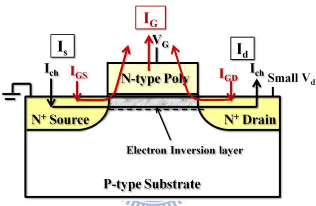
By following the experimental work by Takagi, et al. [18], we can know that while gate oxide thicknesses are quite thin, the drastically increased gate current (Ig) affects source current (Is) and drain current (Id) with the resulting opposite signs. The schematic diagram of current flow in MOSFETs with high gate leakage current is shown in Figure 3.2 where Is and Idcan be written as
s ch GS
I
I
I
(3.3)d ch GD
I
I
I
(3.4) where IGS and IGD are the current from the source to the gate and the current from the drain to gate, besides Is<0 and Id>0. Figure 3.2 illustrated that Is is larger than the current from the source into the channel (Ich) due to the current flows from source to gate(IGS), but Id is smaller than the current from channel to gate (Ich) because the current tunnels from drain into gate (IGD). When Vd is sufficiently small, the IGS must be the same as the IGD , hence the channel current can be defined as2
d s
ch
I I
I .Therefore, inversion layer (channel) mobility is measured by ( ( ) ( )) 1 ( ) 2 ( ) s g d g g d inv g I V I V L V W V EN V (3.5)
Considering the difference between Lmask and Leff, as well as the issue about the parasitic source/ drain resistance (Rsd), Eq. (3.5) could be defined more accurate by
' '
(
)
1
(
)
mask eff d s invL
L
R
eWN
(3.6)21 ' ' ' ' ' '
2
d s ds d s sd d s d sV
V
R
R
I
I
I
(3.7)where Lmask is the design length on the polysilicon etch mask andLmask Lgate . The
L
is the length of the overlap region between gate and diffusion extensions. The
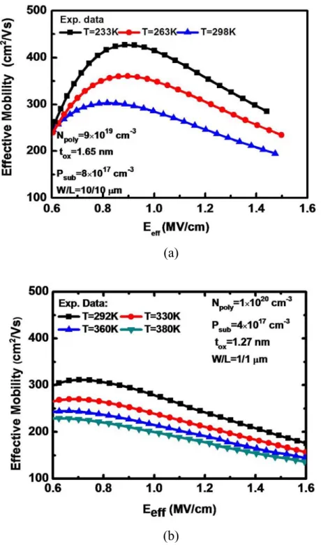
measured effective mobility values (μeff) are demonstrated in Figure 3.3 versus vertical effective field Eeff for two different gate oxide thicknesses.
3.2 Extraction of Source/Drain Series Resistance
Although the parasitic resistance in this research could be neglected, the issue of parasitic resistance should still be mentioned in this section in order to apply for short channel issue in the future.
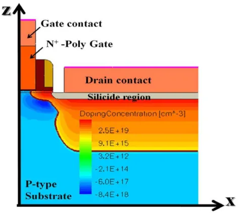
First, a state-of-the-art n-MOSFET was simulated by TCAD[16] in order to restructure the experimental one. Figure 3.4 illustrates the net doping concentration near the drain edge of n-MOSFETs (Lmask 0.065m) used in this work. The process parameters used are gate oxide thickness (Tox) =1.27 nm, n+ polysilicon doping concentration (Npoly) =1×1020cm-3, and the p-type substrate (Psub) =4×1017cm-3. The central doping concentration inside the source/ drain extension (SDE) region is higher than 1020 cm-3.The detailed doping parameter and profile were determined by fitting the measured I-V curve at T=292 K. In this situation, the method of extracting parasitic source/ drain resistance (Rsd) with Vg-dependence can be described by [19]
sd sd sd sd sd V R I I
(3.8)where Vsd 0.05V , is the potential-drop (sd
sorce channel/
channel drain/ ) between22
the interface 2.5 nm which belongs to inversion region, and I was measured by sd experiment. Eq. (3.8) regards sd
sd
V
I as total resistance (R ), and tot
sd sd I can be treated as channel resistance (R ) with Vch g-dependence, hence we can extract the series resistance (R ) by Eq. (3.8) simply. The schematic of electrostatic potential in sd channel region at Vg=1.0 V for T=292K is also shown in Figure 3.5. Further, we discuss R values under various bias conditions in three gate voltages: 0.8, 1.0, and sd
1.2 V.
The results of extracting R value are summarized in Table III. When gate sd voltage increases, the corresponding parasitic resistance decreases gradually. Regardless of temperatures used, it is found that Rsd 126 at Vg=0.8 V,
106
sd
R at Vg =1.0 V, and Rsd at V99 g =1.2V. Finally, the R values sd
obtained by using this simulation study are reasonably consistent with the extracted one ( Rsd 120 ) shown in [20]. Thus, we selected Rsd 117 as process parameter in W/L= 1/1 μm.
23
Chapter 4
Analysis and Discussion
In this section, the resulting universal mobility for a correlation length of the surface roughness (λ) of 14.9 Å and root mean square height of the surface roughness amplitude (Δ) of 2.6 Å, which are mentioned in section 2.2.3, was found to reproduce experimental data [17] well for two different temperatures (T=242K, 297K). Corresponding comparison is depicted in Figure 4.1. This confirms the validity of the temperature-dependent universal mobility simulation work. Therefore, we can use the fitting parameters as reference. Since different manufacturing procedures or oxide fabrication steps may result in different universal mobility [19], [21], we took various surface roughness amplitude (Δ) into account with the other process parameters kept fixed. With aforementioned process parameters (see Table II ) as inputs, the measured effective mobility (μeff), simulated universal curves (μuni), and the calculated universal one with no remote scatterers were plotted in Figure 4.2 for Tox=1.65nm and Figure 4.3 for Tox=1.27nm, both as a function of vertical electrical field (Eeff) with Δ as a parameter. What deserves to be mentioned is that the simulated mobility curve and calculated one would be smaller than measured data in this work when Δ = 2.6 Å in Figure 4.2(a), which is the same fitting Δ values as compared with Takagi et al.[17]. The explanation is considerable that different oxide fabrication steps correspond to different additional scattering mechanisms. While the gate oxide replaced pure oxide [17] by the SiO2 film following NO annealing as used in this work, the Δ value would decrease [21]. Therefore, Δ = 2.0 Å should be substituted for Δ = 2.6 Å as upper limit of surface roughness amplitude, and due to the improvement in the progress of manufacturing processes, Δ value should be further reduced as expected. Not only
24
did the published experiment [22] show that the extracted Δ is 1.2 Å, but also the fitting range of Δ in Fischetti [6], which will be addressed in Section4.2, yielded possible Δ range of 0.8 Å- 2Å.
4.1 The Origin of Remote Coulomb Scattering Mechanism
While comparing measured effective electron mobility (μeff), the additional scattering by remote scatterers in polysilicon region can be defined by using Matthiessen’s rule as follows:
eff _
1 1 1
thick oxide add
(4.1) the resulting additional mobilities with Δ as a parameter in W/L=10/10 μm and W/L=1/1 μm are depicted in Figure 4.4 and Figure 4.5. These figures illustrate that no matter what Δ values change, the additional scattering becomes more insignificant with decreasing temperature in universal mobility dominant region (Eeff >0.7 MV/cm). The results confirm that although we do not know the accurate Δ value in the measured samples, the simulated results all lead to one argument that the origin of remote Coulomb scattering is due to interface plasmons. The reasons are given below.
First, the conventional concept believes that a positive temperature coefficient is expected to be treated as ionized impurity atoms in polysilicon depletion region, but owing to Thomas-Fermi theory of screening effect, the higher temperature would enhance the exponential damping factor and result in the decreased screening effect, the actual trend for case of ionized impurity atoms is not so simple. In order to deal with this unknown situation, we quoted the detailed formula to calculate the remote Coulomb-limited mobility due to ionized impurity atoms in poly side as have been mentioned in Section 2.2.5. The resulting simulations are also shown in Figure 4.4 and Figure 4.5. The results point out that the calculated remote Coulomb-limited
25
mobility due to ionized impurity atoms is about two orders of magnitude larger than the experimentally assessed additional mobility.
Second, we also produced the formula of temperature-coefficient (η) to clarify the temperature-oriented trend:
(233 ) (298 ) 233 298 add K add K K K (4.2) We can find that the temperature coefficient due to ionized impurity atoms in poly side also displays large inconsistency in comparison with experimentally additional one in this work; the results are depicted in Figure 4.6.
The extra evidence suggests that remote Coulomb scattering dominates over interface plasmons as shown in Figure 4.7 and Figure 4.8. These figures showed that the published [5],[6],[18],[23] degraded mobility values at near-room temperature can be compared with experimentally assessed additional mobility in this work at T=298K. We can find that these additional mobilities from different processes [5],[6],[18],[23] are all close to our additional mobility. Besides, the remote Coulomb-limited mobility due to ionized impurity atoms in poly side is again larger than the published values [5],[6],[18],[23].
Summing up the previous contentions and the trend of additional mobility for increasing temperature which can enhance the absorption and emission of interface plasmons, we assume that interface plasmons dominate remote Coulomb scattering.
4.2 The Main Source of Mobility Degradation in Polysilicon
Ultrathin Gate Oxide nMOSFETs Stacks
In this section, we have to further clarify the main source which results in mobility degradation in polygate stacks. This concerns the degraded mobility due to
26
the surface roughness scattering mechanisms at the SiO2/Si substrate interface in high
Eeff region. To alleviate this hurdle, we used the calculated mobility curves to replicate the experimental data for different temperatures simultaneously with Δ as a parameter, the fitting results are shown in Figure 4.9. These figures all point out obviously that none of the single Δ can lead to concurrent reproduction of the measured one with different temperatures in universal dominated region; hence the remote scatterers do exist in this work.
Figure 4.10 illustrates that additional mobility exhibits an increasing trend in low Eeff region or low inversion-layer sheet density (Ninv) while decreasing gradually for higher Eeff ( Ninv >5×1012cm-2). The increasing trend of additional mobility with Eeff can be ascribed to fixed oxide charge density near SiO2/Si interface. The effect of fixed oxide charge becomes insignificant with increasing Ninv due to screening effects, and owing to decreasing screening effect with temperature, additional mobility curve at T=380K is lower than T=292K [3]. Nevertheless, in view of the applicability of Matthiessen’s rule, we only considered the high Eeff region in this work. In this situation, the effect of fixed oxide charge can be suppressed.
Figure 4.11 has shown the measured data, simulated curves, and the temperature-oriented additional mobility at Ninv =1×1013cm-2, along with the power-law relation of add T. The resulting power-law exponent γ versus Eeff is depicted in Figure 4.12. The figure reveals obviously that the γ values are all around -1.0, no matter what Eeff and Δ was adjusted.
The extra evidence is given blow. First, the simulated interface plasmons limited mobility with 1-nm gate oxide [6] in Figure 4.12 shows that the fitting γ in the same temperature region in this work is close to ours. Second, our additional mobility value is qualitatively similar with the experimentally extracted mobility [9], although we
27
cannot identify the dominated mechanisms in terms of interface plasmons in the work by Chau, et al.[9], unless we can extract the γ value to meet each other. The confirmative evidence supports that the interface plasmons are more dominant than SO phonon mode as the inversion charge density increases, as plotted in Figure 7,8 in Ref.[8]. Similar trends can be found in Figure 4.10.
Therefore, we reach the argument that Coulomb drag due to interface plasmons is the main source for degraded mobility in poly gate oxide stacks.
4.3 The Validity of Matthiessen’s rule
Finally, we want to highlight that the validity of Matthiessen’s rule in this work is adequate. Therefore, we calculated the universal mobility and the corresponding error using two different microscopic definitions:
1 1 1 ( ) ( ) ( ) i i i uni E phonon E SR E (4.3) 1 1 1 M ' ( ) ( ) ( ) i i i uni phonon SR
according to atthiessen s rule
E E E
(4.4)
The comparison results with temperatures as a parameter are shown in Figure 4.13. Obviously, although using Matthiessen’s rule would overestimate the value of universal mobility, the maximum error of universal mobility caused by using Matthiessen’s rule is below 5%. Thus, this error is insignificant as compared with the measured or simulated effective mobility difference (see Figure 4.2 and Figure 4.3). Importantly, high vertical effective electric field is involved only. Thus, the validity of Matthiessen’s rule used in this work is adequate.
28
Chapter 5
Conclusion
In this work, we have experimentally established a novel temperature-dependent method to obtain additional electron mobility due to remote scatterers and its power-law temperature exponent in ultrathin gate oxide polysilicon nMOSFETs operated at high vertical effective field.
First, in a considerable range of surface roughness amplitudes (Δ), the resulting additional mobility component for mobility degradation for the first time exhibits a negative temperature coefficient (η). We also quoted the detailed formula to calculate the remote Coulomb-limited mobility due to ionized impurity atoms in polygate depletion region. The simulated result is about two orders of magnitude larger than experimentally additional mobility in this work. The temperature coefficient (η) due to impurity atoms in poly side also exhibits a large discrepancy as compared with experimental additional one. Second, the temperature exponent (γ) extracted from experimentally additional mobility points out that the interface plasmon mode is more significant than SO phonons in this work, as supported by the existing sophisticated simulation[8].
Therefore, we reasonably confirm that Coulomb drag due to interface plasmons to be the dominant remote Coulomb scatterers and the main source of degraded mobility in ultrathin gate oxide polysilicon stacks. In addition, validity of Matthiessen’s rule used in this work has been verified .
29
References
[1]. F. Gámiz and J. B. Roldan, “Scattering of electrons in silicon inversion layers by remote surface roughness,” J. Appl. Phys., vol. 94, no. 1, pp. 392-399, July 2003.
[2]. M. V. Fischetti , S. Jin , T.-W. Tang , P. Asbeck , Y. Taur , S. E. Laux , M. Rodwell and N. Sano, "Scaling MOSFETs to 10 nm: Coulomb effects, source starvation, and virtual source model", J. Comput. Electron., vol. 8, p.60 , 2009. [3]. T. H. Ning and C. T. Sah, “Effects of inhomogeneities of surface-oxide charges
on the electron energy levels in a semiconductor surface-inversion layer,” Physical Review B, vol. 9, pp. 527-535, Jan.1974
[4]. M. S. Krishnan, Y. C. Yeo, Q. Lu, T. J. King, J. Bokor, and C. Hu, “Remote charge scattering in MOSFETs with ultra-thin gate dielectrics,” in IEDM Tech. Dig., 1998, pp. 571-574.
[5]. N. Yang, W. K. Henson, J. R. Hauser, and J. J. Wortman, “Estimation of the effects of remote charge scattering on electron mobility of n-MOSFET’s with ultrathin gate oxides,” IEEE Trans. Electron Devices, vol. 47, no. 2, pp. 440-447, Feb. 2000.
[6]. M. V. Fischetti, “Long-range Coulomb interactions in small Si devices Part II. Effective electron mobility in thin-oxide structures,” J. Appl.Phys., vol. 89, no. 2, pp. 1232–1250, Jan. 2001.
[7]. Z. Ren, M. V. Fischetti, E. P. Gusev, E. A. Cartier, and M. Chudzik, “Inversion channel mobility in high-k high performance MOSFETs,” in IEDM Tech. Dig., 2003, pp. 793-796.
[8]. M. V. Fischetti, D. A. Neumayer, and E. A. Cartier, “Effective electron mobility in Si inversion layers in metal-oxide-semiconductor systems with a
30
high-k insulator: The role of remote phonon scattering," J. Appl. Phys., vol. 90, no. 9, pp. 4587-4608, Nov. 2001.
[9]. R. Chau, S. Datta, M. Doczy, B. Doyle, J. Kavalieros, and M. Metz, “High-k/metal-gate stack and its MOSFET characteristics,” IEEE Electron Device Letters, vol. 25, no. 6, pp. 408-410, June 2004
[10]. K. H. Cheng, A Fast Quantum Simulator for the Two-Dimensional Inversion Layers,
Master Thesis, National Chiao-Tung University, Sept. 2010.
[11]. D. K. Ferry, Semiconductors (Macmillan, New York, 1991)
[12]. J. R. Hauser, “Extraction of experimental mobility data for MOS devices,” IEEE Trans. Electron Devices, vol. 43, no. 11, pp. 1981-1988, Nov. 1996.
[13]. S. Takagi, J. L. Hoyt, J. J. Welser, and J. F. Gibbons, “Comparative study of phonon-limited mobility of two-dimensional electrons in strained and unstrained Si metal-oxide-semiconductor field-effect transistors,” J. Appl. Phys., vol. 80, no. 3, p. 1567, Aug. 1996.
[14]. S. Yamakawa, H. Ueno, K. Taniguchi, C. Hamaguchi, K. Miyatsuji, K. Masaki, and U. Ravaioli, “Study of interface roughness dependence of electron mobility in Si inversion layers using the Monte Carlo method,” J. Appl. Phys., vol. 79, no. 2, pp. 911–916, Jan. 1996.
[15]. Schred. [Online]. Available: http://nanohub.org/resources/schred
[16]. TCAD. http://www.synopsys.com/Tools/TCAD/Pages/default.aspx
[17]. S. Takagi, A. Toriumi, M. Iwase, and H. Tango, “On the universality of inversion layer mobility in Si MOSFETs: Part I—Effects of substrateimpurity concentration,” IEEE Trans. Electron Devices, vol. 41, no. 12,276 pp. 2357–2362, Dec. 1994.
31
mobility lowering in ultrathin gate oxide metal-oxide-semiconductor field-effect-transistors with direct tunneling current,” Jpn. J. Appl. Phys., vol. 41, pt. 1, no. 4B, pp. 2348-2352, Apr. 2002.
[19]. D.W. Lin, M. L. Cheng, S.W.Wang, C. C.Wu, and M. J. Chen, “A novel method of MOSFET series resistance extraction featuring constant mobility criteria and mobility universality,” IEEE Trans. Electron Devices, vol. 57, no. 4, pp. 890–897, Apr. 2010.
[20]. K. Romanjek, F. Andrieu, T. Ernst, G. Ghibaudo, "Improved split C-V method for effective mobility extraction in sub-0.1-μm Si MOSFETs" EDL, p.583-5, 2004.
[21]. A. Pirovano, A. L. Lacaita, G. Ghidini, and G. Tallarida, “On the correlation between surface roughness and inversion layer mobility in Si-MOSFETs,” IEEE Electron Device Lett., vol. 21, no. 1, pp. 34–36, 367, Jan. 2000.
[22]. W. J. Zhu and T. P. Ma, “Temperature dependence of channel mobility in HfO2-gated NMOSFETs,” IEEE Electron Device Letters, vol. 25, no. 2, pp. 89-91, Feb. 2004.
[23]. Q. Xiang, G. Yeap, D. Bang, M. Song, K. Ahmed E. Ibok, and M. R. Lin, “Performance and reliability of sub-100 nm MOSFETswith ultra thin direct tunneling gate oxides,” in VLSI Symp. Tech. Dig.,Jun. 1998, pp. 160–161.
32
Figure 1.1 The framework of this work in nMOSFETs to distinguish remote scatterers.
33
34
35
Figure 2.3 The calculated universal mobility (solid lines with symbols) versus vertical effective electric field with substrate doping concentration (Psub) as a parameter.
36
(a)
(b)
Figure 2.4 The simulated universal curves (solid lines with symbols) with Nsub as a parameter by different definitions of vertical effective electric field in surface roughness’s model: (a). The experimentally empirical formula. (b). The definition of vertical electric field in Eq.(2.30) [14].
![Figure 2.5 The calculated remote Coulomb-limited mobility (symbols) due to ionized impurity atoms in polysilicon depletion region in reproducing simulated data (lines) [5], plotted versus vertical effective electric field for the three oxide thicknesse](https://thumb-ap.123doks.com/thumbv2/9libinfo/8248248.171594/49.892.151.681.366.749/calculated-polysilicon-depletion-reproducing-simulated-effective-electric-thicknesse.webp)